AMAZON multi-meters discounts AMAZON oscilloscope discounts
Both the detuned and the tuned discriminators discussed in the previous section share a disadvantage-the FM signal being de modulated must be of constant amplitude when it reaches the discriminator. In addition, the discriminator stage must be preceded by several amplifier stages, in order to build up even the weakest signal enough that the audio output from the discriminator will have sufficient volume. After this elaborate amplification process, the frequency-modulated signal must also be passed through one or more limiter stages. Here, any traces of amplitude modulation caused by atmospheric or propagation conditions are removed.
Unless these conditions are met by the two previous discriminators, they will respond to amplitude as well as frequency modulation. The result will then be a distorted audio output. This statement may be clarified with the aid of an example. In the tuned-discriminator operation, the assumption was made that at some frequency above resonance, the secondary tank voltage and the directly coupled voltage (also known as the reference voltage) were exactly in phase with each other. This caused the upper-diode detector to conduct heavily, and prevented the lower diode from conducting at all. The amount of electron current flowing through the upper diode then determined the amount of instantaneous output voltage developed across the appropriate out put resistor. This amount of electron current depended of course on the strength of the tank and reference voltages.
A little reflection on the nature of these alternating voltages will reveal that both will be large when the received signal is strong, and small when it is weak. Furthermore, these changes in signal strength will be independent of the resonant tank frequency, and also of those frequencies both above and below resonance when the three voltage waveforms are exactly in or out of phase. Consequently, when a strong FM signal is received, the amount of electron current through either diode will be caused partly by the frequency deviations of the carrier (which is good) and partly by the excessively strong amplitude of the carrier (which is bad).
CIRCUIT DESCRIPTION
The ratio detector (Figs. 8-1 through 8-4) is one of the most widely used circuits for demodulating FM signals. One reason is that it responds only to frequency deviations of the signal; it re mains unaffected by any amplitude variations caused by unusual propagation phenomena. The fact that the ratio detector is able to do this without additional amplifier or limiter stages makes it possible to build FM receivers which are competitive in price and in size with conventional AM broadcast receivers.
Circuit Components
The components and their functional titles in the ratio-detector circuit include:
R1-Output resistor.
R2-AVC resistor.
C1-Final IF tank capacitor.
C2-Capacitor for coupling the reference voltage to the detector tubes.
C3-Tuned tank capacitor.
C4-Filter capacitor for V1.
CS-Filter capacitor for V2.
C6-Large capacitor for stabilizing the voltage across C4 and C5.
C7-Coupling capacitor for the audio output.
L1-Final IF tank inductor.
L2-Tuned tank inductor.
L3-Radio-frequency choke.
V1 and V2-Diode-detector tubes.
Identification of Currents
The various electron currents at work in this circuit include:
1. Final IF tank current oscillating at the intermediate frequency between L1 and C1 (solid red).
2. Current which is directly coupled from the top of the primary tank to the center tap of the secondary tank inductor (dotted red).
3. Secondary tank current which oscillates between L2 and C3 and is supported by induction between L1 and L2 (blue).
4. Current through upper diode V1 (solid green).
5. Current through lower diode V2 (dotted green).
6. Stabilizing current flowing out of C6 and down through R2 (solid green).
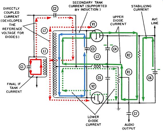
Fig. 8-1. Operation of the ratio detector-at center frequency, during
a period of normal signal strength.
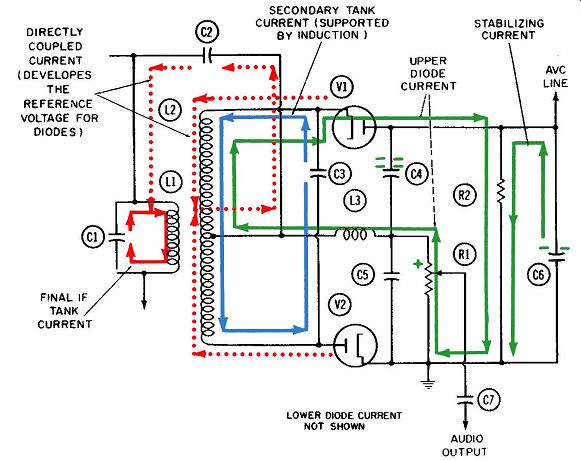
Fig. 8-2. Operation of the ratio detector-above center frequency, during
a period of normal signal strength.
CIRCUIT OPERATION
This type of circuit differs from the discriminators discussed in the previous section in three important particulars. They are:
1. The position of the lower diode, V2, is reversed, so that electron current flows in the opposite direction. This is called a series-aiding connection.
2. Both diode currents flow through output resistor R1, whereas in the discriminator circuits they flowed through separate load resistors.
3. A long time-constant combination, consisting of R2 and C6, has been added so the circuit will not respond to undesired modulations in signal amplitude.
The same waveform diagrams shown in the preceding section on the detuned discriminator also apply to this ratio detector.
The fact that the lower diode, V2, has been reversed means of course that its current flows clockwise around the lower portion of the detector circuit. The important difference between the operation of this circuit and the tuned discriminator is that diode V2 conducts during different portions of the whole cycle. How ever, the quantity of electrons conducted during any individual cycle is the same in each circuit. Because of this, the waveform diagrams of the tuned discriminator will not be repeated here.
Fig. 8-1 depicts the conditions when this circuit is operated at its center frequency. The upper-diode current (solid green) and lower-diode current (dotted green) will now flow in equal amounts. Since both diode currents are equal but flow through output resistor R1 in opposite directions, no output voltage is developed across R1.
The complete path for the electron current through upper di ode V1 is clockwise through V1, then downward through R2 to ground. From ground, the path is upward through R1 and to the left, through L3, to the center tap of L2. From here it flows up ward through the upper half of L2 and returns to the cathode.
A steady negative voltage builds up on the upper plate of capacitor C4 as a result of this current flow.
As the frequency deviates above resonance, this negative voltage on the upper plate of C4 will increase proportionately. Fig. 8-2 depicts this condition. V1 conducts more and more as the frequency increases, and V2 conducts less and less. Although Fig. 8-2 does not show any current through V2, some current usually will be flowing through it. However, the current through V1 predominates.
Fig. 8-3 depicts conditions when the ratio detector is operated at any reasonable frequency lower than the center or resonant frequency. As the frequency deviation below resonance increases, diode V2 will conduct more electron current and diode V1 will conduct progressively less. (As before, the current through V1 is not shown.) The complete path of the electron current through V2 is also clockwise, from cathode to plate and upward through the lower half of inductor L2 to the center tap. Here it flows to the right through L3, and down through R1 to the common ground connection, through which it has easy access back to the cathode.
At any frequency below resonance, more current flows through V2 than through V1. The difference between these two currents increases as the frequency deviation does. Because more current flows through V2 than through V1, more current will flow down ward through R1 than upward. This establishes the fact that the voltage at any point along R1 is negative with respect to ground.
Figs. 8-2 and 8-3 represent positive and negative half-cycles of audio-output voltage, respectively. Capacitor C6 (usually 8 or 10 microfarads) operates in conjunction with resistor R2 to form a long time-constant combination. Its purpose is to restrict the amount of current through the two diodes when the signal is excessively strong, but to encourage their flow when the signal is weak. In this respect, the combination functions somewhat like the AVC combination discussed in a previous section.
Fig. 8-4 depicts operating conditions during a signal build-up at a frequency above resonance. Now the received carrier signal is stronger. When this occurs, both of the principal currents through the two diodes will be increased proportionately. Since these currents flow in opposite directions through resistor R1, the voltage developed across R1 will depend on the difference between these two currents, As both currents are increased proportionately, so does the difference between them. Consequently, a signal build-up-one of the commonest forms of undesired amplitude modulation, along with signal fade-will change the instantaneous audio-output voltage across R1. Hence, the circuit will now respond to amplitude modulation.
This undesirable state of affairs is prevented by the voltage accumulated on the upper plate of capacitor C6. As you can see, capacitors C4 and C5 are connected in parallel with C6; there fore, the instantaneous voltages on the upper plates of C4 and C5 must always add up to the voltage on C6, even though these voltages are themselves constantly changing in step with the frequency deviations of the carrier. It is the presence of this fairly stable voltage on capacitor C6 which biases both diodes so they will conduct enough current to produce the two voltages on capacitors C4 and C5.
In summary, the voltage across capacitor C6, and simultaneously across resistor R2, will always be equal to the sum of the voltages across capacitors C4 and C5. This is inevitable, since the tops of C4 and C6 are connected together, as are the bottoms of C6 and C5. The voltages across C4 and C5 always add up to the voltage on C6, but will change individually so that their difference is always proportionate to the frequency deviation of the carrier.
When both diodes in Fig. 8-1 are conducting equal amounts of current, the voltage at the top of resistor R1 will be zero, since its bottom is connected to ground (zero) and equal currents flow in opposite directions through it. A negative voltage will exist at the top of capacitor C4. This is due to the accumulation of electrons on its upper plate as a result of the plate current through diode V1. The same negative voltage will exist from top to bottom of capacitor C6 because it is the sum of these two voltages, one of which is zero.
When operating above resonance, in Fig. 8-2 diode V1 conducts more current and delivers more electrons to the upper plate of C4.
As a result, the negative voltage across C4 increases. However, because diode V1 is conducting more electrons than V2, the top of resistor R1 must be more positive than the bottom, which is connected to ground. The reason is that more current is flowing upward through R1 than downward.
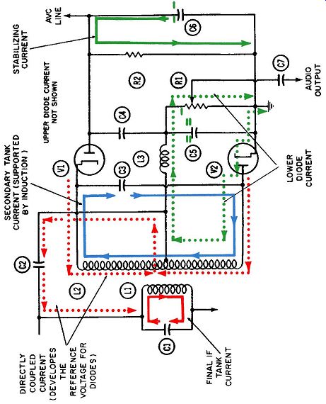
Fig. 8-3. Operation of the ratio detector-below center frequency, during
a period of normal signal strength.
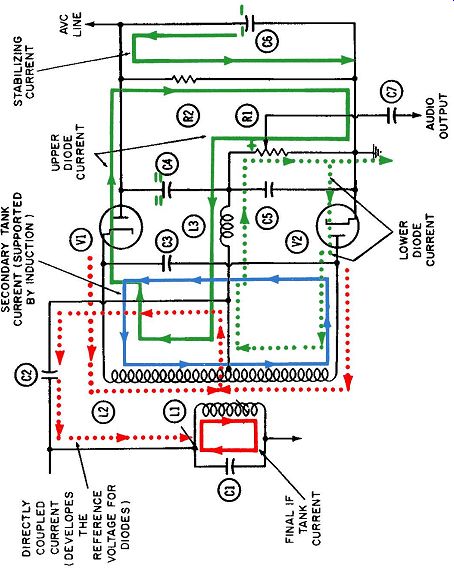
Fig. 8-4. Operation of the ratio detector-above center frequency, during
a period of signal build-up.
Because of the long time-constant of R2 and C6, the voltage across them does not change during the one-quarter of an audio cycle between Figs. 8-1 and 8-2. This voltage is represented by the electrons stored on the upper plate of C6. In Fig. 8-2 this voltage is the sum of the large negative voltage across C4 and the smaller positive voltage across C5.
When operating below resonance, diode V2 in Fig. 8-2 conducts more electrons than V1. Therefore, the top of resistor R1 must be more negative than the bottom. This negative voltage is indicated by the green minus sign at this point in the figure. The voltage across C6 and R2 is still unchanged and is now equal to the sum of the reduced negative voltage across C4 and the negative voltage which now exists across C5.