by Ed Noll
BASIC IC CLOCK AND INVERTER
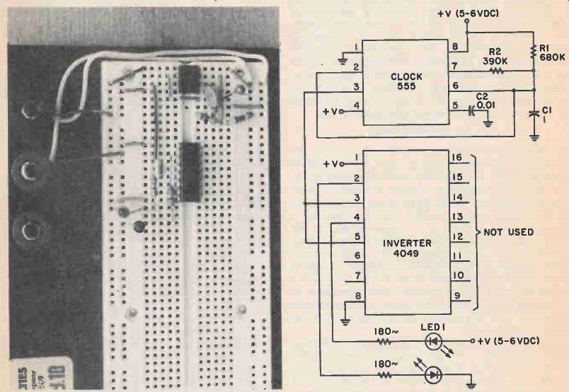
Fig. 1. Clock and inverter ICs mounted into solderless bread board. Fig.
2. Clock generator and inverter output with LED indicators.
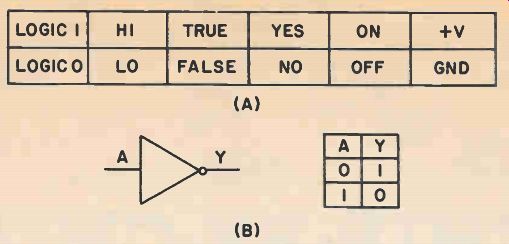
Fig. 3. Logic designations (A) and inverter and its truth table (B).
Integrated circuits (chips) are the engines of most modern electronics. Chips come in two types, linear and digital. This column will deal with the latter. The digital chip is a complex collection of electronics switches. In groups of a few or many they are the control part of computers, satellite control systems, microprocessors, cameras, watches, and most other modern devices. And, important to Electronics Handbook, and to you as readers, is the fact that chips are paramount in many of the projects presented in its pages.
In most of the articles in Electronics Handbook it is the objective of the project and the contributions of the individual chips to that objective which must be emphasized.
The objective of Chip-by-Chip is to provide details of operation on individual chip types. Not what goes on inside of each chip, but how the chip responds to input and output stimuli and conditions. The emphasis will be on what a chip can do, and how it can be made to do it. Most of this will be demonstrated with experimental circuits built on a small solderless circuit board. Important parts will be a 555 clock, one or several additional chips including the chip of interest in each column, LED's and associated parts, and finally a circuit board with its necessary hardware. Working with the parts, we will take you through a score or so of chips, at very low cost, to give you substantial growth in knowledge of chips. As an extra bonus you will gain a working knowledge of digital electronics and switching. Let's take a look at the basic clock, and an associated inverter chip.
The Versatile 555 Timer
A cheap and versatile chip is the 555 and you can expect it to be the timer chip or clock for almost all of the other chips you will learn about and experiment with in the demonstration circuits of Chip-by-Chip.
Thus it is important that in this first column you learn about clock capability. The 555 chip operates from a very low frequency up to frequencies in the megahertz, generating constant-frequency timing waveforms that swing between two voltage levels.
These are referred to as logic 0 and logic 1, as well as by several other designations mentioned later. Since we will be using LED's to display what happens with the various chip types, our 555 design will be operated at low and very low frequencies so you can see the LEDs go on and off.
All of the demo-circuits we will build on a solderless circuit board, Fig. 1. All connections are made on the board with wire jumpers. You can cut your own jumpers or, you can purchase an assortment of jumpers that fit well, and save preparation and wiring time. A third major item is a 6-volt lantern battery or a 5-volt power supply designed for digital circuit use.
The above three essential items will be used in each of the Chip-by-Chip columns.
The remainder of the parts are inexpensive. Even most of the chips will be used a number of times as back-up for the individual chip under discussion in each column. The clock is the essential test signal source. The required parts you'll need for the first two columns are given in the parts list. Most columns that follow will require only a few additional, inexpensive parts.
Three parts that will be changed in testing out the clock and in using it in later columns, are capacitor C1 and resistors R1 and R2. They are mounted at the far right in a location where they can be changed readily.
If you like you can leave slightly longer leads on these parts which will be helpful when parts of different value are substituted. Again remember to remove power when making such changes in the circuit.
Observe capacitor polarity for the wiring. Positive polarity is marked and usually is associated with longer lead. The longer lead of an LED connects to positive.
In the wiring of the 4049 inverter the top two inverters on the left side, Fig 4, are made active. The output of the clock at pin 3, Fig. 2, is connected to the inverter input at pins 3 and 5. Compare Figs. 2 and 4 to verify these connections. The output of the top left inverter is obtained from pin 2, and is applied to LED 2, at the bottom of Fig 2. When this LED turns on i indicates that the logic at the output of this inverter is 1. Of course when the output logic is 1 it means that the voltage there is +V which is applied to the anode of LED 2. The cathode is connected to ground, and the LED turns on. The 180-ohm resistor limits the LED current to a safe value.
The output wiring is different for LED 1. Notice its polarity has been changed and the anode i connected to +V. In the case of this inverter the LED turns on when the output logic at pin 4 of the second inverter is 0. Of course logic 0 represents ground.
Consequently there is a complete path for LED 1 and it will turn on when the output logic is 0.1f the output logic at pin 4 is 1 there will be no voltage drop across the LED and it will not glow. Conversely when the output logic at pin 2 of the top inverter is 0 there will also be no voltage drop across LED 2 and it will not glow. In summary, a logic 1 at output pin 2 turns on LED 2 and a logic 0 at the output of pin 4 will turn on LED 1. Consequently as the logic changes at the output of these 555 clock the two LED's will turn alternately on and off. Hence you will be able to see the clock at work. You will be able to judge the frequency of the clock as well as the relative duration of the two clock alternations, 0 and 1.
Wire you circuit board. Check and double check before applying power. When power is applied you will know the clock is operating when the two LED's turn on an off at a relatively fast rate. The° or negative alternation of the clock will be of shorter duration than the positive alternation. Thus LED 2 will turn on for a shorter interval of time than LED1. This is understandable because the logic 0 at pin 3 of the 555 clock timer is applied to pin 3 of the inverter. The inverter changes logic 0 to logic 1 at its output.
Consequently it turns on LED 2 for the duration of the logic 0 output of the clock. Conversely, for the logic 1 output of the clock, the output of the second inverter at pin 4 is 0. Under this condition LED 1 will be turned on for the longer duration of the logic 1 output of the clock.
The 555 clock is a part of each chip demonstration circuit. Also the inverter driver and its associated LEDs will be needed, as indicators to display the operating characteristics of the chip described in each issue. What you will assemble from this column are the clock and indicators for use with the columns that follow in the moths ahead.
The 555 circuit, Fig. 2, generates a repetitive pulse wave-form that switches between supply voltage and approximately 0 volts (ground) or, in the circuits arrangements used in the column, between Logic 1 and Logic 0, or Digital 1 and Digital O. These are the only two voltage states in digital circuits. But more on this later. Other ways for expressing logic are listed in Fig. 3A. A bit confusing at first, perhaps, but important to learn and remember. The inverter and LED associated with the 555 are used to indicate circuit logic.
The inverter is one of the basic digital chips. Its basic function is to change circuit logic either from 0 to 1, or from 1 to 0, as needed and as shown in Fig. 3B. The symbol for the inverter is shown and also its so called truth table. Note that when the A input is 0, the Y output is 1, and vice versa. The 4049 chip used in the demonstration circuit, Fig. 4, has six inverters housed in a 16-pin single chip as depicted in A. In digital schematics instead of displaying the entire chip the appropriate inverter symbol is used along with the pin numbers of a particular chip (as shown in Fig. 4). Example B again shows how an inverter reverses the digital logic.
There are a variety of low, and a few higher powered inverters referred to as drivers. The 4049 is one of the latter, and it supplies enough output to illuminate the LED. Hence, it is referred to as Hex (hexagonal, meaning six) Inverter Driver. The 4049 can be used to drive various other devices and you will work with it again in later columns.
---------- PARTS LIST
Integrated Circuits: Radio Shack
555 Timer
4049 Inverter
4017 Divider-Counter
6-volt lantern battery
Eveready 731 or 5 VDC power supply (well-filtered, for digital circuits)
2 LEDs Radio Shack
Capacitors: Radio Shack
0.01 uFD
0.1 uFD
1.0 uFD
10 uFD
Resistors: Radio Shack
180 ohms (two)
390 Kohms
680 Kohms
2.2 Megohms
Soiderless circuit board Radio Shack or Global (see below)
Wire jumpers (assortment)
If no Radio Shack store is near you write to Global Specialties, P.O. Box 1405 New Haven, CT 06505
--------------
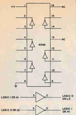
Fig 4. Inverter pin-out (4049) and inverter symbols.
Constructing and Testing the Clock
The schematic of the clock and inverter is shown in Fig. 2; the actual wiring in Fig. 1. If you have never worked with such a board before, the chips are inserted across the center groove. For each pin there then remain available four additional push-in wiring positions for that individual pin. Along both sides there are two vertical rows of continuous connections, or one for +V and the other for ground (zero VDC). Usually I use the inside row for +V and the outside for ground. Initially the chips will be mounted on the top half. In some later columns some chips will be mounted on the bottom half. In this case four additional short jumpers are needed to supply power to the bottom outside rows. This will be covered at the appropriate time. For the moment keep your circuit parts on the top half of the board.
Note the wires supplying power between plus and minus binding posts to the outside +V and ground rows. Connections are made with the battery wires by inserting banana plugs into the top of the red and black binding posts of the board. Do not apply power when making board changes. Always check the wiring twice before you apply power.
I have laid out Figs. #1 and #2 in the same way so that you can follow the schematic, and also observe how I make the same connections on the solderless circuit board. It will not be possible to do this in all cases, but it is a good idea for those who might be wiring their first solderless circuit board.
The frequency of the clock can be varied by changing the value of capacitor C1 or, by changing the values of resistors R1 and/or R2. A decline in resistance value raises frequency while an increase lowers frequency. Also an increase in capacitor value lowers frequency, and a decrease does the opposite.
Substitute a 10 mFD capacitor for C1. Now you must wait longer for the change over time between LED 1 and 2. The 'frequency in fact is reduced by a factor of approximately 10. Next substitute a 0.1 mFD capacitor. Note the high frequency output of the 555.
Finally substitute the 0.01 mFD capacitor. Now the frequency change is so fast that the LED's can no longer follow the rate of change. Nevertheless the 555 is speeding along at a fast repetition rate. Clocks in computers and other digital equipment hurry along at rates in the high megahertz range.
Restore the value of capacitor C1 to 1 mFD. Substitute a 2.2 megohm resistor for resistor R2. What has happened to the output? Of course the frequency has lowered. Also observe the LEDs are on for approximately the same length of time. The 555 clock is now generating an almost square wave. Proper resistor values and a potentiometer will let you generate a true square wave at the output of each inverter, swinging back and forth with equal durations of logic 0 and logic 1.
Join us in the next issue with your clock and inverter, and we'll go to work on the very interesting 4017 divider/counter. The components you need are already included in the parts list of this column. Have a good time!
Also see:
Adapted from: Electronics Handbook--Spring 1987