By R. D. CLEMENT and R. L. STARLIPER, Western Electric
A collection of tried and tested circuits using various types of solid-state switches that can be employed for pulse generation.
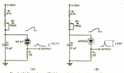
Fig. 1. (A) Neon lamp, (B) 4-layer diode relaxation oscillators.
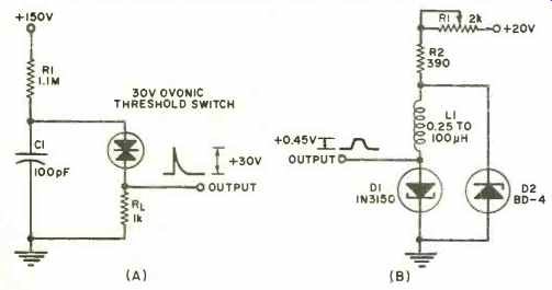
Fig. 2. (A) An ovonic switch and (B) tunnel-diode oscillators.
THE relaxation oscillator is one of the most basic types of pulse-generating circuits in use today. This kind of oscillator circuit may be designed around almost any type of nonlinear switching component. In most relaxation-oscillator circuits, the switching component is used to quickly discharge a capacitor into a low-impedance load. The particular type of switching component used determines the output pulse characteristics and frequency of operation.
During the past several years, many new switching components have appeared on the market which make a variety of relaxation oscillator circuits feasible. This article describes a number of such oscillator circuits using different components.
Neon Lamps and 4-Layer Diodes
The basic relaxation oscillator of the past consisted of a resistor, capacitor, and neon lamp connected as shown in Fig. 1A. When power =s applied to this circuit, C1 charges through R1 and R2 until the firing voltage of the neon lamp is reached. When this occurs, the gas within the lamp ionizes, causing it to switch to a low-impedance state. This causes C1 to discharge through the neon lamp until the voltage across it will no longer maintain ionization. The discharge of C1 produces an output pulse across RL each time the lamp fires. The values selected for R1, R2, and C1 control the frequency of operation of the oscillator circuit. The value of C1 must be large enough to provide adequate energy to the neon lamp to sustain oscillation. If the value of C1 is reduced below 4000 pF, the circuit will not oscillate.
Due to the ionization and deionization time of the gas within the neon lamp, the pulse characteristics of this circuit are poor. With the component values shown in Fig. 1A, the output pulse across RL has an amplitude of +0.7 volt, a width of 50 µs, and a rise time of 20 µs. With a value of 4000 pF for C1, the circuit would oscillate at a maximum frequency of 1 kHz.
The pulse characteristics of the circuit can be improved by replacing the neon lamp with a 4-layer diode, as shown in Fig. 1B. The circuit of Fig. 1B operates on the same principle as that of Fig. 1A. However, the switching time (50 ns max.) and "on" resistance (5 ohms max.) of the 4-layer diode shown improves circuit operation considerably. The output pulse measured across RL has an amplitude of +30 volts, width of 2 µs, and a rise time of 30 ns. The amplitude of this pulse may be increased by connecting several 4-layer diodes in series, thereby increasing the effective firing voltage. If three 1N3304 diodes are connected in series, the output pulse amplitude across RL will be about 90 volts.
Positive and negative pulses can be generated simultaneously by adding another load resistor in series with C1.
These pulses have the same characteristics except the amplitudes are reduced to one-half their original value. Frequencies up to 500 kHz may be obtained with the circuit of Fig. 1B if C1 is reduced to 100 pF.
Ovonic Switches and Tunnel Diodes
The circuit shown in Fig. 2A is essentially the same as that shown in Fig. 1B except the 4-layer diode has been replaced by a 30-volt ovonic threshold switch. This device will switch much faster than a 4-layer diode, producing a 30-volt output pulse with less than 8-ns rise time across RL. Since the ovonic threshold switch is a bilateral device, the polarity of the supply voltage may be changed, resulting in a negative output pulse across RL. The characteristics of the ovonic threshold switch are similar to the Motorola MPT32 3-layer diode except for switching time.
The relaxation oscillator circuit shown in Fig. 2B consists mainly of tunnel diode D1, backward diode D2, and charging inductor L1. When power is applied to this circuit, current through Dl increases according to the R1, R2, L1 time constant until its peak current is reached. When this occurs, Dl switches to its high-voltage state, producing an output pulse as shown in Fig. 2B. Backward diode D2 is used to bias Dl in its negative resistance region so as to return the circuit to its low-voltage state. The cycle is then repeated.
The operating frequency of this oscillator is controlled by the value of L1 and the output pulse width by R1. With a 0.25-µH coil for L1, the circuit operates at 10 MHz.
Crystals, UJT's and SCR's
One of the problems that exists in relaxation oscillators is frequency instability, which is due mainly to power-supply variations and component drift. If one discrete frequency is desired, the instability may be minimized by adding a crystal in the RC circuit, as shown in Fig. 3A. This circuit is a basic unijunction relaxation oscillator in which the charging capacitor has been replaced by a crystal. The operating frequency of this circuit is 99,925 ±1 Hz with a 100-kHz crystal and 999,663 ?-1 Hz with a 1-MHz crystal. The output signal at B2 of the unijunction transistor is a 2-V (p-p) distorted sine wave, as shown in the diagram.
A relaxation oscillator using an SCR as the switching component may be constructed as shown in Fig. 3B. In this circuit the R1 –C1 time constant is made small to insure that sufficient anode voltage is available to the SCR when. the gate is turned on. As the anode voltage increases, C2 charges through R2, R3, and R4 until enough energy is supplied to the gate to turn the SCR on. When the SCR conducts, C1 discharges through SCR1 and L1. The sudden discharge of C1 through L1 creates a back-e.m.f. which momentarily reverse-biases the SCR, thereby returning it to its high-impedance state. The cycle is then repeated at a frequency determined by the value of R4. The output signal taken across L1 is an 11-V (p-p), 150-µs damped sine wave as shown. With the component values given, the circuit will oscillate with a supply voltage between +5 and +35 volts.
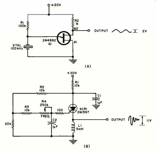
Fig. 3. (A) Crystal-UJT and (B) SCR relaxation oscillators.
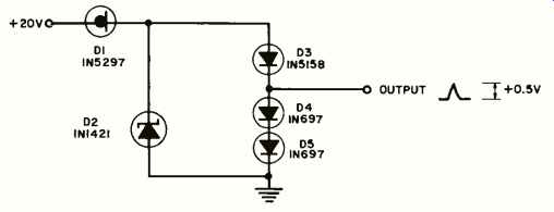
Fig. 4. A relaxation oscillator that employs all diodes.
All-Diode Oscillator
The relaxation oscillator shown in Fig. 4 is unique in that it was constructed using diodes only. When power is applied to this circuit, the junction capacitance of zener diode D2 is charged with a constant current (1 mA) from field effect diode Dl. 132 continues to charge until the forward break-over voltage of 4-layer diode D3 is reached. When this occurs, D3 fires, discharging D2 and producing a small pulse across conventional diodes D4 and D5. The operating frequency of the circuit shown is approximately 40 kHz with power-supply variations from 10 to 35 volts.
This discussion of relaxation oscillators has centered around the generation of positive and negative pulses with different amplitudes, rise times, and frequencies. Most of the oscillator circuits described can also be used to generate different types of ramp functions. For example, with the circuit of Fig. 1B, an RC ramp appears across C1 at the operating frequency of the oscillator. If resistors R1 and R2 in this circuit are replaced by a field-effect diode, as used in the circuit of Fig. 4, the ramp generated will be linear. If a field-effect diode is used in conjunction with a variable-capacitance diode in Fig. 1B, the waveform generated is an exponentially increasing function since the charging capacitor changes with voltage.
Another useful feature of the circuits shown in Figs. 1B, 2B, 3B, and 4 is that if all diodes are reversed and the polarity of the power supply is reversed, the waveforms generated will be of opposite polarity to those shown.