By JAMES E. McAllister
(Electronics World, Nov. 1971)
By using a straightedge and some simple calculations, the power dissipated during switching interval can be readily determined.
TRANSISTORS are quite often used in a saturated configuration as switches,
because a saturated transistor operated under similar circumstances will
dissipate much less power than one operating in the linear or active
configuration. This can be illustrated by the simple circuit shown in
Fig. 1A. For a device conducting a continuous current 1c, the power dissipated
by the device itself is simply the collector emitter voltage VcE (in
this case VSAT, or saturation voltage)
multiplied by the collector current 4. Since VSAT is usually quite small (several hundred millivolts), rather large amounts of current can be drawn without exceeding the power -dissipation ratings for the transistor itself. If the transistor is not saturated, the collector-emitter voltage will be larger, and less current can be conducted in a device of a given power rating.
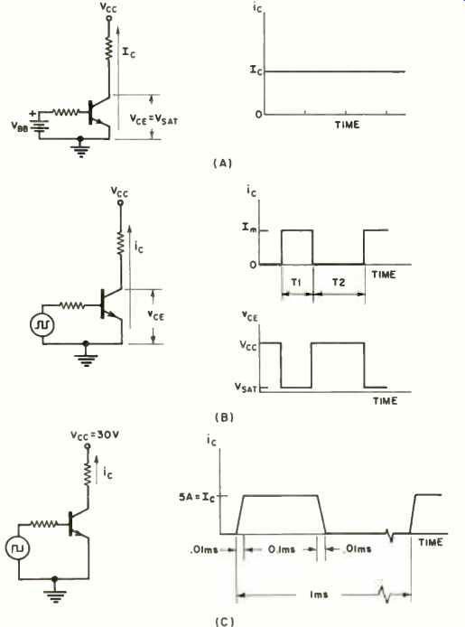
Fig. 1. Switching-transistor circuit and operating parameters.
If the transistor is not conducting continuously but is switching on and off, the problem of power dissipation is modified somewhat. Fig. 1B shows a transistor conducting current for the time T1 and not conducting for time T2.
Power is absorbed by the device only during the times (T1) when current is flowing. The average power for a complete cycle can be defined as being the maximum power multiplied by the fraction of the total time that power is actually being used.
P_AVG =(Ic X VSAT X T1)/ (T1 + T2)
The quantity T1 / (T1 + T2) is the fraction of a complete cycle of the waveform that current is being conducted. It is also called the "duty cycle" of the waveform.
The equation for average power can be applied to Fig. 1A by setting T2 equal to zero (duty cycle equal to unity). An interesting and quite useful side effect of having a small duty cycle is that large currents can be conducted for short periods of time and still have the average power dissipation remain low. For example, a device carrying 1 ampere continuously absorbs the same average power as one conducting 4 amps 1/4 of the time (duty cycle of 0.25). The current waveform shown in Fig. 1B is somewhat idealized, for it indicates that our transistor is either conducting maximum current or no current at all. In reality, the current through the device will build up from zero at a nearly constant rate. In changing from the "off" state to the "on" state or saturated condition, the transistor must pass through a period of "active" operation.
In this active region, large values of both collector current and collector-emitter voltage (and therefore large values of instantaneous power) may exist simultaneously. The power dissipated during this transition period can be minimized by performing the transition as quickly as possible.
For this reason, power lost during the switching interval of high -speed switches can often be neglected. In slow-speed circuits, however, the power lost during the switching time can contribute substantially to the total device dissipation and should be considered.
A nomogram (Fig. 2) is included to aid in estimating power during the switching interval. In order to use the nomogram, the saturation voltage for the device being considered must be known. It can be obtained from the transistor's data sheet, or can be measured as shown in Fig. 1A.
Example of Use
Problem: Estimate the transistor power dissipation in the circuit of Fig. 1C. Assume that VSAT is 1 volt.
1. First estimate the power dissipated when the transistor is fully conducting (Ic= 5 A). In this case, our duty cycle, X, will be the time of complete conduction divided by the period of the waveform.
P_AVG =ICX VSAT X lambda = 5A X 1V X 0.1 ms /1 ms = 0.5 watt.
2. Now estimate the power dissipated during one of the switching intervals. The nomogram should be used for this calculation.
A line is first drawn connecting VSAT (1 volt) and Vic (30 volts) and extended to intersect the horizontal graph axis (A). From A a line is drawn vertically to intersect the graph itself (B), and then horizontally to cross the other graph axis (C). From C, a line is projected through the value of Ic that will be used (in this case 5 amps) until the Q scale is crossed (D). A value for X is determined, and a line drawn from D through X to cross the average power axis PAVC: at E. The value of this power is the average power dissipated by the transistor during the switching control.
For this problem, X is 0.01 ms (the switching time) divided by 1 ms (period of the waveform), which gives a value of 0.01 P_AVG is approximately 270 milliwatts.
3. Next, the power dissipation during the other switching interval should be estimated. In this example, this power will also be 270 milliwatts.
4. The total average power dissipation is the sum of the individual average power dissipations.
P_AVG =0.5 +0.27 + 0.27= 1.04 watts
In this example, average power dissipated during the switching interval (0.54 watt) was more than the power used (0.5 watt) during maximum current conduction. This emphasizes the need for accurate estimation of total device power dissipation before circuit construction.
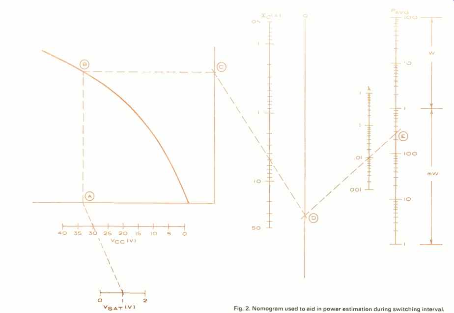
Fig. 2. Nomogram used to aid in power estimation during switching interval.
Also see: