AMAZON multi-meters discounts AMAZON oscilloscope discounts
Electronic devices have a wide range of failure modes. These can be distinguished by their development in time (sudden failure or gradual degradation), by environmental effects (e.g. corrosion, ionizing radiation) or by the electrical parameter which was exceeded (e.g. electrostatic discharge, overvoltage, overcurrent, etc.). Failures most commonly occur at the beginning and near the end of the lifetime of the parts. Burn-in procedures are used to detect early failures.
Presence of parasitic structures, irrelevant for normal operation, may become important in the context of failures; such structures can be both a source of failure and a protective device.
A sudden fail-open failure can cause multiple secondary failures, when the event is fast and the circuit contains an inductance. The suddenly interrupted current flow in combination with the inductance then causes large voltage spikes, which for very fast events may exceed 500 volts. A burned metallization on a chip may then cause secondary overvoltage damage.
Packaging-related failures
Electronic packaging, acting as the barrier between the materials of the electronic parts and the environment, is very susceptible to environmental factors. Thermal cycling may cause material fatigue due to mechanical stresses induced by thermal expansion, especially when the thermal expansion coefficients of the materials are different.
Humidity or presence of aggressive chemicals can cause corrosion of the packaging materials, leads, or cause failure of encapsulation and following damage to the part inside, leading to electrical failure. Exceeding the allowed environmental temperature, whether too high or too low, can cause overstressing of the wire bonds inside the package, tearing the connections, cracking the semiconductor dies, or causing cracks to the packaging itself. Absorption of humidity into the packaging material and subsequent heating to high temperature (e.g. during soldering) may also cause cracking. Mechanical damage could also fall here.
Majority of failure of electronics parts is typically packaging-related.
Bonding wires can be severed or shorted together during encapsulation, or touch the chip die, usually its edge. Dies can crack due to mechanical overstress or thermal shock; initial defects introduced during e.g. wafer sawing or scribing can develop to fractures later.
Lead frame may contain excessive material or burrs, causing shorts. Ions of e.g. alkali metals or halogens can be released from the packaging materials and migrate to the semiconductor dies, causing corrosion or parameter deterioration.
Glass-metal seals commonly fail by forming radial cracks. The cracks originate at the pin-glass interface and continue outwards; other failure causes are weak oxide layer on the pin-glass interface and poor formation of glass meniscus around the pin.
Moisture and other gases may be present in the package cavity, either as impurities trapped during manufacture, or from outgassing of the materials used (monomers, curing agents, etc.), or even from chemical reactions (e.g. when the packaging material gets overheated; the released reaction products, often of ionic nature, then can facilitate corrosion and cause a delayed failure). Helium is often added into the inert atmosphere of the packagings, as a tracer gas to detect leaks during testing. Carbon dioxide may result from oxidation of organic materials with residual oxygen. Hydrogen may be released from some organic materials. Moisture can be outgassed by polymers. Amine-cured epoxies may outgas ammonia.
Formation of cracks and growth of intermetallics in die attachment materials may lead to formation of voids and delamination, impairing the heat transfer from the chip die to the substrate and heatsink, and cause a thermal-related failure.
As some semiconductors, notably silicon and gallium arsenide, are transparent in infrared, infrared microscopy can be used to check the integrity of die bonding and under-die structures.
Red phosphorus, used as a charring-promoter flame retardant, facilitates silver migration when present in device packaging materials. The phosphorus particles are normally coated with aluminum hydroxide. If this coating is incomplete, the phosphorus particles oxidize to phosphorus pentoxide, which is strongly hygroscopic and reacts with moisture to phosphoric acid. Phosphoric acid acts as a corrosive electrolyte, which together with electric fields facilitates dissolution and migration of silver, forming shorts between advanced packaging pins, lead frame leads, tie bars and chip mount structures, and/or chip pads. The silver bridge may be interrupted with thermal expansion of the package; disappearance of the failure when the chip is heated with a heat gun and its reappearance after several minutes later is an indication of this problem.
Delamination and thermal expansion may move the chip die relative to the packaging, deforming and possibly shorting and/or cracking the bonding wires.
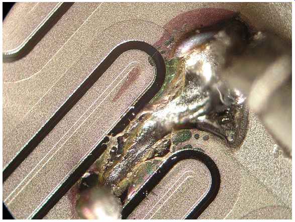
Electrical contacts
• Failures of soldered joints
• Failures of electrical contacts - mechanical faults, corrosion
• Failures of cables - fraying, breaking of the conductors, corrosion, fire damage
Soldered joints, whether on boards, cables, or inside the electronic parts themselves, can fail in many ways; by electromigration, mechanical overstress, formation of brittle intermetallic layers, or material fatigue due to excessive thermal cycling. Such failures can be apparent only at high or low joint temperatures, hindering the debugging.
Thermal expansion mismatch between the part package and the printed circuit board material stresses the part-to-board bonds. Leaded parts are able to absorb the strain by bending. Leadless chip packages rely on the properties of the solder to absorb the stresses. Thermal cycling may lead to fatigue cracking of the solder joints, especially with less plastic solders. Various approaches are used to alleviate the temperature induced strains.
Loose particles can form in the device cavity; a piece of bonding wire, a fragment of the chip die, flakes of plating, particles of die attachment material, fragments of the case, weld flash, and other materials may migrate inside the packaging cavity and cause shorts, often intermittent and sensitive to mechanical shocks.
Corrosion may cause buildup of oxides and other nonconductive products on the electrical contact surfaces. The contacts, when closed, then show unacceptably high resistance. Corrosion products may migrate and cause shorts.
Tin whiskers can form on the tin-coated metals, e.g. on the internal side of the packagings. Loose whiskers then can cause intermittent short circuits inside the packaging.
Printed circuit boards
Printed circuit boards are vulnerable to environmental influences. The traces are prone to corrosion, the vias can be insufficiently plated-through or insufficiently filled with solder.
The traces may be improperly etched, either etched-through entirely, weakened, or insufficiently etched and leaving shorts between traces. The traces may crack under mechanical loads; the thin crack then often causes unreliable circuitboard operation, dependent on the physical warping on the board. Residues of solder flux may facilitate corrosion.
Residues of other materials on the surface of the boards can cause leaks. Polar nonionic compounds can attract water molecules from the atmosphere, forming a thin layer of conductive moist coating between the traces (some antistatic agents act the same way). Ionic compounds, especially chlorides, tend to facilitate corrosion. Alkali metal ions may migrate through plastic packaging and influence the operations of the semiconductors.
Chlorinated hydrocarbon residues may hydrolyze, with release of corrosive chlorides; chlorinated solvent residues trapped in the packagings may cause problems years later.
Polar molecules may dissipate high-frequency energy, causing dielectric losses.
Above the glass transition temperature of the boards, the resin matrix softens and becomes significantly susceptible to diffusion of contaminants. As an example, polyglycols from the flux can enter the board and increase its humidity intake, with corresponding deterioration of dielectric and corrosion properties.
Multilayer substrates, using ceramics instead of fiber-reinforced polymers, suffer from mostly the same problems.
Conductive anodic filaments (CAF) may grow within the boards, along the fibers of the composite material. The metal is introduced to the vulnerable surface typically from plating the vias, then migrates in presence of ions, moisture, and electrical potential.
Drilling damage and poor glass-resin bonding promotes such failures. The formation of CAF usually begins by bonding failure between the glass fiber and the resin matrix, and a layer of adsorbed moisture then provides a channel through which ions and corrosion products migrate. In presence of chloride ions, the precipitated material is atacamite (copper chloride hydroxide); its semiconductive properties then may lead to increased leaks, deteriorated dielectric strength, and short circuits between the traces. Absorbed glycols from the flux residues aggravate the problem. The difference in thermal expansion of the fibers and the matrix also weakens the bond when the board is subjected to high temperature during soldering; the lead-free solders, which generally require higher soldering temperatures, are expected to increase the incidence of CAF. CAF incidence depends on absorbed humidity; below certain threshold it does not occur.
Delamination can occur, separating the board layers, cracking the vias and conductors and introducing pathways for corrosive contaminants and migration of conductive species.
Semiconductors
• Reliability (semiconductor)
Many failures result in generation of large amount of hot carriers in the chip structure, namely hot electrons. These are observable under an optical microscope, as they generate near-infrared photons detectable by e.g. a CCD camera. Latchups can be observed this way.
The location of the failure site, if visible, on the chip die may present clues to the nature of the overstress; whether the site is located at the place with highest current density, highest temperature, the highest electric field gradient, etc., size of the damage, secondary damage (fused leads, cracked die, reflowed die attachment...). Liquid crystal coatings can be used for localization of faults. Cholesteric liquid crystals respond to temperature, are thermochromic; these are used for visualization of locations of heat production on the chips. Nematic liquid crystals respond to voltage; these are used for visualizing current leaks through oxide defects, and for visualizing of charge states on the chip surface, allowing seeing the logical states on the individual structures and conductors.
During laser marking of plastic-encapsulated packages, the laser beam may reach and damage the chip die, if the glass spheres used as fillers in the epoxy resin packaging material line up in such way that they conduct the laser light to the chip.
Parameter-related
• GaAs MMICs:
-- Degradation of IDSS: caused by gate sinking and hydrogen effects ("hydrogen poisoning"). Most common and easiest to detect. Affected by reduction of the active channel of the transistor (gate sinking) or depletion of the donor density in the active channel (hydrogen poisoning). o Degradation in gate leakage current: occurs at accelerated life tests or high operation temperatures; suspected to be caused by surface-state effects.
-- Degradation in pinch-off voltage: common failure mode for GaAs devices, operating at high temperature. Primarily results from semiconductor-metal interactions and degradation of gate metal structures.
Can be hindered by suitable barrier metal inhibiting diffusion between gold and GaAs. Also can be caused by presence of hydrogen.
-- Increase in drain-to-source resistance: observed in devices operating at high temperature, caused by metal-semiconductor interactions. Caused by gate sinking and ohmic contact degradation.
-- Degradation in RF performance: caused by multiple factors. Surface-state density and material related effects play major roles.
In some cases, the normal presence of tolerances in the circuits can cause erratic behavior difficult to trace. For example a combination of a weak driver transistor with a higher series resistance together with the capacitance of the gate of the subsequent transistor, each within the normal "good" specifications, can significantly increase the propagation delay of the signal. Such faults can manifest only at very specific environmental conditions, high clock speeds in combination with low (but within specifications) power supply voltages, and/or specific circuit signal states. Significant variations can occur on a single die. Overstress induced damage, by e.g. creating ohmic shunts or lowering transistor output current, can potentially increase such delays, leading to erratic behavior of the circuit. As the propagation delays show significant dependence on power supply voltage, normally allowed fluctuations of power supply voltage can trigger such erratic behavior.
Vias are a common source of unwanted serial resistance on chips. Defective vias show higher resistance than they should have and therefore increase propagation delays. As their resistivity drops with increasing temperature, degradation of maximum operating frequency of the chip with decreasing temperature is an indicator of such fault.
Mousebites are regions of partially missing metallization. The conductor is still present but its width is locally decreased. Such defects usually do not show during electrical testing, but present a major reliability risk. The increased current density in the damaged region may exacerbate electromigration problems. A very significant degree of voiding is needed to create a temperature-sensitive propagation delay.
Metallization and wire bonding related
Metallization-related faults are more common and more serious cause of FET transistor degradation than bulk semiconductor material processes. Amorphous materials are promising; the lack of grain boundaries hinders interdiffusion and corrosion.
• Electromigration, caused by high current density can move atoms out of the active regions, leading to emergence of dislocations and point defects, acting as nonradiative recombination centers and producing heat instead of light.
-- Al-gate electromigration in power MOSFETs can occur with large RF signals. The current densities in the "fingers" of the gate can be sufficient to cause electromigration, leading to voids and interruptions of the gate fingers and consequent loss of control of drain current. Gold metallization is less susceptible, the issue is therefore limited to aluminum.
-- Drain contacts in power FET transistors are depleted on their end while source contacts get material deposited on them.
-- In structures using aluminum metallization over a refractory metal barrier layer, the electromigration affects primarily the aluminum layer. The underlying refractory metal is highly resistant to electromigration, so the conductor does not fail entirely; its resistance just somewhat, often erratically, increases.
The displaced aluminum can however cause shorts to neighboring structures. Addition of 0.5 - 4% of copper to the aluminum metal significantly increases resistance to electromigration; copper accumulates on the alloy grain boundaries, increasing the energy needed to dislodge the metal atoms from them.
• Metal diffusion caused by high electrical currents or voltages at elevated temperatures can move metal atoms from the electrodes into the active regions.
Some materials, notably indium tin oxide and silver, are subject to electromigration which causes leakage current and, in LEDs, nonradiative recombination along the chip edges. A barrier metal layer can be used to hinder the electromigration effects. Metal diffusion can cause changes in dimensions (and therefore parameters) of the transistor gates and other semiconductor junctions. The migration of gate layer in MESFET transistors is known as gate sinking; it reduces the dimensions of the active channel and causes change in its effective level of doping, leading to deterioration of electrical parameters.
-- Al/GaAs: Gallium arsenide in contact with aluminum, a common construction of MESFET gates, is susceptible to interdiffusion. Arsenic and especially gallium migrate into the aluminum layer, creating a zone with depleted stoichiometry, and buildup of a AlxGa1-xAs region with gradient of concentration of aluminum. AlAs crystals are formed. This manifests e.g. as an increase of the Schottky barrier height. Forward current accelerates the process in comparison with thermal-only effect.
Ti/GaAs shows similar effects. Aluminum-metalized GaAs devices two decades ago had lifetimes of thousands hours; contemporary TiPtAu metallization has lifetimes reaching millions of hours.
-- Au/GaAs: Other interface layers are used with gold; examples are Au/TiW/GaAs, Au/TiPt/GaAs, and Au/Ta/GaAs. However TiW, while best for high temperatures, has different coefficient of thermal expansion than GaAs, which leads to growth of crystal defects under the metallization and reduced carrier mobility. The industry standard structures for gates on GaAs are based on Au/Pt/Ti or Au/Pd/Ti; Ti serves as a thin interlayer to facilitate adhesion, Pt or Pd is a barrier metal hindering diffusion of Au, and Au is the thick layer conductor. Grain boundaries in the barrier metal can however facilitate increased diffusion of gold into GaAs, leading to gate sinking.
• Ohmic contact degradation. The boundary between a metallization layer and the semiconductor can degrade. In case of GaAs, a layer of gold-germanium-nickel alloy (or gold-germanium alloy) is used to achieve low contact resistance. The ohmic contact is achieved by diffusion of germanium into GaAs, forming a highly n-doped region under the metal that facilitates the connection. A thick layer of gold is then deposited over the thin layer of AuGe. Gallium atoms can migrate through the thin layer and get scavenged by the gold above, creating a defect-rich Ga-depleted zone under the contact. Gold (and oxygen) migrate in the other direction, resulting in increased resistance of the ohmic contact and depletion of effective doping level. Formation of intermetallic compounds also plays a role.
• Short circuits; mechanical stresses, high currents, and corrosive environment can lead to formation of whiskers, causing short circuits. These effects can occur both within the packaging of individual devices and on the level of circuit boards.
--- Micro-photograph of a failed TO3 power transistor due to short circuit
• Formation of intermetallic compounds, e.g. the well-known gold-aluminum intermetallics (the dreaded white and purple plagues), leading to increased contact resistance and vastly decreased mechanical reliability. This is limited to older devices.
• Formation of silicon nodules. Aluminum interconnects may be doped with silicon to saturation during deposition, to prevent alloy spikes. During thermal cycling, the silicon atoms, originally homogeneously distributed, may migrate and clump together, forming nodules. The nodules act as voids in the metallization, increasing its local resistance and lowering the device lifetime.
• Corrosion of metallization. Aluminum is highly susceptible to humidity; especially negatively biased structures can be interrupted easily. Degradation of aluminum metallization was a common cause of failures of early plastic encapsulated integrated circuits. Gold is susceptible to anodic corrosion in presence of humidity, forming voluminous conductive gold(III) hydroxide. Nickel can be extruded from metallization in presence of humidity and electric field, forming filaments along the electric field gradient that can short the electrodes.
Arsenic can be leached from GaAs in presence of moisture. To cause dry corrosion of aluminum, only trace amounts of water and ionic contaminants are required; all plastics are somewhat permeable. Phosphate ions can be leached from phosphosilicate glasses used for passivation of the chips; overcoat with oxide or oxynitride layer can be used in modern processes to create a moisture barrier on top of the phosphate glass layer, and/or a borophosphosilicate glass can be used to lower the phosphate content. Halogenides also rapidly corrode aluminum. Chlorides can be transported through the packaging from the outside.
Bromides can be liberated from brominated flame retardants present in the packaging plastics when heated above 250°C; overheating such package during storage, manufacture or use can increase the part's susceptibility to corrosion in the future.
• Sodium contamination, together with less common lithium and potassium. These ions are mobile in silicon dioxide layers even at normal temperature. (Their counterpart anions in contrast stay immobilized in the oxide structure.) The electric fields present during operation of the semiconductors cause migration of the mobile ions, leading to buildup of charged areas in the gate oxide. The NMOS gates are especially susceptible; a positive gate bias repels the cations towards the junction, depressing its threshold voltage. Even low concentrations of mobile ions can cause shifts by few millivolts, enough to cause trouble for analog circuits. The ion migration is a slow process, causing slow gradual drift of circuit parameters up to a possible failure. This effect was observed especially in early metal-gate CMOS logic circuits. Baking the affected chips at 200 °C for a few hours can temporarily reverse the effect by re-diffusing the ions through the oxide. Doping the polysilicon of the base region with phosphorus is an effective way for immobilizing the ions. Alkali ions can migrate from the outside of the package; plastics can hinder their movement but can not slow them entirely. Nitride or phosphate glass layers are used as a chip die protection against externally originated contaminants.
• Very narrow interconnection cracks can maintain functionality by electron tunneling across the crack. Cold temperatures cause contraction of the metal, widening the crack and reducing the tunneling. Devices suffering this failure can run at higher frequencies at higher temperatures; this unusual behavior is symptomatic for an interconnection crack.
• Metallization step coverage, or microcracking, is an insidious unscreenable manufacturing failure. The metallization layer at some places, where their height differs, due to geometrical constraints and deposition technique forms locally weakened sites. The metal on such steps is thinner than required, or even develops a microcrack. The increased current density then leads to other effects leading to interruption of the layer and premature failure of the device.
Semiconductor-related
• Nucleation and growth of dislocations are known mechanisms for degradation of the semiconductor junctions. This requires a presence of an existing defect in the crystal and is accelerated by heat, high current density, and emitted light. In case of LEDs, Gallium arsenide and aluminum gallium arsenide are more susceptible to this mechanism than gallium arsenide phosphide and indium phosphide.
Because of different properties of the active regions, gallium nitride and indium gallium nitride are virtually insensitive to this kind of defect.
• Accumulation of charge carriers trapped in the gate oxide of MOSFETs. This introduces permanent gate biasing, influencing the transistor's threshold voltage.
This effect may be caused by hot carriers injection, ionizing radiation (one of the total dose effects), or even nominal use; in case of EEPROM cells and related structures this is the major wear mechanism limiting the number of erase-write cycles.
• Ionizing radiation and neutron radiation have multiple effects, both transient and permanent. They can cause defects in the semiconductor, creating recombination centers and shortening the lifetime of minority carriers, degrading the performance of bipolar junction transistors; it also causes accumulation of charge carriers discussed above. More details are described in the problematics of radiation hardening.
• Migration of charge carriers from floating gates, limiting the lifetime of stored data in EEPROM and flash EPROM structures.
• Improper passivation; corrosion effects are a significant source of delayed failures. Semiconductor materials, metallic interconnects, and passivation glasses are all susceptible to corrosion. The surface of semiconductor, subjected to moisture, develops a layer of oxide; the hydrogen liberated from water then reacts with deeper layers of the material, yielding volatile hydrides.
• Stress Induced Leakage Current is an increase in the gate leakage current of a MOSFET, due to defects created in the gate oxide during electrical stressing.
• Hot carrier injection, occurring in MOSFET transistors. At high field gradients, the charge carriers (electrons in NMOS, holes in PMOS) are accelerated to high speeds. When the transistor operates at saturation with high drain-source voltage, the pinched-off region under the gate (created by the electric field) produces hot carriers near the drain end. Due to lower mobility of holes, the NMOS devices produce hot carriers at lower field gradients than PMOS; e.g. a 3 micrometer NMOS will generate hot electrons at 10 V, while a PMOS of the same size will not generate hot holes below 20 V. Some of the hot carriers, after collision with atoms in the drain region, are deflected into the gate oxide. Most return back, but some become trapped in the oxide imperfections. These then accumulate and cause a persistent gate bias, increasingly shifting the threshold voltage as more hot carriers accumulate. Like with alkali ions, the damage can be partially or fully annealed by heating the chip without power at 200-250 °C for a couple of hours.
Avalanche breakdown is also a major source of hot carriers; in case of diffused junction it usually occurs near the surface, where the dopant concentration is highest.
• Parasitic channels can form anywhere where a source-drain structure exists. The role of the gate can be played by a metallization trace above, or even by static charge built up or migrated into the overlaying insulator, protective overcoat, or passivation layer. As the migrating charge carriers are usually electrons, parasitic PMOS transistors tend to be formed. The bipolar chips are more sensitive, likely because of more stringent requirements regarding absence of mobile ionic species for CMOS and BiCMOS technologies.
• Burnt fuses, used for programming the integrated circuits, can under certain conditions reform. Polysilicon fuses may crack instead of vaporizing, which prematurely interrupts the current and leaves enough material to allow reforming the fuse later. Programming both polysilicon and metallization fuses after packaging the circuit prevents the metal from dispersing; the metal stays in the vicinity of the burnt fuse and can migrate back.
• Random access memory chips suffer from several types of failures:
-- Address fault, where the memory address decoder is faulty
-- Stuck-at fault, where a data line somewhere on the chip is shorted to H or L
-- Bridging fault, where two inputs or outputs are shorted together
-- Transition fault
-- n-cell coupling fault
-- Delay fault, where a propagation delay somewhere in the circuit is unacceptably high, causing faulty operation at high speeds
-- Retention fault, where a DRAM cell capacitor does not reliably hold charge for sufficient time
The failures are also classed as bit failures (single, double, triple, quadruple, multiple), row failures (where the entire row of bits fails), column failure (same for the memory array column), cross (where both a row and a column failure occurs), continuous block, peripheral logic, and systemic defect.
Stress-related
Most stress-related failures are electrothermal in nature. The locally increased temperature can lead to immediate failure by melting or vaporizing metallization layers, melting the semiconductor, or creating other structural changes. The diffusion and electromigration effects tend to be accelerated by high temperature, which shortens the lifetime of the device. Damages to junctions that do not lead to immediate failure manifest as altered current-voltage characteristics of the junctions.
Electrical overstress failures can be classified as thermally induced failures, electromigration related failures, and electric field related failures.
• Thermal runaway: Nonhomogenities in the substrate, causing localized loss of thermal conductivity, can cause thermal runaway where heat causes damage which causes more heat etc. Most common ones are voids caused by incomplete soldering, or by electromigration effects and Kirkendall voiding.
• Current crowding, non-homogenous distribution of the current density over the junction, formation of current filaments. This may lead to creation of localized hot spots, which poses risk of thermal runaway.
• Reverse bias: Although e.g. the LED is based on a diode junction and is nominally a rectifier, the reverse-breakdown mode for some types can occur at very low voltages and essentially any excess reverse bias causes immediate degradation, and may lead to vastly accelerated failure. 5 V is a typical, "maximum reverse bias voltage" figure for ordinary LEDs, some special types may have lower limits.
• Overcurrent can cause failures of the bonding wires. In some cases the semiconductor junctions can withstand high enough current to melt the bonding wires.
• Zener diodes in reverse bias, when severely overloaded, fail as a short circuit. A sufficiently high voltage causes an avalanche breakdown of the Zener junction; the voltage across the junction together with a significant current being forced through causes extreme localized heating; the junction and metallization melt, and an alloy of silicon and aluminum shorts the diode's terminals. This is sometimes intentionally used in semiconductors as a type of programming fuses.
• Latchups can occur when the device is subjected to an overvoltage or undervoltage pulse. The opened SCR parasitic structure then can cause an overcurrent-based permanent failure. In integrated circuits, latchups are divided by their cause to internal (transmission line reflections, ground bounces, power supply overshoots) and external (signals injected to the chip via its I/O pins from the outside). External latchups can be triggered by an electrostatic discharge.
Effects of ionizing radiation and cosmic rays are also included in external effects.
Susceptibility to latchup is tested according to the JEDEC78 test standard.
Latchup can be triggered by charge carriers injected into the chip substrate by e.g. a current flowing through an ESD protection diode, or through another latchup.
• FET transistors are sensitive to dV/dt failures; excessively fast voltage transients can cause the transistor to open.
• Bipolar transistors are more thermally sensitive than FETs; the thermal runaway phenomenons limit their operation margins at higher ambient temperatures.
Bipolar transistors are also more sensitive to degradation of die cooling mechanisms (die bond defects, part-heatsink attachment degradation).