AMAZON multi-meters discounts AMAZON oscilloscope discounts
Multipactor effect
The multipactor effect is a phenomenon in radio frequency (RF) amplifier vacuum tubes and waveguides, where, under certain conditions, secondary electron emission in resonance with an alternating electric field leads to exponential electron multiplication, possibly damaging and even destroying the RF device.
Description
The multipactor effect occurs when electrons accelerated by radio-frequency (RF) fields are self-sustained in a vacuum (or near vacuum) via an electron avalanche caused by secondary electron emission. The impact of an electron to a surface can, depending on its energy and angle, release one or more secondary electrons into the vacuum. These electrons can then be accelerated by the RF fields and impact with the same or another surface. Should the impact energies, number of electrons released and timing of the impacts be such that a sustained multiplication of the number of electrons occurs, the phenomenon can grow exponentially and may lead to operational problems of the RF system such as damage of RF components or loss/distortion of the RF signal.
Mechanism
The mechanism of multipactor depends on the orientation of an RF electric field with respect to the surface. There are two types of multipactor: two-surface multipactor on metals and single-surface multipactor on dielectrics.
Two-surface multipactor on metals
This is a multipactor effect that occurs in the gap between metallic electrodes. Often, an RF electric field is normal to the surface. A resonance between electron flight time and rf field cycle is a mechanism for multipactor development.
The existence of multipactor is dependent on the following three conditions being met: The average number of electrons released is greater than or equal to one per incident electron (this is dependent on the secondary electron yield of the surface) and the time taken by the electron to travel from the surface from which it was released to the surface it impacts with is an integer multiple of one half of the RF period and the average secondary electron yield is greater than or equal to one.
Single-surface multipactor on dielectrics This is a multipactor effect that occurs on a dielectric surface. Often, an RF electric field is parallel to the surface. The positive charge accumulated on the dielectric surface returns electrons back to the surface. A single surface multipactor event is also possible on a metallic surface in the presence of a crossed static magnetic field.
Frequency-Gap Product in Two Surface Multipactor
The conditions under which multipactor will occur in two surface multipactor can be described by a quantity called the frequency-gap product. Consider a two surface setup with the following definitions:
d, distance or gap between the surfaces
ω, angular frequency of the RF field V0, peak plate to plate RF voltage
E0, peak electric field between the surfaces, equal to V0/d.
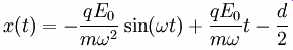
The RF voltage varies sinusoidally. Consider the time at which the voltage at electrode A passes through 0 and starts to become negative. Assuming that there is at least 1 free electron near A, that electron will begin to accelerate to the right toward electrode B. It will continue to accelerate and reach a maximum velocity ½ of a cycle later just as the voltage at electrode B begins to become negative. If the electron(s) from electrode A strike electrode B at this time and produce additional free electrons, these new free electrons will begin to accelerate toward electrode A. The process may then repeat causing multipactor. We now find the relationship between the plate spacing, RF frequency, and RF voltage that causes the strongest multipactor resonance.
Consider a point in time at which electrons have just collided with electrode A at position d/2. The electric field is at zero and is beginning to point to the left so that the newly freed electrons are accelerated toward the right. Newton's equation of motion of the free electrons is:
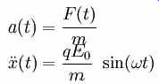
The solution to this differential equation is:
---------
where we've assumed that when the electrons initially leave the electrode they have zero velocity. We know that resonance happens if the electrons arrive at the rightmost electrode after one half of the period of the RF field, . Plugging this into our solution for x(t) we get:

Rearranging and using the frequency f instead of the angular frequency gives
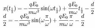
The product fd is called the frequency-gap product. Keep in mind that this equation is a criterion for greatest amount of resonance, but multipactor can still occur when this equation is not satisfied.
History
This phenomenon was first observed by the French physicist Camille Gutton, in 1924, at Nancy.
Multipactor was identified and studied in 1934 by Philo T. Farnsworth, the inventor of electronic television, who attempted to take advantage of it as an amplifier. More commonly nowadays, it has become an obstacle to be avoided for normal operation of particle accelerators, vacuum electronics, radars, satellite communication devices, and so forth. A novel form of multipactor has been proposed (Kishek, 1998), and subsequently experimentally observed, in which charging of a dielectric surface considerably changes the dynamics of the multipactor discharge.
Phosphor
--- Example of phosphorescence
----- Monochrome monitor
------ Aperture grille CRT phosphors
A phosphor, most generally, is a substance that exhibits the phenomenon of luminescence. Somewhat confusingly, this includes both phosphorescent materials, which show a slow decay in brightness (>1ms), and fluorescent materials, where the emission decay takes place over tens of nanoseconds. Phosphorescent materials are known for their use in radar screens and glow-in-the-dark toys, whereas fluorescent materials are common in CRT screens, sensors, and white LEDs.
Phosphors are transition metal compounds or rare earth compounds of various types. The most common uses of phosphors are in CRT displays and fluorescent lights. CRT phosphors were standardized beginning around World War II and designated by the letter "P" followed by a number.
Note: Phosphorus, the chemical element from the phenomenon draws its name from, emits light under certain conditions, but this is due to chemiluminescence, not phosphorescence.
Principles
A material can emit light either through incandescence, where all atoms radiate, or by luminescence, where only a small fraction of atoms, called emission centers or luminescence centers, emit light. In inorganic phosphors, these inhomogeneities in the crystal structure are created usually by addition of a trace amount of dopants, impurities called activators. (In rare cases dislocations or other crystal defects can play the role of the impurity.) The wavelength emitted by the emission center is dependent on the atom itself, and on the surrounding crystal structure.
The scintillation process in inorganic materials is due to the electronic band structure found in the crystals. An incoming particle can excite an electron from the valence band to either the conduction band or the exciton band (located just below the conduction band and separated from the valence band by an energy gap). This leaves an associated hole behind, in the valence band. Impurities create electronic levels in the forbidden gap. The excitons are loosely bound electron-hole pairs that wander through the crystal lattice until they are captured as a whole by impurity centers. The latter then rapidly de-excite by emitting scintillation light (fast component). In case of inorganic scintillators, the activator impurities are typically chosen so that the emitted light is in the visible range or near-UV where photomultipliers are effective. The holes associated with electrons in the conduction band are independent from the latter. Those holes and electrons are captured successively by impurity centers exciting certain metastable states not accessible to the excitons. The delayed de-excitation of those metastable impurity states, slowed down by reliance on the low-probability forbidden mechanism, again results in light emission (slow component).
Phosphor degradation
Many phosphors tend to gradually lose efficiency, by several mechanisms. The activators can undergo change of valence (usually oxidation), the crystal lattice degrades, atoms - often the activators - diffuse through the material, the surface undergoes chemical reactions with the environment with consequent loss of efficiency or buildup of a layer absorbing either the exciting or the radiated energy, etc.
Electroluminescent devices degrade in dependence on frequency of driving current and the luminance level, temperature; moisture impairs phosphor lifetime very significantly as well.
Examples:
• BaMgAl10O17:Eu2+ (BAM), a plasma display phosphor, undergoes oxidation of the dopant during baking. Three mechanisms are involved; absorption of oxygen atoms into oxygen vacancies on the crystal surface, diffusion of Eu(II) along the conductive layer, and electron transfer from Eu(II) to adsorbed oxygen atoms, leading to formation of Eu(III) with corresponding loss of emissivity. Thin coating of aluminum phosphate or lanthanum(III) phosphate is effective in creation a barrier layer blocking access of oxygen to the BAM phosphor, for the cost of reduction of phosphor efficiency. Addition of hydrogen, acting as a reducing agent, to argon in the plasma displays significantly extends the lifetime of BAM:Eu2+ phosphor, by reducing the Eu(III) atoms back to Eu(II).
• Y2O3:Eu phosphors under electron bombardment in presence of oxygen form a non-phosphorescent layer on the surface, where electron-hole pairs recombine nonradiatively via surface states.
• ZnS:Mn, used in AC thin film electroluminescent (ACTFEL) devices degrades mainly due to formation of deep electron traps, by reaction of water molecules with the dopant; the traps act as centers for nonradiative recombination. The traps also damage the crystal lattice. Phosphor aging leads to decreased brightness and elevated threshold voltage.
• ZnS-based phosphors in CRTs and FEDs degrade by surface excitation, coulombic damage, build-up of electric charge, and thermal quenching. Electron stimulated reactions of the surface are directly correlated to loss of brightness.
The electrons dissociate impurities in the environment, the reactive oxygen species then attack the surface and form carbon monoxide and carbon dioxide with traces of carbon, and nonradiative zinc oxide and zinc sulfate on the surface; the reactive hydrogen removes sulfur from the surface as hydrogen sulfide, forming nonradiative layer of metallic zinc. Sulfur can be also removed as sulfur oxides.
• ZnS and CdS phosphors degrade by reduction of the metal ions by captured electrons. The Me 2+ ions are reduced to Me + ; two Me + then exchange an electron and become one Me 2+ and one neutral Me atom. The reduced metal can be observed as a visible darkening of the phosphor layer. The darkening (and the brightness loss) is proportional to the phosphor's exposition to electrons, and can be observed on some CRT screens that displayed the same image (e.g. a terminal login screen) for prolonged periods.
Materials
Phosphors are usually made from a suitable host material with an added activator. The best known type is a copper-activated zinc sulfide and the silver-activated zinc sulfide (zinc sulfide silver).
The host materials are typically oxides, nitrides and oxynitrides, sulfides, selenides, halides or silicates of zinc, cadmium, manganese, aluminum, silicon, or various rare earth metals. The activators prolong the emission time (afterglow). In turn, other materials (such as nickel) can be used to quench the afterglow and shorten the decay part of the phosphor emission characteristics.
Many phosphor powders are produced in low-temperature processes, such as sol-gel and usually require post-annealing at temperatures of ~1000 °C, which is undesirable for many applications. However, proper optimization of the growth process allows to avoid the annealing.
Phosphors used for fluorescent lamps require a multi-step production process, with details that vary depending on the particular phosphor. Bulk material must be milled to obtain a desired particle size range, since large particles produce a poor quality lamp coating and small particles produce less light and degrade more quickly. During the firing of the phosphor, process conditions must be controlled to prevent oxidation of the phosphor activators or contamination from the process vessels. After milling the phosphor may be washed to remove minor excess of activator elements. Volatile elements must not be allowed to escape during processing. Lamp manufacturers have changed composition of phosphors to eliminate some toxic elements, such as beryllium, cadmium, or thallium, formerly used. The commonly quoted parameters for phosphors are the wavelength of emission maximum (in nanometers, or alternatively color temperature in kelvins for white blends), the peak width (in nanometers at 50% of intensity), and decay time (in seconds).
Electrical breakdown
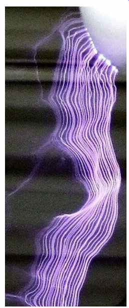
----- Electrical breakdown in an electric discharge showing the ribbon-like plasma
filaments from a Tesla coil.
The term electrical breakdown has several similar but distinctly different meanings. The term can apply to the failure of an electric circuit. Alternatively, it may refer to a rapid reduction in the resistance of an electrical insulator that can lead to a spark jumping around or through the insulator. This may be a momentary event (as in an electrostatic discharge), or may lead to a continuous arc discharge if protective devices fail to interrupt the current in a high power circuit.
Electrical system failure The most common meaning is related to automobiles and is the failure of an electric circuit or associated device resulting in a loss of vehicle function (a breakdown). Common problems include battery discharge, alternator failure, broken wires, blown fuses, etc.
Failure of electrical insulation
The second meaning of the term is more specifically a reference to the breakdown of the insulation of an electrical wire or other electrical component. Such breakdown usually results in a short circuit or a blown fuse. This occurs at the breakdown voltage. Actual insulation breakdown is more generally found in high-voltage applications, where it sometimes causes the opening of a protective circuit breaker. Electrical breakdown is often associated with the failure of solid or liquid insulating materials used inside high voltage transformers or capacitors in the electricity distribution grid. Electrical breakdown can also occur across the strings of insulators that suspend overhead power lines, within underground power cables, or lines arcing to nearby branches of trees.
Under sufficient electrical stress, electrical breakdown can occur within solids, liquids, gases or vacuum. However, the specific breakdown mechanisms are significantly different for each, particularly in different kinds of dielectric medium. All this leads to catastrophic failure of the instruments.
Disruptive devices A disruptive device is a device that has a dielectric, whereupon being stressed beyond its dielectric strength, has an electrical breakdown. This results in the sudden transition of part of the dielectric material from an insulating state to a highly conductive state. This transition is characterized by the formation of an electric spark, and possibly an electric arc through the material. If this occurs within a solid dielectric, physical and chemical changes along the path of the discharge will cause permanent degradation and significant reduction in the material's dielectric strength. A spark gap is a type of disruptive device that uses a gas or fluid dielectric between spaced electrodes. Unlike solid dielectrics, liquid or gaseous dielectrics can usually recover their full dielectric strength once current flow (through the plasma in the gap) has been externally interrupted.
Mechanism
Electrical breakdown occurs within a gas (or mixture of gases, such as air) when the dielectric strength of the gas(es) is exceeded. Regions of high electrical stress can cause nearby gas to partially ionize and begin conducting. This is done deliberately in low pressure discharges such as in fluorescent lights or in an electrostatic precipitator.
Partial electrical breakdown of the air causes the "fresh air" smell of ozone during thunderstorms or around high-voltage equipment. Although air is normally an excellent insulator, when stressed by a sufficiently high voltage (an electric field strength of about 3 x 10^6 V/m), air can begin to break down, becoming partially conductive. If the voltage is sufficiently high, complete electrical breakdown of the air will culminate in an electrical spark or arc that bridges the entire gap. While the small sparks generated by static electricity may barely be audible, larger sparks are often accompanied by a loud snap or bang. Lightning is an example of an immense spark that can be many miles long. The color of the spark depends upon the gases that make up the gaseous media.
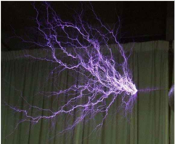
--- Electric discharge showing the lightning-like plasma filaments from a Tesla
coil. If a fuse or circuit breaker fails to interrupt the current through a
spark in a power circuit, current may continue, forming a very hot electric
arc. The color of an arc depends primarily upon the conductor materials (as
they are vaporized and mix within the hot plasma in the arc). Although sparks
and arcs are usually undesirable, they can be useful in everyday applications
such as spark plugs for gasoline engines, electrical welding of metals, or
for metal melting in an electric arc furnace.
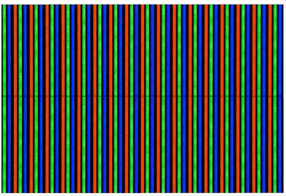
Voltage-current relation
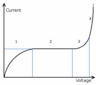
------ Voltage-current relation before breakdown
Before breakdown, there is a non-linear relation between voltage and current as shown in the figure. In region 1, there are free ions that can be accelerated by the field and induce a current. These will be saturated after a certain voltage and give a constant current, region 2. Region 3 and 4 are caused by ion avalanche as explained by the Townsend discharge mechanism.
Corona breakdown
Partial breakdown of the air occurs as a corona discharge on high voltage conductors at points with the highest electrical stress. As the dielectric strength of the material surrounding the conductor determines the maximum strength of the electric field the surrounding material can tolerate before becoming conductive, conductors that consist of sharp points, or balls with small radii, are more prone to causing dielectric breakdown.
Corona is sometimes seen as a bluish glow around high voltage wires and heard as a sizzling sound along high voltage power lines. Corona also generates radio frequency noise that can also be heard as 'static' or buzzing on radio receivers. Corona can also occur naturally at high points (such as church spires, treetops, or ship masts) during thunderstorms as St. Elmo's Fire. Although corona discharge is usually undesirable, until recently it was essential in the operation of photocopiers (Xerography) and laser printers.
Many modern copiers and laser printers now charge the photoconductor drum with an electrically conductive roller, reducing undesirable indoor ozone pollution. Additionally, lightning rods use corona discharge to create conductive paths in the air that point towards the rod, deflecting potentially-damaging lightning away from buildings and other structures.
Corona discharge ozone generators have been used for more than 30 years in the water purification process. Ozone is a toxic gas, even more potent than chlorine. In a typical drinking water treatment plant, the ozone gas is dissolved into the filtered water to kill bacteria and viruses. Ozone also removes the bad odors and taste from the water. The main advantage of ozone is that the overdose (residual) decomposes to gaseous oxygen well before the water reaches the consumer. This is in contrast with chlorine which stays in the water and can be tasted by the consumer.
Corona discharges are also used to modify the surface properties of many polymers. An example is the corona treatment of plastic materials which allows paint or ink to adhere properly.