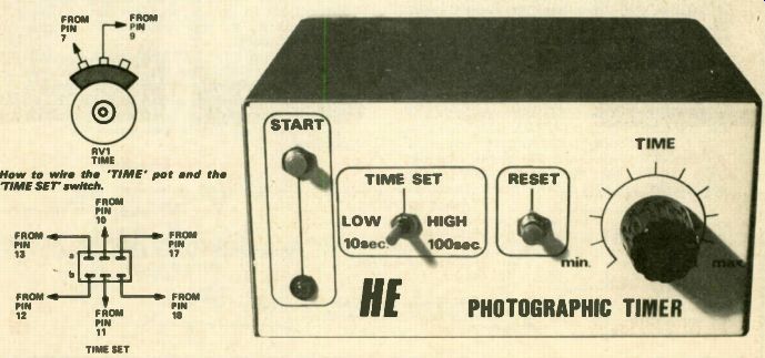
This project should appeal to the photo enthusiast. Use it to do your enlarger timing.
OUR PHOTOGRAPHIC TIMER is a useful project with some unusual features. It has two fully variable ranges, covering 0.9 seconds to 10 seconds and 9 seconds to 100 seconds. The unit has a relay output for turning the enlarger on and off, and is battery powered. Timing periods are initiated by pressing a start switch, and either end automatically at the end of the pre-set timing period, or they can be aborted part way through the timing period by pressing a RESET switch.
POWER SAVING
The most unusual feature of the timer is that it consumes power only during the actual timing period.
This feature makes it legitimate to use a battery power supply, which in turn increases the unit's versatility by making it fully portable and suitable for use as a general-purpose short--period timer. The unit has a built-in LED (light-emitting diode) that illuminates during the timing periods.
CONSTRUCTION
Most of the circuit is built on a PCB, and construction should present no problems if you follow the overlay with care. Be sure to fit the two diodes, the two electrolytic capacitors, the LED and the IC the right way round. Take extra care when doing the inter-wiring, especially to SW1.
If you wish to use the relay output socket we recommend, a 3 / 4 in diameter hole must be punched to house the socket. We used a Q-max metal punch for this purpose (available from most tool shops): this punch needs a pilot hole of 5/16 in.
When the construction is complete, double-check all wiring and then give the unit a functional check.
Connect the battery supply, press the START switch, and check that the relay and LED operate and turn off again automatically at the end of a pre-set period. The maximum timing period can be pre-set to precisely 10 seconds on range 1 via RV2, and to 100 seconds on range R via RV3.
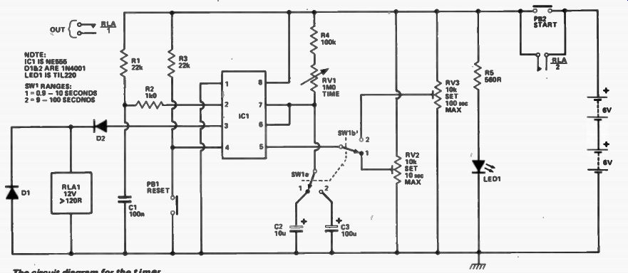
--------- The circuit diagram for the timer.
--------------
How it Works
The photographic timer is designed around a simple and inexpensive IC known as the 555 timer. Fig. 1 shows the circuit and waveforms of a simple manually-triggered timer built around this IC. Here, trigger pins 2 and 4 are normally held high by Ra and Rb, and output pin 3 is low.
When a brief negative-going trigger pulse is applied to pin 2 of the IC, via the push-button PBa, a timing period is initiated and the pin 3 output terminal immediately goes high and CI starts to charge towards the positive supply rail voltage via Rc.
After a delay determined by the values of Ca and Rc, the Ca voltage reaches 2/3 of the supply voltage value, and at this point a switching action is initiated within the IC in which output pin 3 switches rapidly to zero volts and Ca is discharged, thus completing the timing cycle.
Note that the timing cycle can be aborted part way through, if required, by applying a negative-going pulse (by briefly closing PB2) to pin 4 of the IC. Our photographic timer is a modified version of the basic Fig. 1 circuit. Look now at the full circuit diagram of our timer. Here, the output of the IC is used to drive relay RLA, which has two sets of N.O. (normally-open) contacts: one set of contacts is in series with the circuit's supply leads, and the other set is used to give output control. The circuit's START pulse is derived from the positive supply line via R1 and C1, and the timing periods are determined by the values of C2-C3-RV1-RV3-R4, which can be switch selected via SW1. The timer operation is initiated by momentarily closing PB2 and thereby briefly connecting the positive supply to the circuit. At the instant that the supply is connected, C1 is discharged: Consequently, trigger pin 2 is held negative relative to the supply line at this instant, and a timing cycle is immediately initiated: As the timing cycle is initiated relay RLA operates and contacts RLA /2 close and bypass switch PB2, thus maintaining the supply connection to the circuit once PB2 is released. At the end of the timing cycle RLA turns off and contacts RLA /2 open, thus breaking the supply connections to the circuit. The circuit thus consumes no current when it is in the STANDBY mode.
Pre-set pots RV2 and RV3 are switch-selected to connect to modulation pin 5 of the IC, and enable timing periods to be varied over a limited range to compensate for variations in the actual values if electrolytic capacitors C2 and C3 and to enable precise maximum timing periods to be obtained.
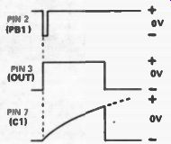
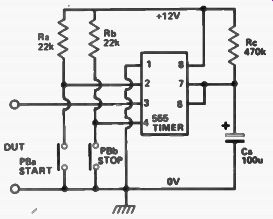
Fig. 1. The waveforms on the left are those produced by the simple circuit
on the right.
----------------
Above: The overlay for the PCB.
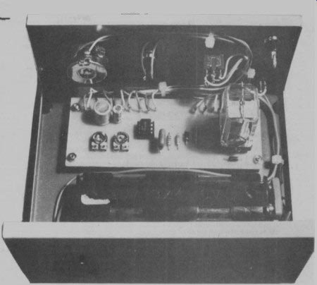
Above : Inside the box.
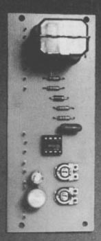
Top: The PCB with components in place.
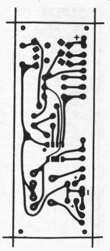
Top: The PCB foil pattern show full size
----------
Parts List
RESISTORS (All 5%. 1 / 4 W)
R1 22k
R2 1k
R3 22k
R4 100k
R5 560R
CAPACITORS
C1 100n (0.1uF) polyester, mylar etc
C2 10u 16V electrolytic, PCB mounting
C3 100u 16V electrolytic, PCB mounting
POTENTIOMETER
RV1 1 MO linear. Rotary
SEMICONDUCTORS
IC1 555 (NE555)
D1, D2 1N4001 silicon diode
LED1 TIL 220
MISCELLANEOUS
SW1 Miniature toggle, two pole, two way P61, PB2 Push button switches. push-to-make Relay 12V coil with minimum resistance of 120R, sub miniature type with at least two 'normally open' contacts (change-over contacts will contain a normally open pair)
PCB--Pattern as shown
Bulgin mains plug and socket, 2-off HP7 4 section battery holders. 8-off HP7 battery
Caseto suit.
(adapted from: Hobby Electronics magazine, Mar. 1979)
Also see: