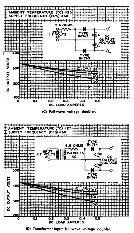
VOLTAGE DOUBLERS
Typical of silicon rectifiers that can be used for voltage-doubler service are the 1N1763 and 1N1764; their operation characteristics are given in these circuits.
Fig. A shows the type 1N1763 in a half-wave voltage-doubler circuit. As is characteristic with voltage doublers, the output voltage decreases as the current drain increases. The unloaded supply in this case has an output voltage of 300 volts DC; at 400 ma drain, the out put voltage has dropped to 250 volts using the smaller capacitor and to 270 volts using the larger capacitor.
Fig. B shows the type 1N1764 in a transformer-type half-wave voltage-doubler circuit. Here, with no load, the output voltage is about 425 volts; at 400 ma the voltage has dropped to 320 volts using the smaller capacitor and to 350 volts using the larger capacitor.
Fig. C shows the INI 763 in a full-wave voltage-doubler circuit fed directly from the line. With no load the output is 330 volts; at 400 ma the output voltage is 240 volts to 260 volts, depending on the size of the output capacitor used.
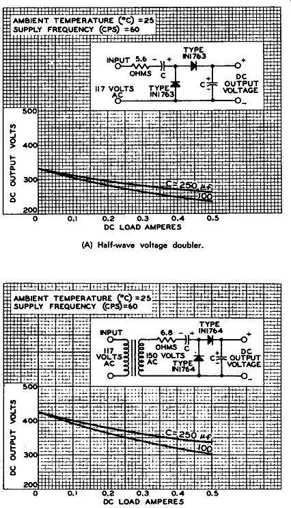
----- Four typical voltage doubler.
(A) Half-wave voltage doubler.
(B) Transformer-input half-wave voltage doubler.
(C) Full-wave voltage doubler.
(D) Transformer-input full-wave voltage doubler.
Fig. D shows a 1N1764 in a full-wave voltage doubler using a transformer. The unloaded output voltage is 420 volts, while the loaded output voltage at 400 ma is 310 volts to 370 volts, again depending on the size of the capacitor used.
VOLTAGE MULTIPLIER
This circuit is the equivalent of a vibrator circuit as used with an automobile battery to obtain d-c voltages for operating mobile radio equipment or audio amplifiers in an automobile. In this circuit the source voltage is shown as 1.5 volts, but the output voltage and current can be changed by varying the battery voltage and the transformer turns ratio. This is a typical circuit.
Two power transistors are used as an oscillator which operates as soon as the switch is closed. The step-up transformer provides an a-c voltage across the secondary; this voltage is rectified to produce a 50-volt d-c output.
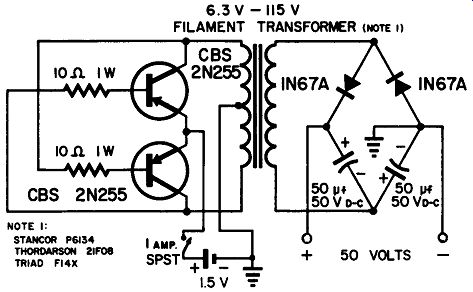
----- Voltage multiplier.
BATTERY CHARGER
A regulated 12-volt battery charger designed to be used with a 12-volt automobile battery is shown. The circuit is set for the required current to be sent through the battery. When the battery is fully charged, the charging current ceases. This circuit can be used with emergency power-supply sinks. If the battery is connected to the circuit and it becomes discharged while it is connected, the charger will switch back into the circuit automatically.
As shown, there is a full-wave rectifier using two silicon diodes across the 24-volt a-c secondary, with controlled rectifier SCR1 connected in series with the battery. If the battery voltage is less than 12 volts, there is a gate signal applied to SCR1 by means of resistor R2 and diode CR2. With this gate signal applied to the controlled rectifier, the rectifier conducts on each cycle of the supply voltage, and current flows until the battery is charged.
As the battery voltage approaches its normally charged value, capacitor C1 is sufficiently charged to turn on the second semi conductor-controlled rectifier ( SCR2) through zener diode CR 1.
When this point is reached, the voltage at point A, which is the gate of SCR1, suddenly drops to a value below the battery voltage. SCR1 cannot turn on, and the battery charging stops at this point.
With a fully charged battery connected to the circuit, R1 is set so that the charging just ceases. This resistor, or control, is known as the trip-point selector.
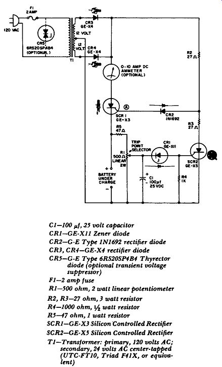
---------- Battery charger.
C1-100 uf, 25 volt capacitor
CR1-GE-X11 Zener diode
CR2-G-E Type JN1692 rectifier diode
CR1, CR4-GE-X4 rectifier diode
CR5-G-E
Type 6RS20SP4B4
Thyrector diode (optional transient voltage suppressor)
F1-2 amp fuse
R1-500 ohm, 2 watt linear potentiometer
R2, RJ-27 ohm, 1/2 watt resistor
R4-1000 ohm, ½ watt resistor R5-47 ohm, 1 watt resistor SCRJ-GE-XJ Silicon Controlled Rectifier SCR2-GE-X5 Silicon Controlled Rectifier
T1-Transformer: primary, 120 volts AC; secondary, 24 volts AC center-tapped (UTC-FTJO, Triad F41X, or equivalent)
------------- Selenium rectifier circuits.
Table 1. Selenium cell ratings.
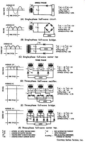
SELENIUM-RECTIFIER CIRCUITS
Six basic rectifier circuits and their characteristics are shown.
Fig. A is a single-phase half-wave rectifier used for low-power applications. There is a high ripple frequency which is the same frequency as the supply. The efficiency is relatively low.
Fig. B shows the single-phase full-wave bridge for a relatively high power with an efficiency of about 75%. The ripple frequency is twice that of the supply frequency, and this circuit makes greater utilization of the voltage available across the secondary.
Fig. C shows a single-phase full-wave center-tap circuit which re quires a transformer with a center tap and a terminal voltage of 2. 7 times the load voltage.
Fig. D shows a three-phase half-wave rectifier that can be used where low ripple is of primary importance. The ripple factor is about 20% and the ripple frequency is three times the fundamental frequency. The efficiency of this circuit is higher than the single-phase half-wave circuit.
Fig. E shows a three-phase full-wave bridge circuit that can be used where heavy d-c current is required. The ripple is very small, about 4 % , and additional filtering is often not required. This circuit has a d-c voltage output that is about 20% higher than the applied single-phase voltage.
Fig. F shows a three-phase full-wave center-tap circuit to be used where extremely heavy d-c currents are required. A transformer with a six-phase star secondary is needed, with each phase winding of the secondary provided with a center tap.
Suggested selenium cells for use with these circuits are shown in Table I, with the characteristics given for each cell for each circuit type.

SWITCHING REGULATOR
A switching type of voltage regulator is shown in block diagram form in Fig. A and in schematic form in Fig. B. The function of a switching regulator is to reduce the power loss in the series transistors when there is a large variation of the input or output voltage. A switching regulator operates on the principle that the output voltage is proportional to the input voltage according to the duty factor of the switch voltage.
There is a series control which is effectively a variable resistance feeding an output filter. The voltage output is compared to a reference, and then the error voltage or difference is used to adjust the duty cycle control. This feeds a driver that in turn adjusts the series control resistance.
The amplifier stage is made up of a differential amplifier and a stage of current gain; Q1 and Q2 make up the differential amplifier, while Q3 is the stage for additional gain. The purpose of the differential amplifier is to sense the output voltage and compare this to a reference so that the difference voltage can be amplified. The amplified error voltage is applied to the base of transistor Q3 which controls the charging rate on capacitor C3. A zener diode D1 provides a stable voltage source used for a reference, while zener diode D2 provides an offset voltage for the reference and differential amplifier. This allows the output voltage to be variable from 0 to 20 volts. Without this offset voltage, the minimum output voltage would be the reference voltage.
-------------- Switching regulator.
(A) Block diagram. (B) Schematic diagram.
------ (C) Circuit wave shapes.
(D) Load regulation.
R1-120 ohm, ±1% R2-500 ohm, 10-T potentiometer R3 -5 ohm potentiometer R4-2.2K, ± 1 % Rs, R•-100 ohm, ±1% R7-12K, ±1% R8 -10K, ±1% R9-2.7K, ± 1 % R,o, Ru, R16, Ru-4.7K, ±5% R11, R14, Ru-100 ohm, ±5% R12-150 ohm, ±1% R, s, R24-330 ohm ±5% R1 7-5.6K, ±5% Ru, R21-1.8K, ±5% R19, R20, R11-1K, ±5% R22-470 ohm, ±5% R2•-36K, ±5% R27-1 OK potentiometer R21-330 ohm, 5 watt, ±5% R29-20 ohm, ±5% R3 o, R3 1-0.1 ohm, 5 watt, wirewound R32-47 ohm, ±5% Ru-2 ohm, 5 watt, wirewound R34-100 ohm, 10 T potentiometer R35-40 ohm, 50 watt, wirewound R36-100 ohm, 5 watt, wirewound All resistors are ½ watt unless otherwise specified.
C,-12,500 mfd, 75V C7-0.006 mfd C2-0.001mfd Ca-50 mfd, 25V C3-0.003 mfd C4-0.05 mfd Cs-2200 pf C6-.01 mfd D,, D2-1N823A D3, D4, Ds-1 N4001 D6 -1N3128 D7-1N3889 a,, a2, a4, a., Q7-2N697 a.-2N2800 Qs, Qa-MU970 Q9, Q,o, Q11-2N2832 C9-2000 mfd, 75V C,o-0.1 mfd C11-SO mfd, 15V All capacitors are ± 10%. Q,2-2N2043 SCR-1-MCR 914-111-8 mh at 10A dc. Triad C-49U V1-45V ±5V at 10 amps peak with a 50% duty cycle V2-20V ±5% at 75 ma v.-2ov ±5% at 25 ma
-------- Switching regulator. (Cont)
Transistors Q4 through Q5s provide the duty-cycle control circuit.
Unijunction transistors Q5 and Q8 provide a relaxation oscillator for duty-cycle control and for frequency control. The oscillators produce pulses to trigger a bistable multivibrator circuit. Os controls the operating frequency of the regulator at 5 -khz. Transistor Q5 sets the "on-off" duty cycle of the 5 khz rate by generating pulses at time intervals which depend on the rate of charge of capacitor C3. Transistor Q4 discharges capacitor C3 at the beginning of each trigger pulse, thus resetting the charge on this capacitor from zero at the beginning of each cycle. Transistors Q6 and Q7 constitute a bistable multivibrator; pulses from the unijunction circuits trigger this multivibrator to produce variable duty-cycle pulses. Diode D3 provides bias for the transistors.
Power transistor Q9 is used as the driver circuit which is driven into saturation by the collector current of Q7. Saturating 00 causes the series switching transistors to be biased "off" due to the charge on capacitor C11.
Transistors Q11 and Q10 are the series switching resistors operating in parallel; they are biased "on" through resistor Ra5 and turned "off" by the driver transistor.
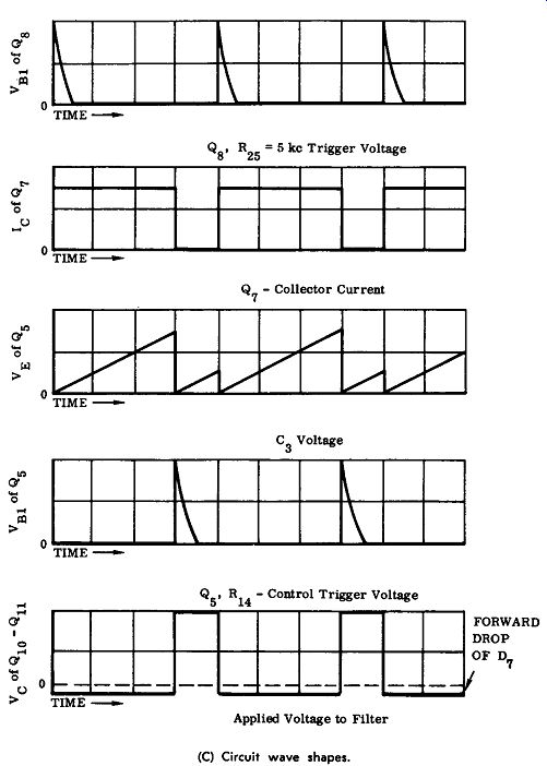
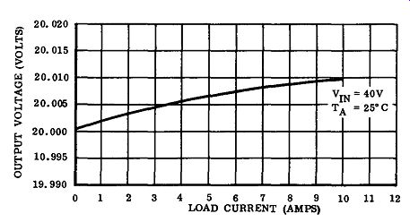
Circuit waveshapes are shown in Fig. C, and the load regulation for this circuit is shown in Fig. D. This load regulation from no-load to full-load is 0.05 % .
ELECTRONIC RIPPLE FILTER
It is possible to use transistor circuits to reduce the ripple in a power-supply filter, but these circuits are not designed to take the place of ordinary inductance and capacitance filters. They are designed to supplement the ordinary filter to produce very low values of ripple. For a circuit such as this to operate efficiently, it is necessary to reduce the ripple to an approximate value of 3 volts peak to-peak or less, ahead of the electronic filter.
Consider Fig. A as the basic electronic ripple-filter circuit which can be redrawn as an emitter follower as shown in Fig. B. The emitter follower, or common-collector circuit, is degenerative, and any in crease in voltage at the input will cause a decrease in voltage across the load so that the ripple is effectively reduced by the degeneration process. Another name for this circuit is the capacitance multiplier.
Suppose that in Fig. B a ripple voltage appears which would add to the 31 volts shown. This ripple voltage would have a tendency to increase the voltage across the load resistor, but note that the polarity of the increase will actually cause the base of the transistor to become less negative with respect to the emitter. This has a tendency to turn off the transistor, and the ripple voltage subtracts from the d-c power supply so that, in effect, any increase in voltage caused by the ripple will be effectively counteracted.
In Fig. A the capacitor shown in the circuit will try to maintain a nearly pure d-c voltage just as a battery would in the circuit. How ever, the capacitor has the advantage over the battery in that it can change its d-c voltage level, if required by the input voltage level.
Fig. C shows a circuit that will reduce the ripple by about a factor of 250 to 1 so that if the ripple is reduced to about 250 millivolts (peak to peak) by the inductance and capacitance filters ahead of the circuit, the output from this electronic filter circuit will only contain approximately 1 millivolt of ripple peak-to-peak.
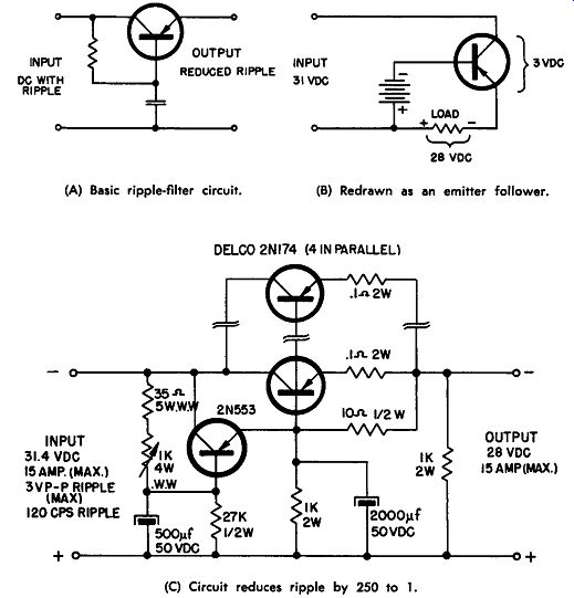
-------------- Electronic ripple filter. (A) Basic ripple-filter circuit.
(B) Redrawn as an emitter follower. (C) Circuit reduces ripple by 250 to 1.
PLUG-IN SILICON RECTIFIERS AS TUBE REPLACEMENTS
It is possible to replace vacuum-tube rectifiers with a direct plug-in replacement made from individual silicon rectifiers. These rectifiers and the tube type for replacement are shown in Table 2. For example, to replace a 5AU4 tube, a 1N2389 is suggested.
Table 2. Silicon-rectifier replacements for tubes.
ELECTRONIC RIPPLE FILTER
This circuit shows a simplified electronic ripple filter operating basically on the principle of a common-collector or emitter-follower circuit where the degeneration in the circuit effectively reduces the ripple coming from the power supply.
This electronic ripple filter is connected in a circuit so that the input to the filter is the output of the conventional inductance and capacitance filter. This circuit will reduce the ripple by about 6 to 1, as shown, and requires only three transistors.
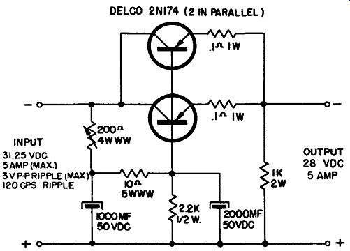
--------------- Electronic ripple filter.
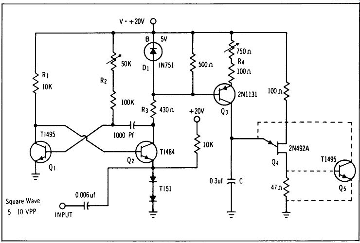
STAIRCASE GENERATOR
This circuit is a staircase waveform generator using a unijunction transistor to reduce the number of circuit components. The circuit can generate a staircase waveform at the emitter of unijunction transistor 2N492A, and it can also divide the input frequency by any desired ratio.
As shown in the circuit, a negative input pulse through transistor
02 turns this transistor on for a period of 15 microseconds as determined by resistor R2. A pulse from this conduction provides the drive for diode D1 and transistor Q3, which together provide a cur rent source controlled by resistor R_.. Capacitor C, as shown, is charged by this current source. The particular voltage at each step is determined by the value of resistor R-1, and when the voltage across capacitor C reaches the firing potential of the unijunction 2N492A transistor, the unijunction will fire and discharge the capacitor. This discharge produces a positive output pulse across the 4 7-ohm resistor connected to the unijunction; the output pulse is greater than 5 volts with a rise time of about 5 microseconds.
It is possible to feed input signals up to 10 -khz into this generator.
If transistor Q5 is added to the circuit, it will discharge capacitor C at a faster rate and double the maximum frequency of operation to about 10 -khz. Low-frequency operation is determined by the amount that the capacitor is discharged by the leakage path, which consists of transistor 0 3 , 0 4 and Q5. Waveforms that contain from 5 to 25 steps may be obtained by adjusting R4. With the various combinations for R2 and ~ there is a wide variation in the number of steps across capacitor C, and the maximum and minimum frequency rates may be determined by adjusting resistor R2 in this circuit.
------------
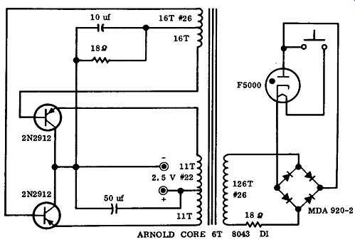
------------ Portable ultraviolet light source.
PORTABLE ULTRAVIOLET LIGHT SOURCE
This circuit shows a pair of 2N2912 power transistors operating from a 2.5-volt source as a portable ultraviolet light source using an F5000 gas tube. This circuit provides 400 ma at 26 volts. The two transistors act as a dc-to-ac converter, and the full-wave bridge rectifier connected to the secondary provides the necessary d-c for the ultraviolet light source. Operation of the converter is at about 8 -khz.
ELECTRONIC FUSE CIRCUIT
This circuit shows an electronic fuse used to protect power transistors. It is designed to be used from a 7- to 12-volt 5-ampere regulated power supply, and when the load in this case reaches 5.5 amperes, the transistor will open the circuit.
With the application of supply voltage V1 to the circuit, transistor Q1 is saturated by the drop across resistor R3. Load current will cause a voltage drop across resistor R1 which is in the positive leg of the circuit; when this voltage reaches about 0.8 volt, the diode D1 and transistor Q2 will begin to conduct as shown.
Conduction in Q2 causes the base of Q1 to be driven more positive, and when the collector of Q1 is sufficiently negative so that D2 can conduct, transistor Q2 will switch on completely and at the same time transistor Q1 will be turned off.
It is possible to reset the circuit by removing the short or excess load and by opening the reset switch momentarily. It is also possible to reset the circuit by removing the power for a moment.
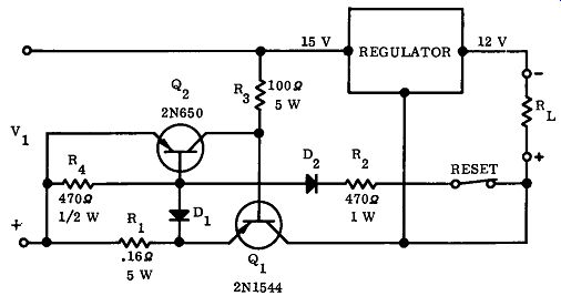
-------------- Electronic fuse circuit.
SILICON RECTIFIERS AS TUBE REPLACEMENTS
There are cases where it is desirable or necessary to replace vacuum tube diode rectifiers with silicon rectifiers. The silicon rectifiers will provide a longer life, they will withstand more physical damage than vacuum tubes, and they take up less room so that a circuit can be miniaturized. It is possible to make a direct substitution for vacuum tube or gas-tube rectifiers with silicon rectifiers by observing certain precautions.
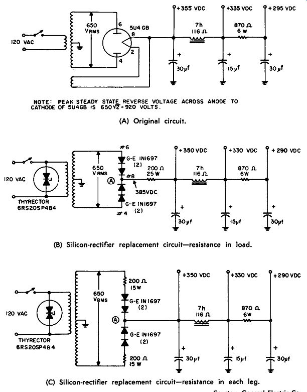
----------------- Silicon rectifiers as tube replacements. (A) Original
circuit. (B) Silicon-rectifier replacement circuit-resistance in load. (C)
Silicon-rectifier replacement circuit-resistance in each leg.
The voltage output of the circuit will increase because the voltage drop of the silicon rectifier is less than that of the vacuum tube or a gas tube. A silicon rectifier will, in general, provide about 10 volts more output than a gas or mercury rectifier, and as much as 50 volts more than the voltage output of a vacuum-tube rectifier.
The increased voltage of a silicon rectifier over a gas or mercury rectifier is normally not a problem in the circuit, but when substituting a silicon rectifier for a vacuum-tube rectifier, the increased voltage output must be compensated for to prevent damage to the circuit which is connected to the power supply.
Fig. A shows a typical vacuum tube, a 504GB full-wave rectifier in a power supply; Fig. B of the circuit shows a silicon rectifier re placement with the addition of a 200-ohm resistance to compensate for the increased voltage output; Fig. C shows the additional resistance used in series with the rectifier diodes themselves.
Essentially, the value of this extra load resistance is determined by the characteristics of the tube itself. It is necessary in a particular circuit to find the voltage drop across the tube at the required cur rent output. Using this voltage and this current the tube resistance under these conditions may be calculated, and the load resistance is approximately equal to this value of tube resistance. The power handling capability of the resistor is important, and when the cur rent and the resistance are known, the required wattage rating can be calculated. A safe value of wattage, preferably several watts greater than the required value, should be used.
Another consideration is that there is no warm-up time with a silicon rectifier, and if d-c voltage from the power supply is immediately applied to the vacuum-tube plates in the associated amplifier or other circuit, the vacuum tubes may be damaged. In many types of vacuum-tube equipment, a rectifier tube with an indirectly heated cathode, such as a 6X4 or 35Z6, is used so that the rectifier tube will have approximately the same heating characteristics as the amplifier tubes. If a silicon rectifier is used to replace a vacuum rectifier with an indirectly heated cathode, a time-delay relay or time-delay switch should be used in the circuit; under these circumstances a silicon rectifier can be used in place of an indirectly heated cathode vacuum tube rectifier. In the circuits of Figs. B and C transient voltage suppressors are suggested to prevent excessive voltage from appearing across the silicon rectifier.
-----------------
-----------------
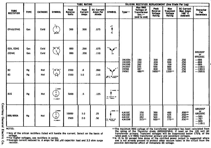
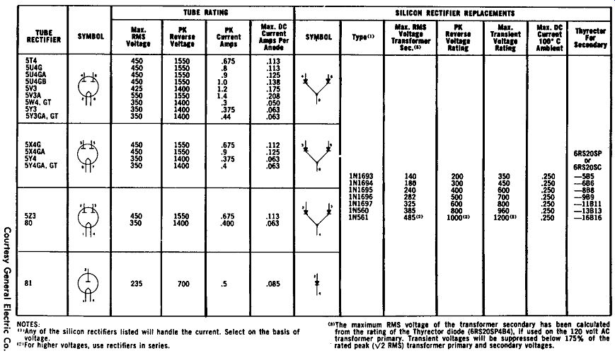
Table 3 shows some suggested silicon rectifier replacements for directly heated vacuum-tube rectifiers. Table 4 shows some silicon rectifier replacements for gas or mercury-vapor tube rectifiers. For example, the tube to be replaced is selected from the first column and its symbol or type is given in the second column. The tube ratings in terms of maximum voltage, peak-inverse voltage, peak current in amperes, and maximum d-c current in amperes for each plate is shown in the tables. The silicon rectifier replacements are direct replacements for the tubes as shown. Where the peak inverse or reverse voltage of the circuit is greater than 1000 volts a single silicon rectifier diode is not recommended for direct substitution. It is possible, how ever, to use two or more silicon rectifiers connected in series to obtain any desired voltage. Note that in the original circuit in Fig. A the peak-inverse voltage is 920 volts, and because of this, two silicon diodes, type 1N1697, are suggested to replace the rectifier tube.
Using this technique it is possible to build up a series of rectifier diodes to almost any desired peak-inverse voltage characteristic of the series.