AMAZON multi-meters discounts AMAZON oscilloscope discounts
When an EMI problem occurs, the test or design engineer needs to approach the situation logically. A simple EMI model has three elements:
- There must be a source of energy.
- There must be a receptor that's upset by this energy when the intensity
of the electromagnetic interference is above a tolerable limit.
- There must be a coupling path between the source and receptor for the unwanted energy transfer. For interference to exist, all three elements have to be present.
If one of the three elements is removed, there can be no interference. It therefore becomes the engineer's task to determine which is the easiest element to remove. Generally, designing a PCB (printed circuit board) that eliminates most sources of RF interference is the most cost-effective approach (called suppression). The source of interference is the active element producing the original waveform. The PCB must be designed to keep the energy developed to only those sections of the assembly that require this energy. The second and third elements tend to be addressed with containment techniques. Illustration 1 (below) provides a breakdown of the relationship between these three elements and presents a list of items associated with each element.
 |
||
NATURAL
HUMAN-MADE
|
RADIATION
CONDUCTION
|
BIOLOGICAL
HUMAN-MADE
|
above: (Illustration 1) Items associated with the three elements of the EMI environment.
With respect to PCBs, note the following:
- Noise sources are frequency generation circuits, component radiation
within a plastic package, incorrect trace routing, ground bounce from
digital logic, and common-mode currents developed within an assembly.
- The propagation path
is the medium that carries the RF energy, such as free space or interconnects
(common impedance coupling).
- Receptors are devices that easily accept interference from I/O cables, or by radiated means, transferring this harmful energy to circuits and devices susceptible to disruption.
Generally speaking, a product must be designed for two levels of performance:
one to minimize RF energy exiting an enclosure (emissions), and the other
to minimize the amount of RF energy entering (susceptibility or immunity).
Both emissions and immunity are transmitted by radiated or conductive
means. This relationship is shown in Illustration 2 (below). In addition,
the engineer should realize that a product must be compatible within itself,
i.e., emission levels must not compromise the performance of sensitive
segments within the product. When dealing with emissions, a general rule-of-thumb
is:
The higher the frequency, the greater the efficiency of a radiated coupling path; the lower the frequency, the greater the efficiency that a conducted coupling path will cause EMI. The extent of coupling depends on the frequency of the circuit and edge rate transition of digital components switching ogic states and transfer mechanism.
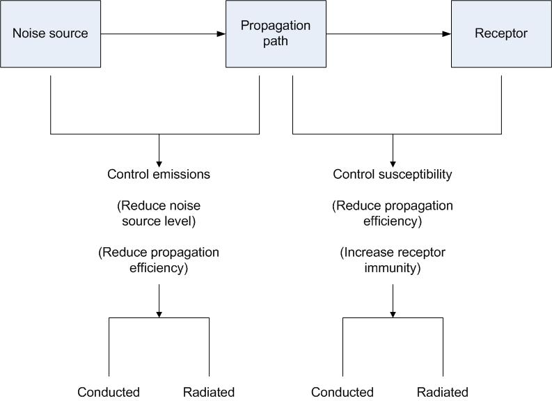
above: (Illustration 2) Variants of EMI coupling paths
top of pagePREVIOUS: The Basics of EMC | NEXT: The Basics of Electrical Interference