AMAZON multi-meters discounts AMAZON oscilloscope discounts
Diodes are the basic building blocks of ESD design. Diodes are used for ESD input node devices, mixed-voltage interface input environments, ESD rail-to-rail devices, and ESD power clamps. Diodes and gated-diodes serve as good ESD protection elements in many technologies: CMOS, radio frequency (RF) CMOS, BiCMOS silicon germanium, and silicon-on-insulator (SOI).
The key to good ESD design of diode structures is establishment of good current uniformity, establish internal ballasting, and avoidance of defect mechanisms that reduce the ESD effectiveness. Quantification of these design aspects can be achieved experimentally by the ESD results, simulation, or failure analysis. In this Section, we will discuss the design features of ESD diode structures for ESD networks.
1. ESD DIODE DESIGN: ESD BASIC
1.1 Basic ESD Design Concepts
FIG. 1 Physical layout design of a STI-defined diode structure
In ESD design of diode structures, there are some underlying fundamental concepts that one can adhere to in order to have effective ESD results. Diode ESD design have the following design objectives:
_ Provide a solution that establishes a low-voltage trigger element, which can discharge a high current.
_ Provide spatially uniform current density within the diode structure.
_ Avoid localized Joule heating.
_ Avoid electrical connections that exceed the breakdown voltage of the dielectric films.
_ Operate the device under the diode breakdown voltage.
_ Improve thermal stability of the diode structure.
The ability to provide a low-voltage trigger element can be achieved by the following means:
_ Use diode elements in the forward bias mode of operation to achieve low turn-on voltage.
_ Minimize the diode series resistance.
_ Minimize the number of diode elements in series.
_ Maximize the number of parallel diode elements.
High current can be achieved in diode ESD structures by the following means:
_ Low-resistance interconnects, via and contact structure and design.
_ Minimize the space between the anode and cathode regions.
_ Minimize the spacing between anode and cathode physical contacts.
_ Maximize the number of anode and cathode contacts that exist at minimum spacing.
_ Maximize the anode perimeter-to-area ratio.
_ Low-resistance salicide films on anode and cathode.
_ Heavily doped anode and cathode regions.
Spatial uniformity is achieved in the diode ESD structure by the following means:
_ Provide design spatial and electrical symmetry in the metal and contact design.
_ Ballasting perpendicular to the direction of the diode current flow.
Avoidance of localized heating in the diode structure can be achieved by the following means:
_ Provide design symmetry in the metal and contact design.
_ Introduce ballasting perpendicular to the diode current flow. (e.g., lateral ballasting) via design or semiconductor process.
_ Utilize vertical structures to avoid localized heating near the isolation surface.
_ Increase doping concentrations to increase the intrinsic temperature (Ti) and reduce the Joule heating of the diode regions.
Avoidance of failure of the diode structure in gated-diode structures due to dielectric breakdown can be achieved by the following means:
_ Avoid diode gate-to-power rail direct connections.
_ Avoid diode gate-to-pad direct connections.
Avoidance of diode thermal second breakdown and increase in thermal stability can be achieved by the following means:
_ Increase doping concentration of anode and cathode to increase the intrinsic temperature.
_ Reduce the IR voltage drop in the diode structure.
_ Minimize the Joule heating in the diode structure.
_ Avoid avalanche multiplication and electrical diode junction breakdown voltage.
1.2 ESD Diode Design: ESD Diode Operation
In the design of ESD diodes, the operation in high-level injection is key to its operation.
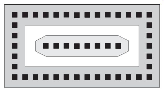
FIG. 1 shows an example of the physical layout of a shallow trench isolation (SIT) diode structure. In this figure p+ anode has chamfered corners, and is surrounded by STI structure.
The diode current equation in high-level injection can be expressed as […]
This expression reduces to the ideal diode case when the excess minority-carrier injection is small compared to the doping concentrations.
Diode resistance is critical in the understanding of the operation of a diode element during electrostatic discharge events. In a p+ /n-well diode structure, the anode resistance is a function of the contacts resistance, silicide film, and the p+ diode implant resistance. The design of the contacts and the silicide film play a key role in the forward-bias operation and the current density distribution of the diode structure. The cathode resistance (e.g., the n-well region+ is a function of the implant profile, the dose, and width of the physical well structure.
On the anode, the resistance can be expressed as…
…where the anode resistance is the resistance of the interconnect, the contact, the salicide film, and the anode implant. For the silicide film, the material, area coverage, and design of the silicide formed on the junction can alter the effectiveness of the silicide as well as the diffusion area on the ESD protection.
Equivalently, for the cathode, the cathode resistance is the sum of the resistances in series as well as the well resistance. For the cathode, typically the well resistance is the largest component of resistance which influences the ESD results.
From the diode equation, we can express the voltage across the diode as the sum of the voltage drops across the series resistance and the voltage drop across the metallurgical junction...
...where summation is over the voltage drops across the series resistances. The resistance can also be obtained from the derivative of the voltage with respect to current.
Solving for the resistance
From the high-level injection relationship,
Substituting in these expression, solving for the diode series resistance term as….
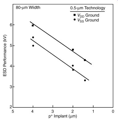
FIG. 2 ESD robustness as a function of width variation of the diode
structure
FIG. 3 Cartesian array of contacts in a ESD anode design
2. ESD DIODE DESIGN: ANODE
2.1 p+ Diffusion Anode Width Effect
In the design of the diode structures, the width of the p+ anode influences the ESD robustness of the diode design. Based on the diode equation under high-level injection, the current through the diode should increase proportionally to the area of the anode region.
But, if the summation term of the product of the diode current and internal resistance is significant, the operation will not be linear in the area. Note from…
Hence to design a diode to be effective and be proportional to the area, the voltage drops in the diode structure must be minimized. As a result, there is an anode width where this is satisfied. The internal resistance in the diode structure can be minimized using a high contact density, low sheet resistance salicide films, and interconnects that distribute the current effectively through the diode structure.
In the experimental work, using shallow trench isolation (STI) bound p+ anode diode structure, as the p+ implant anode area increased, the human body model (HBM) ESD failure level increased linearly, as shown in FIG. 2. In this case, the length-to-width ratio of the anode was varied from 100:1 to 50:1 (e.g., electrical connections were initiated perpendicular to the longer dimension).
From this experimental results, there is a design regime where the ESD robustness of the structure varies with the physical anode width.
2.2 p+ Anode Contacts
Placement of the physical contacts can influence the current in the anode and cathode regions under high current conditions. Non-uniformities in the current distribution lead to local non-uniform heating in the salicide film. The contact design layout can be formed in a Cartesian row formation or skewed. In a Cartesian row formation, the contacts are placed equally spaced in both the x- and y-direction side by side. In this formation, the maximum contact density can be placed on the ESD diode structure. FIG. 3 shows an example layout of the Cartesian contact configuration.
In an alternative contact design, the contacts are staggered so that each row or column is shifted. In this contact formation, the current uniformity is more evenly distributed. Kreiger proposed the staggered design concept to provide an improved uniformity in the structure.
FIG. 4 shows an example of a staggered or skewed contact design.
FIG. 4 Skewed (or staggered) rows of contacts for improved current uniformities
FIG. 5 Diode design with the silicide formation blocked at the edges
of the anode structure
2.3 p+ Anode Silicide to Edge Design
In many processes, such as LOCOS processes, where there is a concern that an ESD failure mechanism may occur at the triple point between the metallurgical junction, the salicide, and the isolation, ESD diode structure are designed to avoid formation of silicides near the anode-to-isolation edge. In LOCOS processes, etch processes can pull back the isolation structure, leading to the salicide formation being to close to the metallurgical junction. The LOCOS bird's beak effect can lead to a reduced space between the silicide and the metallurgical junction. In STI, STI pull-down can also make the silicide depth approach the metallurgical junction depth, decreasing the effective junction depth. This can lead to ESD-induced semiconductor process variation, reduced worst-case ESD robustness, and latent failure mechanisms. These type of ESD failures will be sensitive to salicide junction film thickness, and junction depth variations.
To avoid semiconductor process from causing early ESD failures, diode designs can be formed by preventing the silicide formation at the junction edges. FIG. 5 shows an example of a diode design with the silicide formation blocked at the edges of the anode structure. In this fashion, the silicide is formed under the complete diode area to provide a low-series resistance diode structure, and provide a good contact-silicide-contact resistance, but avoids the isolation edge issues. This can be achieved using a silicide block mask or any other mask, which occurs prior to the silicide formation process step.
2.4 p+ Anode to n+ Cathode Isolation Spacing
In the ESD design, the p+ anode and n+ cathode diffusion spacing are separated and defined by the isolation region. This isolation can be LOCOS or STI isolation regions. In the case of LOCOS isolation, as the spacing between the p+ anode region and the n+ cathode contact region decreases, the depletion region can be influenced by the spacing. In the diode structure, the p+ anode and n+ cathode contact regions extend below the isolation structure. A metallurgical junction is formed with a lateral p+ /n-=n+ junction. Hence, as the spacing decreases, it is anticipated that the breakdown voltage of the junction will decrease at small spacings.
In STI-defined diode structures, the doped regions do not extend below the isolation region. As the spacing decreases, the diode series resistance will decrease. Table 1 shows experimental results of an STI-bound diode structure as a function of isolation spacing. Based on the understanding of LOCOS isolation, a potential ESD degradation effect at small spacings was anticipated. From the experimental data, this was not evident in the design.
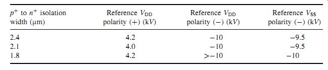
Table 1 HBM ESD robustness of a STI-bound diode structure as a function
of the isolation width
2.5 p+ Anode Diode End Effects
In p+ anode diode structures, end effects and end failure mechanism are evident in diode design. In a design where the p+ to n+ spacing is small compared to the lateral dimension, the current flow to first order will be two-dimensional. This assumes uniform current flow in the p+ anode structure perpendicular to its isolation interface. When the length is large relative to the spacing, this is a good first-order assumption. Along the length of the structure, the contact-to-STI space is uniform. At the end of the p+ anode diode structure, the last contact is equidistant from three edges on the side of the n+ cathode. In the case of the corners, current flows in three-dimensions introducing a three-dimensional effect and is the location of the failure mechanism. In LOCOS isolation, the metallurgical junction is cylindrical on the edges and spherical on the corners. In STI-defined diodes, the edges are planar surfaces, and the corners are cylindrical. At the STI-defined corner, the cylindrical region has a higher electric field. FIG. 6 shows the atomic force microscope (AFM) image damage of the corner of the diode structure.
To eliminate the three-dimensional effect, various ESD design solutions can be introduced:
_ Corner rounding of the p+ anode design using 45-degree chamfers instead of 90-degree corners.
_ Reduction of contact density in the n+ cathode contact.
_ Displacement of the last contact away from the p+ anode/STI edge.
_ Salicide removal on the p+ anode or n+ cathode contact.
_ Increase in the p+ anode to n+ cathode contact space (e.g., a wider STI region).
_ Increase the total number of diffusion fingers (e.g., total perimeter) to lower the total current density in any given region of the structure.
The first recommendation reduces the sharpness of the corner region. The other items increase the series diode resistance at the corner, which creates a closer matching of the resistance of the corner and the linear region. All the above items were experimentally introduced to eliminate the ESD failure mechanism. The most effective was the displacement of the last contact from the corner of the device. In this case, the current needed to flow through the salicide and p+ implant region to reach the n+ cathode contact. Prior to the elimination of the failure mechanism, the ESD failure introduced damage up to three contacts from the corner as well as salicide damage. By removing the last three contacts from the corner, this eliminated the failure mechanism.
Increasing the total perimeter and increasing the number of p+ anode fingers reduces the total current density in the structure as well as introduces more total number of corner regions. Instead of optimization of the corner region, the addition of many more corners and more total perimeter leads to a reduction of the total current density and the failure mechanism.
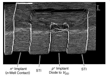
FIG. 6 Atomic force mapping (AFM) image of diode failure
As the diffusion width is scaled, the ability to chamfer the corners at 45 degrees is not possible in minimum width anode fingers. Hence, for minimum design width p+ anode regions, the designs must reintroduce 90 degree corners. Other features, such as the spacing of the last contact to the anode corner boundary, provide adequate resistance, so chamfering is not required.
2.6 Circular and Octagonal ESD Diode Design
Alternative ESD diode design are preferred to provide good ESD results and low capacitance. These include non-rectangular design layouts. Non-rectangular ESD designs can include waffle design, circular design, and n-sided polygons. Octagons are common by removal of the corners from a square shape. Non-rectangular designs have the following ESD advantages:
_ Lower current density due to the cylindrical and spherical current distribution.
_ Avoidance of isolation corner effects.
_ Placement in small areas where circles or octagons can be easily placed.
_ Self-enclosed structure avoiding isolation issues, wasted guard ring space, or adjacent structure parasitic interactions.
In the non-rectangular implementations, such as in a circular design, the ESD structure can consist of a center circle followed by concentric annulus of regions around the center region. The concentric circles can be anodes, cathodes, isolation, or guard ring structures.
The disadvantages of this design style are the following:
_ Design width and area limitations.
_ Computer-aided designs (CAD) issues exist with non-rectangular shapes (e.g., polygons, non-Euclidean orientations, octagons, and circle shapes).
_ CAD design automation convergence and process time.
_ CAD device and circuit model issues.
_ CAD-parameterized cells for non-rectangular shapes is not always possible.
_ Lithography and etch orientation issues.
_ Wiring limitations.
To avoid the design layout and CAD limitations, custom ESD designs are utilized with fixed sizes. These fixed design sizes require a custom device and circuit model.
3. ESD DIODE DESIGN: INTERCONNECT WIRING
The wiring of an ESD structure is critical to provide current uniformity and achieve a high ESD robustness per unit micron of structure area. The interconnect wiring in ESD design has the following roles:
_ Establish current density uniformity.
_ Establish a low diode series resistance.
_ Produce internal ballasting to self-limit current non-uniformities.
_ Avoid ESD design uniformities (e.g., corners, edges) from limiting the ESD robustness of the structure.
Various wiring strategies can be introduced into the diode design. Depending on the metal resistance, the contact resistance, the salicide sheet resistance, and the p+ anode sheet resistance, the different design patterns may or may not be successful. The metal pattern design can be of the following nature:
_ Parallel wiring.
_ Anti-parallel wiring.
_ Quantized tapered parallel and anti-parallel wiring.
_ Continuous tapered anti-parallel and parallel wiring.
_ Perpendicular (or broadside) wiring with center-fed design.
_ Perpendicular (or broadside) with uniform metal width.
_ Perpendicular (or broadside) wiring with H- and T-shape extensions.
3.1 Parallel Wiring Design
The ESD p+ anode and n+ cathode can be wired in a fashion where the current flows down the wire interconnect of the p+ anode (FIG. 7). The current then flows from the wire interconnect and then perpendicularly across the p+ anode to n+ cathode STI spacing. In the parallel wire configuration, the current then flows in a parallel fashion down the n+ cathode metal pattern, which runs the length of the n+ cathode; this is analogous to the MOSFET (as was discussed in the Section 3 on MOSFET current distribution). In this fashion, the ESD current flows from the left-hand-side of the end of the diode, and exits on the right-hand-side of the diode structure. In this design style, the anode or cathode can be mirrored forming a U-shape or horse-shoe design. This will lead to an unequal number of anode and cathode fingers.
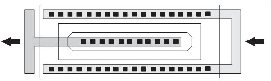
FIG. 7 Parallel wiring design
3.2 Anti-Parallel Wiring Design
The ESD p+ anode and n+ cathode can be wired in a fashion where the current flows down the wire interconnect of the p+ anode (FIG. 8). The current then flows from the wire interconnect and then perpendicularly across the p+ anode to n+ cathode STI spacing. In the anti-parallel wire configuration, the current then flows in a parallel fashion down the n+ cathode metal pattern, which runs the length of the n+ cathode, but exits the same side as it enters. For example, the ESD current flows from the left-hand side of the end of the diode, and exits on the left-hand side of the diode structure. In this design style, the anode or cathode can be mirrored forming a U-shape or horse-shoe design. For example, in an N finger p+ anode design, there may be N + 1 cathode fingers.
In the concept of parallel and anti-parallel wiring of an ESD diode, the ESD design forms a resistive-conductance (RG) transmission line down the length of the structure. The transmission line can be modeled as a series of resistor elements with diode elements between the top and bottom of the transmission line. The disadvantage of this implementation is that the voltage drops along the length introduce voltage non-uniformities.
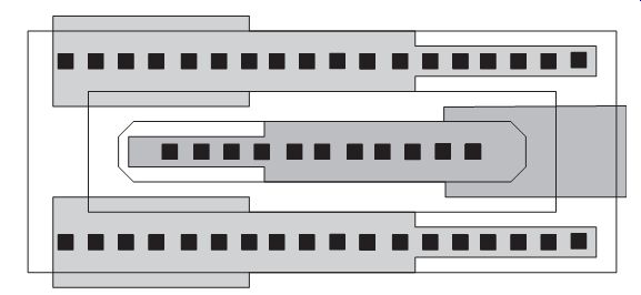
FIG. 9 Quantized tapered anti-parallel and parallel wiring
3.3 Quantized Tapered Parallel and Anti-Parallel Wiring
To minimize the voltage drops along the length of the parallel and anti-parallel configuration, the metal line at the cathode and anode can be widened incrementally along the length.
For example, the anode metal can be a given width at the electrical connection and incrementally tapers to a smaller width as the metal continues down the length. Equivalently, as the anode metal width is decreased, the cathode metal width increases, decreasing the voltage drop along the cathode metallization.
3.4 Continuous Tapered Anti-Parallel and Parallel Wiring
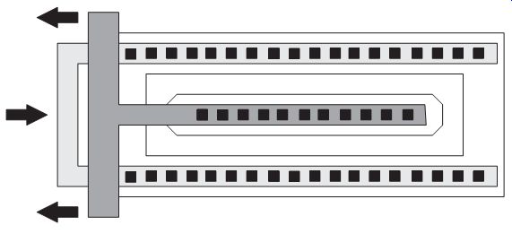
FIG. 8 Anti-parallel metal wiring design
In the above implementation, the wiring was tapered in a quantized fashion to maintain a piece-wise rectangular metal shape. The same concept can be introduced where the metal width is a uniform function of position (FIG. 10). In this case, the metal width is defined as W(x) where x is the position along the ESD diode anode finger. The advantage of this implementation is a more uniform solution and avoidance of discontinuities.
The disadvantage of these designs is the limited metal width, and at times significant voltage distribution drops along the structure. This can lead to a poor ESD robustness per unit micron of design area. In some cases, the design is limited to a given dimensional range of operation, and if the design remains in the dimensional space, no penalty is observed.
FIG. 10 Continuous tapered anti-parallel and parallel wiring
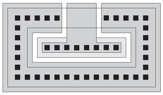
FIG. 11 Perpendicular (or broadside) center-fed ESD metal design
3.5 Perpendicular (or Broadside) Wiring with Center-Fed Design
In a perpendicular- or broadside-wiring pattern design, the ESD current flows from the pad to the ESD network along the width of the design (FIG. 11). The current flows in the same direction as the p+ to n+ cathode diode region. In a center-fed design, the input wire enters the left-hand side with the wide wire entering the center of the design. The current then flows to the n+ cathode, which is connected on the top and bottom of the cathode, and exits the right-hand side of the structure. The disadvantage of this design is that the current from the anode has difficulty flowing to the cathode structure, and the majority of the contacted p+ anode area needs to distribute the current perpendicular to the current flow to be near the n+ cathode area. This design can be improved by placing a first metal line along the anode and cathode and wire from the second level of metal. Again the disadvantage is that the current must now flow perpendicular along the first level metal to redistribute across to the cathode region. For high perimeter-to-area diode structures, this wiring design style has demonstrated significantly poor ESD robustness in advanced CMOS technology. An additional issue with this method is that there is no self-ballasting within the design due to the wide metal input shape and wide metal output shape.
3.6 Perpendicular (or Broadside) with Uniform Metal Width
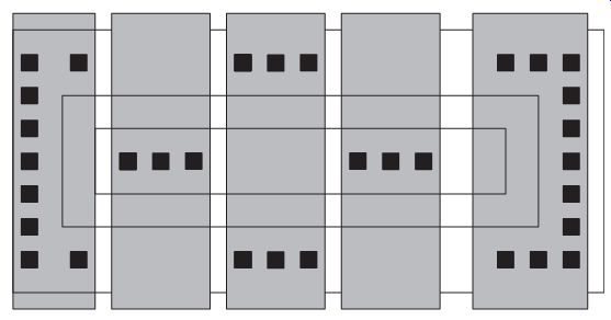
FIG. 12 Perpendicular (or broadside) with uniform metal width
In a perpendicular- or broadside-wiring pattern design, the ESD current flows from the pad to the ESD network along the width of the design (FIG. 12). The current flows in the same direction as the p+ to n+ cathode diode region. In this design implementation, the anode and cathode wiring is alternating across the design of a given width and space. The metal line can be a first or second level of metal. In the case of a single metal level, contacts are placed under either the p+ anode or the n+ cathode in an alternating fashion. In this design implementation, when the p+ anode interconnect passes over the n+ cathode, no contacts are placed on the n+ cathode and vice versa. In this fashion, the contact density is less than 50% coverage (e.g., no contacts exist in the metal line to metal line space). A first disadvantage of this design is that as the line width is wider, the spacing between the p+ anode and n+ cathode contact increases. In this design implementation, the best design is achieved by using a large number of narrow interconnect widths. To improve on the contact coverage, a first-level metal with full contact density can be placed on the anode and cathode fingers, with the contacting to the respective wiring is completed on a second-metal level. In this fashion, full contact density as well as a lower lateral resistance is achieved from the first-level metal. Again, the disadvantage is the current must now flow perpendicular along the first-level metal to redistribute across to the cathode region. In this design style, the M2 wiring and M1 wiring patterns introduce some self-ballasting within the design.
3.7 Perpendicular (or Broadside) Wiring with T-Shaped Extensions
In a perpendicular- or broadside-wiring pattern design with T-shape extensions, the ESD current flows from the pad to the ESD network along the width of the design (FIG. 13). The current flows in the same direction as the p+ to n+ cathode diode region.
In this design implementation, the anode and cathode wiring is alternating across the design of a given width and space. A distinction from the other design without the T-shape extensions, this metal design then introduces metallization lateral to the current flow. This wider metal level then allows to contact the p+ and n+ cathode region with a large number of p+ and n+ contacts at a minimum spacing between them; this produces the lowest lateral resistance and the highest ESD results. The metal line can be a first or second level of metal.
In the case of a single metal level, contacts are placed under either the p+ anode or the n+ cathode in an alternating fashion. Although the contact density is not 100% of the area, the number of minimum spaced p+ to n+ contact spacings is the highest. The ESD electro thermal damage patterns of molten silicon show that the damage occurs between the local anode and cathode contacts. This design can be further improved by introduction of either ''M-zero'' wiring (e.g., local interconnect) or a two-level metal design with 100% contact density.
3.8 Metal Design for Structures Under Bond Pads
The design of ESD diode structures under bond pads can be constrained based on the metallization design rules in a given technology. For structures under bond pads, the metal level and metal width may be constrained to avoid insulator cracking. In an interconnect system with aluminum metallurgy and silicon dioxide, large area regions of metal under insulators lead to the material deflection of the insulator above during loading from bonding processes. The insulator film can be modeled as a material beam with the two ends rigid. The mechanical bond pad load can be modeled as a uniform load along the length of the insulator region. In this case, the mechanical deflection of the film can be determined, with the maximum deflection occurring at the center of the bond pad. As the length of the bond pad increases, the deflection at the center also increases. When the material exceeds the maximum yield stress, cracking occurs in the insulator leading to material failure. The deflection is a function of the bond load, and inversely proportional to the second moment of inertia of about the material axis, and the elastic constant. Additionally, as the insulator film is farther from the region of mechanical loading (e.g., top surface), the lower is the likelihood of failure. As a result, the lower the metal level, the lower is the mechanical failure risk.
ESD designs under bond pads are at time constrained to given metal levels and pattern designs. In the case of aluminum interconnects, low-level metal films are suitable to avoid mechanical failure. Additionally, to minimize insulator deflection, no large area regions are used for metallization patterns. Many of the aforementioned design patterns are suitable. A metal pattern not suitable, for example, is the center-fed metal pattern, which introduces large area metal under the insulator regions.
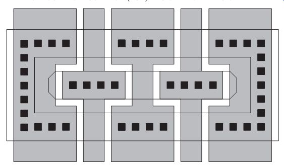
FIG. 13 Perpendicular (or broadside) wiring with T-shape extensions
4. ESD DIODE DESIGN: POLYSILICON-BOUND DIODE DESIGNS
Polysilicon-bound anode diode structures were introduced to avoid salicide issues in STI structures. Polysilicon-bound anode structures can be formed in two different fashions.
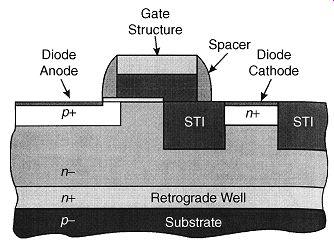
FIG. 14 Polysilicon-bound anode structure diode
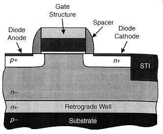
FIG. 15 Polysilicon-bound anode and cathode structure diode
A first structure introduced a polysilicon-bound anode structure where the polysilicon MOSFET gate structure overlaps the STI region to avoid the triple point formed between the p+ implant, the salicide, and the STI region (FIG. 14). Note in this structure, the n+ cathode contact remains bound by STI. This structure prevents the salicide from approaching the perimeter where the polysilicon MOSFET gate structure serves as a salicide-blocking mask. As the silicide is deposited, it extends over the MOSFET spacer and gate region, and not penetrating into the p+ silicon implant region. The role of the STI shape in this structure serves two purposes. The first purpose is to prevent the flow of surface currents. The STI region forces the current around the isolation to reach the n+ cathode contact. This forces the current to flow vertically through the heavily doped well region. The second purpose is to define the n+ cathode contact region.
In a second implementation, as shown in FIG. 15, the polysilicon MOSFET gate structure defines both the p+ anode and n+ cathode regions. The advantage of this structure is twofold. First, a higher density diode structure is achieved by elimination of the STI region. Second, the series resistance between the anode and cathode is reduced, since the current can flow laterally across the surface. Given that the surface current leads to high current density and current crowding, early ESD failure could occur. In the experimental results, there was no concern with this potential issue. In this fashion, the left-hand side of the structure has the p-channel MOSFET implants, and the right-hand-side of the structure has the n-channel MOSFET implants. A block mask is formed over the top of the structure to form the anode and cathode structure.
In this structure, all of the additional MOSFET implants are present in the ESD design.
This ESD design structure will contain low-doped drain (LDD), extension implants, and halo implants. These implants will influence the surface physics and capacitance near the surface of the device. Note that in this structure, the cathode region is either an n-well or p-well region. As a result, one of the halo implants is the opposite of the cathode region doping polarity. This extra resistance region can be eliminated to lower the ESD diode device resistance. In this implementation, there is a ''good halo'' and a ''bad halo.'' The good halo lowers the diode series resistance, and the bad halo counter-dopes the well structure. This polysilicon-bound diode structure can be formed as a p+=n-=n+ diode structure or a p+/p-/n+ diode structure.
4.1 ESD Design Issues with Polysilicon-Bound Diode Structures
In these polysilicon-bound diode structures, there are ESD design issues. The following ESD design issues exist with these diode structures:
_ Physical contact to the MOSFET gate structure in the enclosed gate region.
_ Choice of electrical connection of the polysilicon MOSFET gate structure.
_ Dielectric over-voltage of the polysilicon gate structure.
For the first item, the ESD design encloses the p+ anode with a polysilicon ring. Electrical contacts of gate structures are not used. Hence, to electrically connect to these gate structures, a STI island must be placed in the channel region. In this fashion, electrical contacts can be placed to electrically connect the structure.
A second issue is the electrical connection of the gate structure. The choice of electrical connection of the gate structure influences the loading, operation, and electrical overstress or ESD failure mechanisms. The gate structure can be connected to the anode, the cathode, power rails, or left floating. The over-voltage and ESD issues can be resolved using circuit solutions, which are less costly. In many technologies, allowing a gate structure to float is a concern for semiconductor manufacturing charging issues and antennae effects. As a result, the use of a floating polysilicon MOSFET gate structure in many technologies is not allowed.
For example, the polysilicon MOSFET gate structure can be connected to the n+ cathode region. In the case of a double-diode implementation, two polysilicon-bound diode structure can be used. A first polysilicon-bound diode structure is used between the input pad and the VDD power supply, whose anode is connected to the input pad and the cathode is connected to the VDD power supply. A second polysilicon-bound diode structure is placed where the cathode is connected to the input pad, and the anode is connected to the VSS power rail. In this implementation, as the input pad undergoes a voltage undershoot, the voltage across the top diode oxide region is VDD + Vunder, where Vunder is the undershoot voltage magnitude. As the input pad undergoes a voltage overshoot over the power supply voltage, the voltage across the gate of the lower polysilicon diode structure is VDD + Vover, where Vover is the overshoot voltage. In this implementation, the gate dielectric is overstressed during the overshoot event. Note that the diode voltage drop will limit the overshoot and undershoot events. If the sum of the diode turn-on voltage and the IR drop across the diode structure is less than the overshoot, the overshoot will be constrained by the structure turn-on. Hence, depending on the size of the overshoot current and the resistance of the ESD element, voltage clamping will occur from the ESD devices. But, as the oxide thickness scales, the allowed voltage across the dielectric will be limited.
5. ESD DIODE DESIGN: n-WELL DIODE DESIGN
A second diode structure of importance is the n-well diode used for negative discharging into the chip substrate. n-well ESD diodes extend below the surface isolation (e.g., ROX, LOCOS, or STI), making them insensitive to n-channel MOSFET source/drain dose and silicide penetration. n-well diode structures have been effective solutions for allowing ESD current to flow into the bulk chip substrate. n-well ESD design and the wiring pattern are significantly influenced by the substrate material and its doping concentration.
5.1 n-Well Diode Wiring Design
The wiring pattern in an n-well design with the electrical contact to the p- substrate contact can follow the same design pattern as shown with the STI-bound p+ anode diode structure.
_ Parallel wiring.
_ Anti-parallel wiring.
_ Quantized tapered parallel and anti-parallel wiring.
_ Continuous tapered anti-parallel and parallel wiring.
_ Perpendicular (or broadside) wiring with center-fed design.
_ Perpendicular (or broadside) with uniform metal width.
_ Perpendicular (or broadside) wiring with H- and T-shape extensions.
As was discussed in the case of the STI-bound p+ anode, similar metal design patterns can be implemented for the n-well cathode structure. The identical issues are present with these structures but there are some important differences:
1. The effectiveness of n-well diodes in both p- or p+ substrates is significant, leading to a lower perimeter requirement. This minimizes the need for a high number of multiple fingers and complex metal patterns.
2. The width of the n-well is limited by implant, diffusion, and process limitations. As a result, the width of the n-well regions are significantly wider than the minimum width formed from a STI-defined shape (e.g., n+ or p+ region). As a result, the metal width in these designs may not require tapering and other techniques.
3. In a p- epitaxial/p+ substrate wafer, the effectiveness of the substrate allows for no need for a surface electrical contact local to the ESD network.
Hence, the ESD effectiveness of these structures allows for a significant smaller perimeter and area with respect to the STI-bound p+ anode area. As a result, the bussing drops and multi-finger issues are reduced in these implementations. Experimentally, again the broad side center-fed n-well diode performance was significantly lower than the broadside wiring with T-extensions.
In a p- epitaxial/p+ substrate wafer, the substrate serves as a good electrical and thermal shunt for the ESD current. As a result, electrical connections to the substrate local to the n well diode structures are not necessary. As a result, there is no need to have VSS wiring planes or grids interwoven into the ESD design. Hence, this simplifies the metal pattern and prevents the need for integration of the VSS wires into the ESD diode network. In the case of the n-well diode, the anode region does not need to be electrically connected locally. Additionally, the ESD robustness of the diode structure in a p- epitaxial/p+ substrate wafer is 2_ superior to a low doped p- wafer.
As a result, the size of the structure is smaller, making it less of a need to introduce parallel, and anti-parallel connections with quantized steps, or continuous tapering. Experimental results with n-well diode structures in p- epitaxial/p+ substrate wafer demonstrated that ESD results were superior when there was no local STI-bound p+ contact electrical connection to VSS. It is postulated that the grounding of the VSS rail leads to local current crowding near the n-well diode structure, limiting the ESD robustness of the n-well diode structure. It is believed that a lower current density and less current crowding were achieved using the bulk substrate as the thermal and electrical current shunt during negative pulse ESD testing relative to VSS power rails.
In a p- substrate non-epitaxial wafer, a local p+ substrate contact can be introduced. As a result, the different metal patterns can be implemented for the n-well diode structure for the anode and cathode. This lessens the design freedom obtained in the case of the p+ substrate wafers. From experimental work, the ESD robustness of the n-well diode in a p- wafer is approximately 2_ lower. Hence to achieve comparable ESD robustness as achieved in a p- epitaxial wafer, the n-well diode structure will require double the design area. In this case, the total area of this structure is still significantly less than that needed for a STI p+ anode structure. As a result, the metal patterns can remain simple.
In the wiring decision, the choice of the wiring may be defined by the wiring channels and pattern used for the STI-bound p+ anode design. For example, in a double-diode implementation, using a STI-bound p+ anode diode and an n-well diode, the same metal pattern (e.g., metal width, level, and metal-to-metal space) may be used for both for wire ability.
5.2 n-Well Contact Density
In an n-well diode design, the width of the n-well is limited by the minimum n-well, which can be formed in a technology. Whereas in a STI-defined p+ anode, a minimum width can be utilized, and the n-well diode will be significantly wider. As a result, multiple rows of contact structures as opposed to a single row can be utilized without additional area penalty.
5.3 n-Well ESD Design, Guard Rings, and Adjacent Structures
In an n-well ESD design, the adjacent structures can influence the function of the n-well ESD diode. n-well diode structures are typically used for negative pulse ESD events. The negative pulse events lead to the forward bias of the n-well to p- substrate metallurgical junction. Holes from the substrate flow to the input pad, and electrons from the cathode flow into the p- substrate region. The anode resistance and the current distribution influence the effectiveness of the n-well diode structure. For the case when the power supply rail (e.g., VDD) is a ground reference, the electrons discharged into the p- substrate flow to the grounded reference. In many cases, n-doped regions are electrically connected to the VDD power rail.
Guard ring structures can be formed around the n-well-to-substrate ESD diode to collect the injected electrons in the substrate. When a semiconductor chip is powered, guard rings electrically connected to the VDD power supply, act as a collector of minority carrier electrons in the p- substrate during undershoot conditions. The n-well ESD diode, the p- substrate, and the n-type guard ring form a lateral parasitic bipolar transistor, where the n-well-to-substrate ESD diode serves as the emitter region, the p- substrate serves as the base region, and the n-doped guard ring structure serves as the collector region. The guard ring structure can be an STI-defined n-implant, n-well, or a triple-well isolation n-band region. The ability of the adjacent n-doped region to collect minority carrier electrons is a function of the collector depth, the width, the spacing relative to the n-well diode, the bias condition, and the substrate doping concentration and substrate lateral and vertical profile.
The guard ring efficiency to collect minority carriers should increase with increasing collector depth and width, and decreasing spacing between the guard ring and the ESD n-well diode. For example, an n-well guard ring will serve as a superior guard ring compared to the STI-bound n-diffusion due to the physical size and depth of the structure. In the design of the guard ring structure, the choice of the type of structure and the lateral spacing has a large role in its effectiveness.
For ESD events, the placement of the adjacent structure can modulate the ESD HBM robustness. Wafer-level ESD testing of an n-well ESD diode on a p- epitaxy/p+) substrate wafer demonstrated a decrease in the HBM robustness as the space between the n-well diode and an n-well guard ring structure decreased (FIG. 16). From an electrical perspective, the smaller base width should demonstrate an improved ESD result instead of an ESD degradation; but if the failure of the structure is a function of higher current density, self heating, and smaller physical volume, then it plausible that the ESD failure for the smaller spacing is logical and not counter-intuitive.
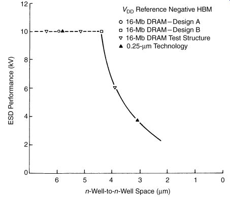
FIG. 16 ESD HBM results of an n-well diode as a function of the lateral
spacing to the n-well guard ring structure
In the physical design of the n-well guard ring structure, the STI-defined n-diffusion serves as the electrical contact to the well structure, and a maximum contact density is used to allow for a low resistance collector region. When low contact density is used, or one-sided electrical connections, the effectiveness of the collector structure is degraded.
In ESD designs, when an n-well guard ring is not placed around an n-well ESD diode structure, negative pulse events from chips, cards, cables, or systems can lead to minority carrier injection, leading to reliability concerns. These concerns can consist of MOSFET threshold shifts, noise, or latchup. Additionally, for negative mode ESD testing relative to the VDD power supply rail, poor ESD results can occur if there is no defined current path to the VDD power rail.
Utilizing adjacent structures that contain circuitry (e.g., n-well tubs connected to VDD power rails) can also play a role of a region to act as a guard ring or discharge path to the VDD power supply.
This can save chip area in ESD design but the following design practices must be followed to be effective:
The spacing of the n-well ESD diode relative to the adjacent structure and the guard ring should be symmetrically matched to provide uniform current flow to both the adjacent structures on both sides of the ESD n-well diode.
Elements contained in the adjacent structure must be electrically connected or spaced to avoid potential parasitic pnpn initiation (e.g., CMOS latchup).
An ESD n-well diode can be formed with a guard ring structure on one side, and an n well tub on the other side. From a design symmetry perspective, the spacing between the ESD n-well diode relative to the n-well tub and the n-well guard ring is equal. In this fashion, the two lateral bipolar npn base widths and areas are matched preserving symmetry.
Electrically, the two n-well regions also are connected to the same power supply rail. On the second issue, although the parasitic pnpn is physically present, the electrical connections are not in such a fashion that latchup can be initiated within the structure. In this case, the p+ n-well diode is electrically connected to the n-well ESD diode. The electrical connections are such that the lateral pnpn anode and pnpn cathode are electrically connected. From the experimental damage patterns, the molten silicon can be observed symmetrically from the n-well ESD diode to both the n-well guard ring structure and the interior n-well tub.
6. ESD DIODE DESIGN: n+/p SUBSTRATE DIODE DESIGN
In an n+/p- substrate diode ESD design, the same issues and characteristics as discussed for the n-well/p- substrate apply to the n+ diode region. There are some ESD design distinctions between the n-well ESD diode and the n+ diffusion diode. The n+ diffusion ESD diode is sensitive to the isolation structure. The isolation structure will influence:
_ Silicide penetration.
_ Breakdown voltage.
_ Lateral thermal dissipation.
n-well ESD diodes extend below the surface isolation (e.g., ROX, LOCOS, or STI), making them insensitive to n-channel MOSFET source/drain dose and silicide penetration.
No special silicide masks are needed for n-well diode structures. In n+ ESD diode structures, these can be sensitive to the MOSFET source/drain dose and energy, refractory metal species, silicide thickness, hot process, and the isolation lateral or vertical control (e.g., LOCOS lateral bird's beak and STI pull-down mechanisms).
As a result, in LOCOS-defined n+ diffusion ESD diodes, silicide blocking masks can be placed to reduce the sensitivity of silicide penetration into the metallurgical junction from LOCOS pull-back or vertical silicide penetration. Three different silicide masking designs can be used:
_ Silicide block mask at the isolation edge.
_ Silicide block mask of the n+ diffusion except under the contacts.
_ Full silicide block mask of the full n+ diffusion.
In the first case, the blocking of the edge reduces the sensitivity of the LOCOS- or STI isolation issues. In the second case, the vertical penetration risk of refractory metals into the metallurgical junction is reduced, yet contact resistance is maintained. In the third case, no salicide is formed on the structure. The disadvantage of the last case is an undesirable higher contact resistance.
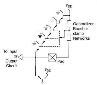
FIG. 17 ESD diode string design highlighting vertical pnp transistor
and generalized boost network
7. ESD DIODE DESIGN: DIODE STRING
Where voltage differential needs to exceed a diode voltage, series diodes are the basic building blocks of ESD design for ESD input node devices, ESD rail-to-rail devices, ESD power clamps, ESD trigger elements, and circuit elements. Series diodes or ''diode string'' configurations introduce some unique device design, circuit, and integration issues.
The key to ESD series design of diode structures is
_ Utilize parallelism of adjacent diode elements in the chip or system design.
_ Optimize the successive stages for area to provide minimum loading and the maximum ESD current discharge.
_ Reduction or elimination of the vertical parasitic bipolar effects on the turn-on voltage and leakage.
_ Eliminate any parasitic interaction between adjacent diode elements.
_ Minimize total diode series resistance.
_ Minimize the number of diode elements in series to the minimum product application requirement.
On the issue of parallelism, the ability to integrate series diodes of successive stages from adjacent signal pads, groups of adjacent signals, and peripheral ''banks'' has a significant impact on the design area and the ESD robustness result. A second means of area and ESD optimization is the area optimization within a given signal pad. Optimization of the area of each successive stage allows for some advantage of providing lower capacitance and area reduction as well.
A unique aspect in the ESD series diode configurations is the vertical bipolar parasitic effects and the interactions between adjacent structures. FIG. 17 shows an example of an ESD diode string circuit. The role of the vertical bipolar transistor influences the turn-on voltage, the ''on-resistance'' as well as leakage amplification. The diode equation can be simply represented for a diode within the string as…
In the on-state, the saturation current can be neglected. From the form above, the forward voltage of the ith stage can be represented as…
In a p+ /n-well ''diode'' string, in a p- substrate dual-well technology, a vertical pnp transistor exists. The collector current can be represented as…
...and the base current can be represented as…
In a series configuration, these form a common-collector configuration. The base of each stage is connected to the emitter of the successive stage. A set of equations exist, which can be represented in the form…
Given a set of m diodes, where we define first to equal the current ID, the successive diodes are a function of the product term […]
For example, given m = 5
From the above result, it is clear that the amount of current flowing through each successive stage decreases. As the pnp bipolar current gain is much less than unity, the current through the successive stages is approximately equal. In the case when the vertical pnp bipolar current gain is greater than unity, some percentage of the current flows to the substrate and some current flows along the length of the successive diode stages. In the case when the bipolar current gain is small compared to unity, the majority of the current…
flows through the successive diode stages. In a diffused well technology, the vertical bipolar current gains typically exceeded unity value (e.g., bipolar current gains exceeded 10). In retrograde well technology, typically the bipolar current gain was well below 10. In many advanced CMOS and BiCMOS technologies, the vertical bipolar current gain approached unity values.
7.1 ESD Design: Diode String Current-Voltage Relationship
A key parameter of the series diode configuration is the turn-on voltage, VT. The diode string turn-on voltage can be represented as the sum of the forward-bias voltages.
Using the forward voltage expression, we can express this as…
Assuming that the diodes are at the same local temperature, the thermal voltage term can be achieved through the summation sign. Replacing the diode current for the ith diode, the above relationship can be expressed as …
In this form, it can be observed that the m-diodes in series are equal to the summation of the forward voltage plus an additional term. The turn-on voltage is a function of the number of diodes in series, the forward voltage of each diode, the area parameter, and vertical bipolar current gain. Assuming equal areas of each diode, this can be expressed as…
The significance of this expression is that the turn-on voltage is not the sum of the forward-diode voltages but modified by the second term. In the case that the second term is zero, the operation of the network works as ideal diodes, as if there was no parasitic vertical bipolar element. Hence in the limit that the bipolar current gain approaches zero, the equation approaches an ideal diode representation…
A second key aspect of the turn-on equation is that each successive diode has less effectiveness. For example, given a diode string of m + 1 diodes, the representation can be shown as [...]
As the number of diodes increases, the net forward voltage with the addition of more elements is less effective with each additional element, since the second term decreases the net gain in the turn-on voltage. This decrement is also a function of temperature in the thermal voltage and the bipolar current gain.
A third key aspect of the turn-on equation is that the pnp bipolar current gain modulates the turn-on voltage. Different semiconductor processes will have different turn-on characteristics for a common design. FIG. 18 is a plot of the turn-on voltage as a function of the number of diode stages for two different processes, which have different bipolar current gain. For example, a LOCOS-defined junction with a diffused well will have a pnp bipolar current gain on the order of 10 to 30. In a STI-defined diode structure with a retrograde well, the bipolar current gain can be below 10. As the doping concentration of the semiconductor process well increases, the bipolar current gain will decrease.
In the simple case of equal area diodes, we can evaluate the change in the turn-on voltage, assuming a first and second bipolar current gain.
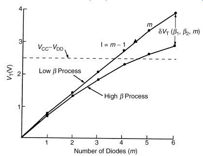
FIG. 18 Turn-on voltage as a function of stage number for two different
semiconductor processes of a first and second bipolar current gain
The turn-on voltage difference can be expressed as [...]
In the reverse-biased condition, the turn-on voltage will be a function of the diode and bipolar breakdown voltage conditions. Assuming the base of the last diode stage is at ground potential, and the substrate floats, the voltage drop will occur that can be simplistically assumed as the sum of the reverse breakdown voltage between the p+ anode to n-well cathode breakdown voltage
VTr= mBVeb = mVrev
This is valid when the breakdown voltage remains below the vertical bipolar breakdown voltage of any given stage. At each stage, when the product of the number of stages times the emitter-to-base breakdown voltage exceeds the n-well-to-substrate breakdown voltage or the BVCEO (e.g., open base collector-to-emitter voltage), the breakdown will occur between that stage and the ground potential. Current will flow to the substrate for each successive stage beyond this point.
A second key parameter in the analysis of a series diode string is the effective series resistance. A simple analytical model for the effective series resistance demonstrates its dependence on n-well sheet resistance and the bipolar current gain. An a.c. common collector model can be defined for the diode string network. Using a hybrid-_ model, the pnp transistor can be represented as an emitter resistor, re, a current source, _ib, and base resistance. The impedance, Z, looking into the first stage is…
In the common-collector configuration, the emitter resistor is in series with the base resistor in the series diode ESD network. If the emitter resistor is small compared to the base resistance, this can be neglected. In a p+/n-well network, the base resistance is a function of the well contact resistance and the n-well sheet resistance. Evaluation of the total impedance…
Solving Kirchhoff's current law at each successive node in the circuit, the current through each successive stage is lower than the prior stage by the current gain factor.
The effective impedance (e.g., resistance) can be represented as …
If the n-well resistance is much larger than the emitter, contact, and interconnect resistances, we can assume that the majority of the stage resistance is related to the n-well sheet resistance...
From this, we can express the effective impedance of the ESD network as …
Given that each successive stage is equal in design length and width, the expression can be represented as an effective sheet resistance [...]
This formulation which highlights the effective resistance of the ESD diode string structure is a function of both the n-well sheet resistance and the parasitic bipolar current gain. The ESD device effectiveness decreases with increasing n-well sheet resistance for processes with low bipolar current gain. Assuming the limit that the bipolar current gain approaches zero, the effective resistance approaches the sum of the diode resistances. In the case of high n-well sheet resistances, the bipolar current gain will also increase. As a result, the lower current gain term lowers the effective resistance term leading to an improved ESD diode string structure effectiveness.
To show the effect of the bipolar current gain on the sheet resistance, we need to establish a relationship. Assuming a relationship between the vertical bipolar current gain where the bipolar current gain is proportional to a power of the well sheet resistance, expressed as ...
...where we assume n is a positive number. From this expression, the impedance can be expressed according to the following relationship.
FIG. 19 shows the effective resistance as a function of well sheet resistance. When the pnp bipolar current gain is negligible, the effective resistance is linearly proportional to the n-well sheet resistance and the slope is proportional to the number of stages (as well as the width-to-length ratio). As the bipolar current gain increases, the effective resistance separates from the ideal resistance asymptotes and converges to a single-stage asymptote. As the effective resistance curves separate from the ideal asymptotes, the circuit is transitioning from being a diode-dominant to a bipolar-dominant operation.
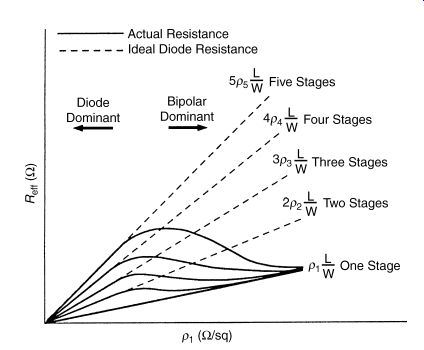
FIG. 19 Effective resistance as a function of n-well sheet resistance
and the number of diode stages
7.2 ESD Design: Diode String Design-Architecture and the Design
7.3 Diode String Elements in Multiple I/O Environments
Signal pin spatial and electrical placement is a function of the chip design and architecture.
The placement of the signal pin, power pins, and power rails is a function of the floor planning of the chip design. Diode string ESD design can take advantage of these elements to provide improved ESD design. Diode string ESD design can introduce parallelism to improve the individual pin results. This can be achieved by the following:
_ Introduction of sharing of successive diode stages between adjacent signal pads.
_ Introduction of metal strapping between local diodes.
_ Introduction of metal rails between diode stages to connect adjacent signal pads.
_ Introduction of voltage power pins.
Sharing of the diode strings can lead to an improved ESD protection and area reduction.
Sharing of the diode strings cannot be done at the first diode element, but can be initiated after the first stage of a diode string design. In this fashion, the second stage and all future stages can be integrated. One means of integration is the second stage of adjacent element which is the same silicon diode element. A second means of integration is that they are independent diode elements which are then electrically connected to a common element. A third mean is instead of a local connection, a metal rail or bus is established across a grouping or bank of elements. A fourth means is to provide a separate power pin and electrically connected all signal pins globally to this physical pin. In this case, all successive elements become a series between the global new power pin and the nominal power rail.
As shown in the diode string development, the effective impedance (e.g., resistance) for each independent signal pin can be represented as…
If the n-well resistance is much larger than the emitter, contact, and interconnect resistances, we can again assume the majority of the stage resistance is related to the n-well sheet resistance
From this, we can express the effective impedance of the ESD network as ...
In the grouping of the signal pins, the first stage must be independent (e.g., the pins will be shorted together if we do not assume this case). Then in general, we can write...
For all stages after the first stage, the total width of the ''ith'' stage, can be a function of the number of parallel elements.
This assumes a dummy variable k, which runs from a single I/O element to n-parallel elements which are electrically connected. In the case that one diode is utilized for successive stages, the term reduces to a single width.
For the ith element, the summation of the parallel elements will determine the total width.
Given the same design style, we can assume the sheet resistance and the ''length'' are the same. The total effectiveness of utilization of the total width is a function of the ability to distribute or redistribute the current through the given stage or stage-to-stage. This is a strong function of the placement, spacing, and metal design patterns from signal pad to signal pad.
7.4 Integration of Signal Pads
FIG. 20 shows a set of diode string ESD designs. Each diode string is connected to an independent pad. In this case, the ESD designs are independent of adjacent elements. In this fashion, the effective resistance of each stage is higher.
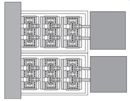
FIG. 20 Floor plan of adjacent I/O ESD designs
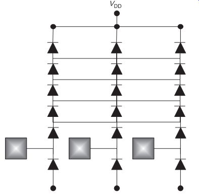
FIG. 21 Introduction of metal strapping between successive stages
This design can be modified with improved results by integration of all the successive stages after the first element. FIG. 21 is an example of the introduction of sharing of successive stages using metal connections. In this means, the signal book floor plan remains equivalent. As an example of the effectiveness, two designs were completed. The first design contained five-diode strings in a series configuration with no interconnection between adjacent signal pads. The worst-case ESD robustness of the 0.50-mm technology microprocessor was 3000 V HBM levels. In the redesign of the chip, in the next technology generation, the ESD area was reduced by 50% due to the need to integrate a cascode p-channel OCD element. By introducing of the sharing of the diode elements using metal straps across adjacent cells, with 50% of the ESD area, the improvement increased from 3 to 10 kV HBM ESD levels. From this result, it is clear that the reduction of the series resistance in the successive stages significantly reduced the effective impedance in the implementation.
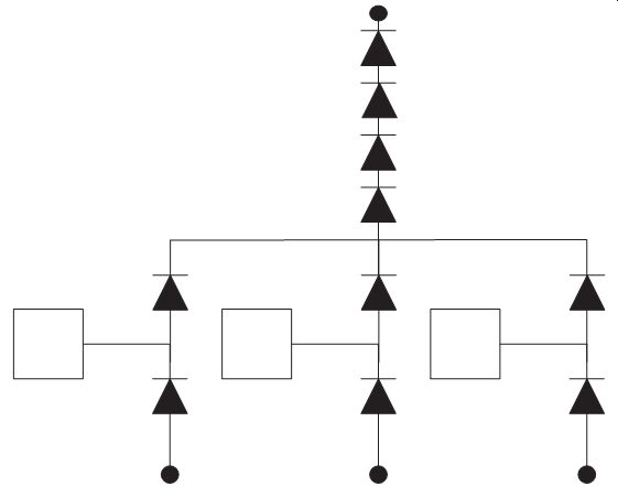
FIG. 22 Introduction of a common diode region for successive stages.
In a second design practice, the successive diode string stages can be integrated in silicon as a common element across adjacent signal pads. FIG. 22 is an example where the second stage and all successive stages are connected to a common silicon region.
In a second example implementation, four signal pads were placed in a ''nibble architecture.'' In that implementation, because of the narrowness of the pad pitch, the first stage diodes were placed perpendicular to the pad layout. The second and successive stages were rotated 90 deg to the first stage, and straddled the four signal pads. In this fashion, the successive stages were four times the pitch of the individual signal pads and integrated across all four signal pads. In order to have the current flow from the first stage to successive stages, metal was introduced to redistribute the current into the second and successive stages. The worst-case ESD results achieved over 6000 V HBM levels in a very small physical area. The interesting result was the area utilized was equal to a single non-mixed voltage application in the 0.35-mm MOSFET channel length technology that achieved only 3000 V.
Additionally, the design modification can be established where new bus rails can be placed to redistribute the current across the larger elements (FIG. 23). This bus can be local to the connected signals, or continue to all signal pads. In the case where it is connected to a group or all signal pads, this can be connected to a larger dummy ESD bus, or a dummy signal pin.
From this integration design strategy, it should be clear to the reader that the successive stages do not have to be local to the signal pins. For an n-stage ESD diode design, the successive stages from i = 2 to i = n, can be spatially separated from the signal pin and placed in a separate region of the design. These can be placed near the chip corners, power pads, service functions, or other design locations. The effectiveness will be a function of the bussing resistance, current distribution, and redistribution between the successive elements.
As these elements are integrated from signal to signal, the area dedicated to a signal pad begins to migrate from a local pin ESD protection to serving and assisting the global chip ESD protection.
7.5 ESD Design: Diode String Design-Darlington Amplification
Leakage, photo-emission, and noise can be a concern in ESD diode elements.
In the ESD diode string configuration, the collectors of the successive stages are in a common-collector configuration. The n-well region cathode is contained within the chip substrate region. This n-well region contains a metallurgical junction between the substrate and the base region. Minority carrier injection, photo-generation, or signals that are transmitted at the n-well to substrate junction can be propagated through the diode string configuration. Because of the diode string electrical connections, the collector of the successive stage is the base region of the prior stage. All signals on the collector region is then amplified in the prior stage. The diode equation can be simply represented for a diode within the string as [...]
In the on-state, the saturation current can be neglected. In the case that the diode is not in forward active mode, the diode current is [...]
FIG. 23 Introduction of dummy ESD bus rails into the diode string design
In the diode string configuration, the pnp bipolar base current is amplified by each successive stage (from the end of the diode string back to the first stage) when each stage is in a forward active mode of operation. Each stage amplifies the base current by the reverse ...
pnp bipolar current gain, _r
For five diodes in series, assuming the leakage is coming from the last diode only…
In this fashion, the injection at every collector region is then propagated to the first stage.
Leakage or minority carrier generation is then current amplified through each successive stages. This can be represented as a summation expression. As a result, the total reverse current is a function can be assumed to be equal to…
From this expression, the leakage amplification can be estimated as the product of the bipolar current gain of the successive stages (or simplified as beta to the power of the number of stages) and the reverse current seen on the last stage
The amplification is a function of the ...
_ Area of the collector-to-substrate junction of each diode stage.
_ Area of the p+ anode region.
_ Reverse bipolar current gain.
_ Diode (base) series resistance.
_ Magnitude of the forward bias state.
In the case of a Darlington amplifier, it is well known that if each successive stage increases in the physical size, the total current increases. As the diode elements get larger toward the input node, the amplification current will increase. Hence, to eliminate the amplification effect of a diode string element, there are some basic design and process choices
_ Reduce the vertical pnp bipolar current gain using heavily doped retrograde well implants, sub-collectors, or buried layers.
_ Maintain the area of the successive stages as equal, or increase the size of the diode area from the input to the power supply.
_ Reduce the total number of diode stages.
_ Prevent forward biasing across as many stages as possible in the given application.
In an m-stage ESD diode string design, the Darlington amplification of the leakage current follows the relationship…
The first means is to lower the bipolar current gain of each successive stage. One method to reduce the vertical bipolar current gain is to apply this circuit in a technology that can introduce features that lower the parasitic bipolar current gain characteristic. In early CMOS processes, n-well structures were formed using diffusion processes. In these processes, the vertical bipolar gain ranged from 10 to 30. In that case, the amplification of the leakage was increased as 10m, where m is the number of stages. In these technologies, the power supply voltages ranged from 3.3 to 5 V VDD levels in CMOS applications, and 12 V for non-volatile RAMs (NVRAMs). In these cases, the number of series diodes ranged from 5 to 10 diodes. In these cases, without an alternative solution, the circuits had significant leakage current. Additionally, in the case of flash NVRAM applications, the photon current would be amplified through the ESD network leading to noise spikes during flash operation.
Using retrograde well technology and sub-collector implants, the vertical bipolar current gain can be reduced, eliminating the magnitude of the reverse amplification. For example, in heavily doped retrograde wells, the bipolar current gain can be reduced to _ = 2. In this case, the leakage is amplified by a factor of 64. Hence as the bipolar current gain is reduced toward unity, the reverse amplification is not a significant issue.
Second to lower the amplification is to reduce the number of successive stages. As technology scales to lower power supply voltages, the number of diode elements in series will be reduced.
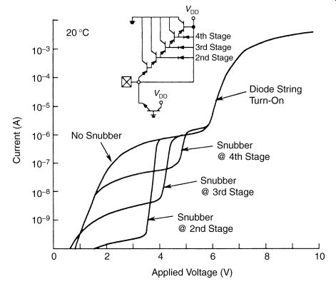
FIG. 24 Circuit simulation of the input pad current versus applied voltage
as a function of Snubber diode stage connections
An alternative strategy is to break the Darlington amplification effect by using circuit techniques instead of area optimization. Three circuit concepts exist:
_ Clamping elements across a number of stages to prevent forward bias condition for reverse amplification.
_ Boosting elements to prevent forward bias condition for reverse amplification.
_ Establish an alternative current path.
The clamping or boost elements concept can be achieved using passive or active elements. Resistors, diodes, or MOSFETs can be used to prevent the initiation of the reverse amplification effect.
FIG. 17 shows a generalized boosting and clamping network for an ESD diode string for elimination of Darlington amplification. The method of using a simple diode element was first proposed by Kirsch. The operation as an ESD diode string was demonstrated in conjunction with G. Gerosa. The diode (or vertical pnp bipolar element) was placed between the last stage of the ESD power clamp and a prior stage. The simplest solution was a diode element which was coined as an ''ESD snubber diode'' element. To break the Darlington effect of the reverse amplification, an additional ESD snubber diode was placed in the base of a bipolar stage. In essence, the ''snubber diode'' is a bipolar transistor between VDD and ground (VSS) potential whose base is connected to one of the diode stages.
Circuit simulation was used to determine the most effective location of the ''ESD snubber diode'' element to eliminate the leakage and not impact circuit functionality. FIG. 24 shows the circuit simulation results with the ''ESD snubber diode'' at different stages. In the figure, the case of the diode string without a snubber element is shown in a LOCOS/diffused well technology. In the figure, a large ''hump'' is evident below the turn-on voltage of the diode string element. The first ''hump'' in the I-V characteristic is associated with the Darlington amplification, and the second current increase is associated with the diode string turn-on voltage. The optimum clamping action was obtained by placing the snubber diode on the second stage. The snubber diode boosts the second stage voltage to VDD + Vbe (e.g., one forward bias voltage drop from the power supply). When the voltage is boosted toward the power supply voltage, it clamps the forward voltage across the individual stages, which limits the leakage current amplification.
As the snubber element is placed toward the signal pad, the voltage at which the clamping occurs shifts to lower voltages. The optimum effectiveness was evident when the snubber element was connected to the base of the second stage.
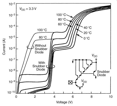
FIG. 25 Circuit simulation of input pad I-V characteristics of ESD structure
in a LOCOS technology highlighting Snubber clamp Darlington action clamping
as a function of temperature
FIG. 25 illustrates the circuit simulation of the pad leakage current with and without a snubber diode for the LOCOS/diffused well semiconductor process for different temperatures for the case where the snubber diode is placed on the second stage. The circuit simulation results show that, without the snubber clamp element, the leakage is significantly amplified at elevated temperatures below 3.3 V application voltages. When the snubber clamp element is in place, the leakage is reduced by 4-5 orders of magnitude Experimental measurements of the snubber diode ESD diode string circuit was demonstrated in a low- and high-bipolar pnp current gain process. FIG. 26 shows the same electrical circuit in two different technologies. In the low bipolar current gain retrograde well technology, there are a few key points of interest:
_ The snubber diode lowers the leakage by 1-2 orders of magnitude.
_ The turn-on diode string voltage is ''ideal.'' There are key issues to note in the case of the diffused well case:
_ The snubber element provided a 5 order of magnitude reduction of the leakage current at temperature in the high bipolar current gain technology.
_ The ''hump'' is still evident above a given voltage.
_ The turn-on voltage is lowered due to the vertical bipolar current gain.
In this implementation, for the high bipolar current gain diffused well technology, the Darlington amplification was significantly above a retrograde well technology. This was effectively reduced using the circuit solution. But the third issue is significant. In the two processes, the heavily doped retrograde well process has ''ideal diode'' turn-on voltage value whereas the diffused well process has a non-ideal condition. From an ESD perspective, the lower turn-on voltage allows for an earlier turn-on of this network. From a functionality perspective, the lower turn-on voltage leads to a higher input leakage current (note: this is not the amplification effect). In the application, the lower voltage increases the input current by two to three decades higher than an ''ideal diode string'' application. This is a concern for functional applications
7.6 ESD Design: Diode String Design-Area Scaling
In the ESD design of diode strings, based on the analysis of a diode string structure, the amount of current flowing through the successive stages is a function of the area of each stage as well as the bipolar current gain. The base of each stage is connected to the emitter of the successive stage. A set of equations exist which can be represented in the form
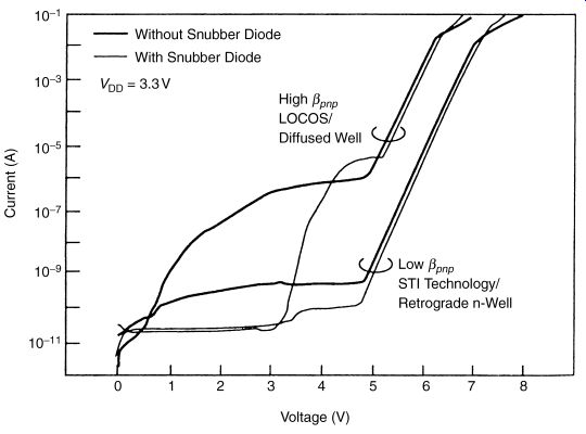
FIG. 26 Electrical characterization I-V characteristics of an ESD diode
string with and without a Snubber diode for a low- and high-bipolar current
gain technology
[...]
In this design strategy, the area of the stages increase with each stage to carry a constant current through a physical size. This has an advantage in that the first stage is the smallest stage. In this case, the capacitance is lowest near the signal pad. FIG. 27 shows an example of a diode string with successively larger diode stages.
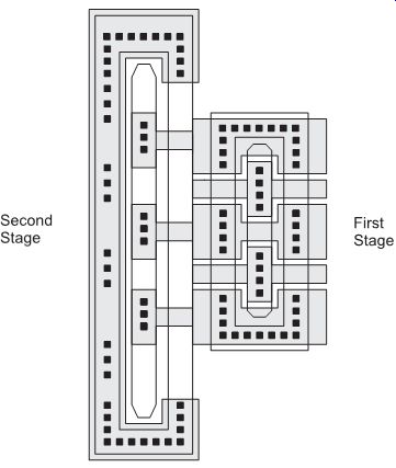
FIG. 27 Diode string design with successively larger area diode stages
8. ESD DIODE DESIGN: TRIPLE-WELL DIODES
Triple-well technology allows for the isolation of both p-channel and n-channel elements.
To form an isolated p-region separate from the p-substrate region, a dopant layer of opposite type is introduced. An n-type dopant layer is placed under the p-well region to isolate the epitaxial region. On the edges of the structure, insulators or metallurgical junction are formed to isolate the physical region. On the edges, shallow trench isolation (STI), trench isolation (TI), or deep trench (DT) isolation can be used to intersect the epitaxial region to fully isolate the region [32].
With the introduction of the triple-well structure, the ESD diode elements are modified.
The structural distinctions are the following:
_ A vertical npn bipolar is present between the n+ diffusion diode, p- isolated epitaxial region, and the n-type buried layer.
_ A vertical pnp element of a p+ diffusion in a p- isolated epitaxial region, the n-buried layer, and the p- substrate.
_ An n-well diode will be modified by the n-type buried layer, or cannot be used (e.g., abutting of the layers).
_ An n-p diode can be formed between an n-diffusion within the isolated p- region, and the p+ substrate contact to the p- region.
As a result, the operation of the physical elements will differ in that new parasitic elements are introduced. Utilization of these elements will be a function of the doping concentrations, physical depths, spacings, and electrical connections. The electrical connection of the n-buried layer (e.g., power supply choice, circuit connection, or floating state) will influence which ESD mode of operation this element will be active in. In triple-well technology, triple-well input node ESD networks can be constructed between the signal input node and the power supply voltage VDD, as well as elements between the signal pad and the chip substrate or VSS power rail.
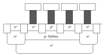
FIG. 28 Triple-well ESD power clamp with p+ diffusion in an isolated
p-well and n-band second cathode.
In single- and dual-well CMOS series diode ESD power clamps, the p+ /n-well elements, the parasitic bipolar element exists between the p+ diffusion, the n-well, and the substrate region. The successive diode stages are in a pnp common-collector configuration. For negative polarity ESD events, n-well-to-substrate diodes and n-diffusion-to-substrate diodes are used between the signal pad and the electrical ground.
Triple-well CMOS and BiCMOS technologies allow for a buried n-type layer to be placed in a fashion to isolate the p-epitaxial region or p-well region. The separation of the epitaxial layer from the substrate allows for design symmetry between the signal pad and the power supply rails (e.g., VDD and VSS).
A triple-well ESD input network can be formed using a p+ anode in a p-well, with an underlying buried layer implant. Isolated epitaxial regions can be formed using an implant layer or sub-collector implants from bipolar transistor elements. The ''edge'' structure, to isolate the epitaxial region, can be a diffused region (e.g., n-well) or a trench isolation structure. In BiCMOS and BiCMOS Silicon Germanium technology, the sub-collector implant can be placed under a p-well region to isolate the epitaxial region. In triple-well CMOS technology, or a BiCMOS technology, the diode structure can be placed in a p-well region which is isolated by a lower n-type structure and a sidewall edge structure. Forming a triple-well diode structure, the STI-defined p+ diffusion can be placed in a p-well region.
The STI-defined cathode is contained within the p-well. The triple-well isolating region can be used in two fashions:
Electrically connected to the successive ESD power clamp stages serving as a second p-n junction for improved discharge capability.
Electrically ''floating'' in the p-substrate region.
Electrically biased to a separate bias potential.
In the first case, the n-band isolation region can be electrically connected and serve as a second cathode structure for the ESD power clamp, as proposed by Sloan, Pequignot, Stout and Voldman (FIG. 28). In this fashion, the separate band region increases the total diode area forming two parallel metallurgical junctions and two parallel current paths which converge for each successive stage. An advantage of this implementation is the ability to utilize the deep buried layer region as well as the STI-defined n+ cathode. But, in this process, the isolation is compromised for improved current discharge capability.
Additionally, in this fashion, a parasitic pnp is formed between the p-well, the n-band region, and the p-substrate. Although there is a vertical parasitic npn transistor formed between the n-band, the p-well region, and the STI-defined n-cathode element, because they are electrically connected, this eliminates any parasitic npn interaction. An additional ESD design layout disadvantage is that each successive stage cannot merge the triple-well region together (e.g., note that the spacing between the adjacent wells and buried layers can be significant).
For the single element for negative discharge, a diode can be formed in two fashions.
First, the STI-defined n+ diffusion can be electrically connected to the input node. The p+ contact within the p-well region can be connected to a VSS ground power rail. This forms a diode between the input signal node and the electrical rail that is connected to the isolated epitaxial region. Additionally, the n-buried wire can be connected to the same power rail or a second power rail. Electrically connecting the n-band isolation region to VDD, the parasitic npn formed between the n+ diffusion, the p- isolated epitaxial region, and the n-band can be utilized for negative polarity input node ESD events.
For positive polarity ESD events, the n-band region can remain floating in the substrate region, as proposed by Sloan, Pequignot, Stout and Voldman. A parasitic pnp is formed between the p-well, the n-band region, and the p-substrate. Additionally, there is a vertical parasitic npn transistor formed between the n-band, the p-well region, and the STI-defined n-cathode element.
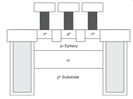
FIG. 29 Triple-well ESD device with p+ diffusion in an isolated p-well,
floating n-sub-collector, and deep trench (DT) isolation.
In a BiCMOS technology, S. S. Chen et al. used a sub-collector region and a deep trench (DT) sidewall to isolate the p-well region from the substrate to form a triple-well ESD diode string element. Using the sub-collector region and the DT sidewall isolation, the leakage current is reduced (e.g., compared to the singe- and dual-well series diode CMOS ESD power clamps) (FIG. 29). S. S. Chen showed that the Darlington leakage amplification effect can be significantly reduced. A first advantage of this triple-well ESD signal network is the elimination of the leakage amplification. A second advantage is the lack of parasitic interaction of adjacent elements due to the isolating sub-collector and DT structure. A third advantage is the ESD design layout density advantages. With the DT structure, the density between the successive stages are limited to DT spacings. Additionally, the usage of DT limits the out-diffusion of the sub-collector, providing a denser triple-well ESD power clamp design. A disadvantage of the DT-bound ESD power clamp is the use of a DT structure that increases the substrate thermal impedance. Hence, the power-to-failure will be impacted by the self-heating in the surface region. This can be reduced by using multiple-finger STI-defined p+ elements to widen the trench opening, reducing the impact of the trench structure.
Using a bias network, a new triple-well ESD power clamp can be formed. The bias network can electrically connect to the n-type isolating structure but is electrically disconnected from the diode string current path through the diode elements. Using a separate voltage biasing network, the triple-well isolation region can be connected to a separate voltage condition. W. L. Wu and M. D. Ker showed that using a bias network, a higher blocking voltage and lower leakage current can be achieved (e.g., compared to the case of a ''floating'' n-band triple-well structure). W. L. Wu and Ker also showed that a lower turn-on voltage is present when the n-band network is not electrically biased in the triple-well ESD power clamp structure. An advantage of this n-band-biased triple-well ESD power clamp is the reduction of the excess substrate current (compared to the floating n-band ESD power clamp+. A second advantage is that by separating the isolation region from the series diode elements, the successive diode stages can be physically merged, reducing design area. The design area between successive stages of the diode elements is limited to the width of the edge isolation region (e.g., n-well width) (FIG. 30).
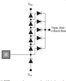
FIG. 30 Triple-well ESD power clamp network with independent n-band
voltage dc bias
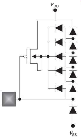
FIG. 31 Triple-well ESD network with n-band bias control network
In many applications, it is not desirable to have a power supply connected to the n-band network directly. It was also shown by W. L. Wu and M. D. Ker that it was not desirable to have the n-band region to float during circuit operation due to functional excess substrate current . Hence, a solution proposed by Voldman, Sloan, Pequignot and Stout is a triple well diode string where the first stage is electrically connected to a n-band bias network.
Using a p-channel MOSFET element, whose source is connected to VDD, whose drain is connected to its own p-channel MOSFET body, and whose gate is electrically connected to the input pad. The drain of the p-channel device is electrically connected to the n-band structure. When the input signal is below the power supply voltage, VDD, the p-channel MOSFET is in an ''on'' state, allowing biasing of the n-band structure. In this fashion, the n-band structure is biased at the VDD potential. When the input signal rises above the power supply, the n-band region floats. In this fashion, the n-band is suitable that is biased during functional operation (FIG. 31).
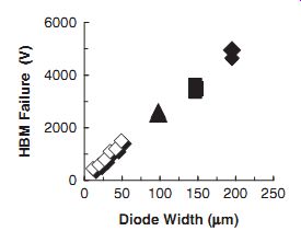
FIG. 32 HBM failure voltage as a function of diode width for an STI-bound
diode in an n-well with low-dose implanted sub-collector
9. ESD DESIGN: BICMOS ESD DESIGN
Mixing CMOS and bipolar structural elements, traditional STI-bound p+ /n-well diode structures and n-well-to-substrate diode structures can be modified by utilizing the sub collector implants, DT, and TI structures. Trench structures can provide reduced capacitance and physical isolation for RF performance, density, and latchup isolation.
Utilizing the sub-collector and reach-through implant in an n-well structure can provide a low-resistance cathode for a diode structure and prevent substrate hole injection. The enhanced recombination in the cathode of the diode structure also reduces the vertical pnp current gain. The physical design of these elements can be identical in nature to the CMOS STI-defined diode structures; in these cases, the sub-collector mask is placed under the n well, the DT and TI structures which border the n-well. In this fashion, the implementation is transparent to the p+ anode, n+ cathode, and metal design.
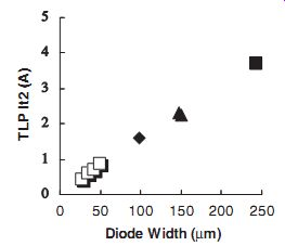
FIG. 33 TLP critical current as a function of diode width for STI-bound
p+ /n-well diodes with implanted sub-collector
9.1 p+/n-Well Diode ESD Structure with High Resistance Implanted Sub-Collector
Implanted sub-collectors provide an opportunity to scale the vertical profile of a BiCMOS SiGe HBT as well as lower manufacturing cost. In a technology with an implanted sub collector, the doping concentration is significantly lower than the pre-epitaxial sub-collector used in BiCMOS SiGe HBT devices. For the implanted sub-collector, the sheet resistance is on the order of 100 _ /sq. as opposed to the heavily doped sub-collector (e.g., approximately 10 _ /sq.).
HBM and TLP failure value of a STI-bound p+ /n-well diode structure with a low-dose implanted sub-collector (Figures 4.32 and 4.33). The TLP measurements are for single- and multi-finger structures. Single-finger structures were measured between 0 and 50 mm diode width. Multi-finger diode structures with a 0.72 _ 50-mm width for each finger were measured. HBM and TLP measurements do not show string roll-off effects. The following table summarizes the HBM, MM, and TLP results of a p+ /n-well diode structure with high-resistance sub-collector implant:
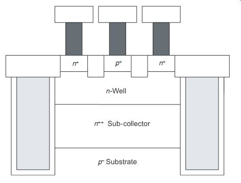
FIG. 34 Deep trench (DT) isolation and sub-collector defined STI-bound
P+ /n-well diode structure
9.2 STI-Bound p+/n-Well Diode with Deep Trench (DT) Isolation Structure
Table 2 HBM data of sub-collector-to-substrate diode with and without deep trench (DT) isolation
FIG. 34 shows the novel DT-defined collector STI-bound p+/well diode
structure.
The anode consists of an STI-bound p+ region and a n-well/STI-bound n+ cathode structure.
Mixing CMOS and bipolar structural elements, traditional STI-bound p+ /n-well diode
structures and n-well-to-substrate diode structures can be modified by utilizing the sub collector implants and DT. DT structures provide reduced capacitance and physical isolation for RF performance, density, and latchup robustness. DT extends below the n-well and sub collector junction eliminating the n-well/sub-collector sidewall capacitance. Utilizing the sub-collector and reach-through implant in an n-well structure can provide a low-resistance cathode for a diode structure, prevent hole injection, enhanced Auger recombination, and reduced vertical pnp current gain.
The presence of the DT structure increases the thermal resistance to the bulk substrate, leading to a higher temperature and earlier failure of the structure due to self-heating.
For negative ESD events, a DT-bound n-well and a non-DT bound n-well show a very significant difference; ESD results show non-DT bound structure, where HBM ESD results are 2_ the DT-bound structure (Table 2). The advantage of the DT-bound structure is a lower capacitance ESD element, density, and constraint of electron injection into the substrate.
9.3 STI-Bound p+/n-Well Diode With Trench Isolation (TI) Structure
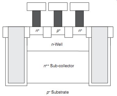
FIG. 35 TI-bound p+ /n-well diode structure. The TI structure extends
to the implanted sub collector depth.
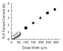
FIG. 36 TLP measurements of a TI-bound multi-finger BiCMOS p+ /n-well
diode (with implanted sub-collector)
A second type of trench structure is called trench isolation (TI) [31]. This technology utilizes an implanted sub-collector. The implanted sub-collector is significantly shallower than epitaxial-based buried sub-collector. The implanted sub-collector dose and energy are reduced to avoid high capacitance at the base-collector metallurgical junction. With the shallower collector structure, the depth of the adjacent isolation is not as deep as those used in the DT implementations (FIG. 35). This has an advantage for cost and performance. In this structure, the TI is formed after shallow trench isolation (STI) and all front-end-of-line processing. The isolation structure extends along the sidewall of the collector region For ESD, latchup, and substrate injection, the TI structure has considerable advantages over non-trench structures. The TI prevents lateral diffusion of the sub-collector toward the p-well edge or adjacent n+ diffusions or sub-collector structures. Hence, lateral parasitic effects are greatly reduced. This lowers the electric field in reverse bias and the isolation breakdown voltages. Second, it prevents lateral current injection minimizing lateral substrate injection and latchup concerns. From an ESD design implementation perspective, this allows the placement of an ESD structure closer to other structures without the concern of parasitic interaction.
For a p+ /n-well diode input node ESD network, this structure will allow for a low capacitance sub-collector-to-substrate metallurgical junction ESD element. The TI-bound cathode and STI-bound anode p+ /n-well diode structure will provide a very low capacitance diode structure.
A BiCMOS SiGe technology p+ /n-well with the low doped sub-collector implant and trench sidewall was designed with variable length and multi-fingers. HBM, MM, and TLP measurements show good ESD linearity within a single finger and in multiple fingers with no clear roll-off implications. TLP measurements of the p+ /n-well structure exceeded the 4.5 A TLP tester limit for structures larger than 300 mm total width (FIG. 36).
10. SUMMARY AND CLOSING COMMENTS
In this Section, the ESD layout, design, and operation of diodes, and diode string ESD networks were discussed. The diode elements discussed were fundamental elements used in CMOS, RF CMOS, and BiCMOS technology. Although the focus was on single-well and dual-well CMOS, the concepts can be extended to triple-well CMOS, triple well BiCMOS, and silicon-on-insulator (SOI) technology.
In Section 5, the design and layout of SOI elements are discussed. The Section will discuss the design of SOI MOSFETs, SOI polysilicon diodes (e.g., Lubistor), and SOI buried resistor elements. The understanding of design and layout of SOI elements is important for the design of ESD elements, receiver networks, and peripheral OCD networks. With the ability to compare bulk CMOS and SOI networks, a better understanding of both bulk CMOS, triple-well CMOS and SOI is achievable.
PROBLEMS
1. Assuming a diode string ESD network of N successive stages of area A1, A2, and AN, derive a general relationship so that the current is uniform through all successive stages.
2. Assuming a first diode string with N diode elements and bipolar current gain _1, and diode area A1, and a second diode string of M diode elements and bipolar current gain
_2, and diode area A2, derive the general relationship so that the turn-on voltage is equal. Solve for the area A2.
3. Assuming a first diode string with N diode elements and bipolar current gain _1, and diode area A1, and a second diode string of M diode elements and bipolar current gain
_2, and diode area A2, derive the general relationship so that the on-resistance is equal. Solve for the area A2.
4. Given a circular diode with an annulus first ring of the p+ diffusion of inner radius R1, and outer radius R2, and a second annulus for the n)-well contact of inner radius R3 and outer radius of R4, calculate the diode series resistance. Assume an n-well sheet resistance of _. Assume that the inner region is not utilized (e.g., inside the inner radius of the p+ diffusion anode). Given a rectangular p-n diode structure with the same n-well sheet resistance, what is the width of the rectangular diode to achieve the same diode series resistance? (Note: Assume that the isolation spacing equal to the difference between R3 and R2).
5. Given a circular diode with a first circle of the p+ diffusion of radius R1, and a first annulus for the n)-well contact of inner radius R2 and outer radius of R3, calculate the diode series resistance. Assume an n-well sheet resistance of _. Given a rectangular p-n diode structure with the same n-well sheet resistance, what is the width of the rectangular diode to achieve the same diode series resistance? (Note: Assume that the isolation spacing equal to the difference between R1 and R2).
6. In the above cases, given the linear rectangular diode has the same length as the outer p+ anode diode edge, assuming the linear diode has a different n-well, solve for the sheet resistance of the linear diode which would achieve the same diode series resistance.
7. Solve for the resistance expression derived from the Worley and Bakulin ladder network model where
8. From the Worley-Bakulin derivation of the R-G ladder network, normalize the resistance expression to the expression to the case of a zero-ohm wire resistance, as well as express as a function of Rp and
9. Derive the Worley-Bakulin R-G diode ladder network assuming the current through the diode network is flowing in and out on the same physical end (e.g., anti-parallel current flow).
10. Derive the normalized expression as a function of the zero-resistance wiring case, and as a function of the two parameters.
11. Derive the ratio of the resistances for the parallel and anti-parallel wiring cases.
Prev. | Next