AMAZON multi-meters discounts AMAZON oscilloscope discounts
1. OFF-CHIP DRIVERS (OCD)
Electrostatic discharge (ESD) design of a transmitter circuit, also known as OCD, is a fundamental piece of providing ESD protection for a semiconductor chip design. In system environments, OCD networks transmit the signals between semiconductor chips as well as from the semiconductor system to outside of the system. These semiconductor chips can have different power supply voltages, different technology generations, and different technology types; in this environment, it involves both mixed-signal and mixed-voltage interface conditions. Additionally, standards are established for signal transmission to allow standardization of the signal levels being transmitted between logic, memory, analog, and other support circuitry. At the same time, there are also application requirements. These requirements can include the following concepts:
_ Power supply-to-power supply sequence independence.
_ Input pin-to-power rail sequence independence.
_ ''Power boundary'' conditions.
_ Cold sparing requirements.
_ Fail safe requirements.
_ ''Hot socket'' or ''hot plug'' requirements.
The first concept of power supply-to-power supply sequence independence is the requirement that there are not sequencing conditions on the states and rates of the different power supply within a given chip or system; the second condition is the same condition that applies between the signal pins and any power supply rail. The third condition, ''power boundary constraints'' is a general concept of power flow in or out of any section of a system when certain elements are in powered or unpowered states. Cold sparing is a concept that some segments of a system are powered or unpowered, and the system must not use power to the unused or unpowered sections of a system; this language is used in redundant and power managed segments of a system (e.g., redundant segments of a space application, micro processor, or even the voltage island concept). The concept of ''fail safe'' is similar-the capability to ''fail'' without detriment to other devices that remain powered. A fail safe OCD prevents failure when a receiver is not connected, whereas the unconnected receiver shows no detriment to the system. Hot plugging is the ability to remove or insert a chip or board into a system without having to power up or power down a chip, board, or system without destruction to signal integrity or system failure. As a result, a large plethora of OCD circuits exist, which satisfy these applications, and a large number of ESD design issues and ESD circuit topologies are associated with these OCD network conditions.
1.1 Off Chip Drivers I/O Standards and ESD
In peripheral I/O design, different logic levels exist for the different power supply voltages for receiving or transmitting signals. These logic levels will be a function of the transmitted power supply voltage, and the receiving power supply voltage of the two system components.
TTL standard was valuable for 5.0 V peripheral I/O interfaces. The TTL standard took advantage of bipolar transistors as well as CMOS technology. The TTL standard uses large current levels to drive logical ''1'' above the 3.5 V level, as well as logical ''0'' below 1 V levels. A characteristic of TTL signals is that the inputs to a gate rise toward a logical ''1'' if unconnected; this requirement for driving a TTL input is to ''pull-down'' the level to near 0 V. The current levels used for TTL drivers are typically of a milliamperes (mA) level for a given input; this results in significant power consumption and limited speed for fast applications. The response time of TTL gates is on the order of tens of nanoseconds (ns).
As a result, applications are limited to clock speeds of 50 -100 MHz.
From an ESD perspective, the response of TTL networks is on the same time scale as ESD phenomena. The speed of TTL networks are on the order of the rise time of the HBM impulse, but slower than the rise time of machine model (MM) and charged device model (CDM) events.
As MOSFET transistors were scaled, the power supply voltage level decreased. With the lowering of the power supply voltage and the need for faster data rates, new logic standards are established. Some of the voltage standards established are as follows:
_ LVTTL.
_ GTL.
_ HSTL.
_ SSTL .
TTL, LVTTL, GTL, HSTL, and SSTL logic levels will require different circuit topologies in order to receive and transmit signal. As a result of these logic level standards for transmission or receiving, the mixing of levels will lead to new circuit innovations and new ESD requirements. As the standard voltage levels decrease (e.g., the expected data rates increase), the requirement on the ESD protection strategy will be modified. As the logic standard performance increases, the desire to have a lower capacitance ESD network will be more significant; this will influence the ESD input device type and size, the power bussing, and the type of ESD power clamp and its placement requirements. As the I/O evolution transitions take place from 100 MHz TTL applications to 1-10 GHz applications, new ESD scaling requirements will occur. Additionally, as the speed of the I/O becomes faster, the circuitry will be more responsive to the ESD events (e.g., HBM, MM, and CDM). This will inevitably change the nature of how the devices, the circuits, and the semiconductor chip react to the ESD events.
1.2 OCD: ESD Design Basics
ESD design of OCD networks, independent of the circuit or structure, have some fundamental design concepts and objectives:
_ Buffering: Provide an ESD design strategy that buffers the OCD network and have an independent ESD network discharge the ESD current.
_ Current sharing: Provide an ESD design strategy that utilizes the OCD to assist in the ESD current discharge additional to the ESD network.
_ Ballasting: Provide an ESD design strategy that utilizes the OCD network, and uses resistor ballasting to distribute the ESD current through the network to maximize the ESD efficiency in the discharging structure.
_ Self-protection: An ESD strategy that uses the OCD network as the ESD protection network with no additional elements.
A first ESD strategy is to provide ESD protection in OCD networks by preventing the flow of current into the network. This can be achieved by using resistive elements. Resistors can buffer the OCD network to avoid avalanche breakdown and second breakdown. Whether MOSFET or bipolar OCD networks, using series resistor elements can achieve this objective.
A second ESD strategy is to allow the OCD to participate in discharging the ESD current.
This ESD design practice can be implemented in such a fashion to utilize the area of the OCD as well as the ESD element.
A third ESD strategy is to allow the OCD to participate in the discharging the ESD current, but maximize the current distribution within the OCD network. In this fashion, this prevents failure of the OCD network, and yet allows the ability of the OCD to discharge the ESD current.
In a fourth ESD design practice, the OCD network provides the ESD protection. In this fashion, no additional area is used for the ESD network, and the physical OCD network is optimized for performance and ESD objectives.
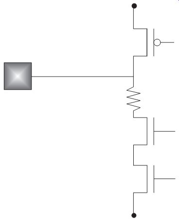
FIG. 1 Asymmetric pull-up/pull-down CMOS OCD with pull-down resistor
ballasting
1.3 OCD: CMOS Asymmetric Pull-Up/Pull-Down
In CMOS OCD networks, p-channel MOSFET devices are used as pull-up elements, and n-channel MOSFETs are used as pull-down elements [37]. In a CMOS OCD network, the n-channel MOSFETs are sensitive to positive-polarity ESD events. n-channel MOSFET pull-down elements undergo MOSFET snapback followed by MOSFET second breakdown during HBM, MM, and TLP ESD events, leading to OCD failure. p-channel MOSFETs pull up elements do not undergo MOSFET snapback or MOSFET second breakdown during positive-polarity ESD events. As a result, the n-channel MOSFET pull-down of an OCD is typically the cause of ESD failure.
To protect the n-channel MOSFET pull-down stage, resistor elements are placed in series to prevent MOSFET snapback and MOSFET second breakdown (FIG. 1). These can be integrated as a single resistor or a set of ballast resistor elements. The ballast resistor elements can be either configured as a bank of resistors or integrated with the n-channel MOSFET source and drain regions.
In the case of the p-channel MOSFET pull-up element, no resistor elements are used for ESD protection. With the use of a resistor element in series with the n-channel MOSFET pull-down without a resistor element in series with the p-channel element, the MOSFET driver has an asymmetric switching condition; this can be an undesirable characteristic for the OCD transitions.
From an ESD perspective, the lack of a resistor element in series with the p-channel MOSFET pull-up element can lead to an improvement in the ESD robustness of the OCD network. In the p-channel MOSFET pull-up element, the p-channel MOSFET drain and the n-well region form a parasitic p-n diode between the input pad and the power supply. During a positive polarity ESD event, this parasitic element serves as a means to discharge current from the input pad to the power supply rail.
The effectiveness of the use of the p-channel MOSFET pull-up to provide ESD protection is a function of the p-channel MOSFET design layout and the n-well contact design. By the placement of n-well contacts regions adjacent to the p-channel MOSFET pull-up drain regions, the series resistance formed between the p-channel MOSFET drain and the n-well contact can be minimized. The effectiveness of the structure is a function of the MOSFET width (e.g., diode perimeter), the p-channel MOSFET drain to n-well contact spacing, and the n-well sheet resistance of the technology. The optimum design is achieved by placement of n-well contact regions between the p-channel MOSFET drains in a multi-finger p-channel MOSFET pull-up element.
In this fashion, the MOSFET pull-up element serves as a p+/n-well diode element between the input pad and the power supply voltage. Given there is an p+/n-well ESD diode between the input pad and the power supply voltage, both the ESD diode and the p-channel MOSFET will be in a parallel configuration. Given there is no additional ESD element, the p-channel MOSFET pull-up will serve as an ESD element, providing protection for the asymmetric OCD network. Experimental results in semiconductor chips have demonstrated over 10-kV HBM protection levels without failure in 0.35-mm technology in a self-protecting asymmetric driver, which utilized a resistor-ballasted n-channel MOSFET pull-down, and an n-well contact integrated p-channel MOSFET pull-up with no additional ESD device.
The placement of n-well contacts can also be integrated between p-channel MOSFET pull-up stages where the p-channel MOSFET is multiple stages for improved slew rate control. In this case, the n-well contacts can be placed between the different stages of the MOSFET pull-up. In this case, the n-well contacts were placed between the successive stages of the MOSFET pull-up. Receiver networks with an ESD double-diode element, but without the OCD, demonstrated 4.2-kV HBM levels. The addition of an asymmetric OCD network (e.g., single resistor in series with the n-channel MOSFET pull-down, and no resistor element in series with the p-channel MOSFET) demonstrated 9.4-kV HBM.
The integration of the n-well contacts with the p-channel pull-up stage improved the HBM ESD results because of the parallel operation of the ESD p+/n-well diode element, and the p-channel MOSFET parasitic p+/n-well diode.
The key ESD design practices for asymmetric OCD networks are as follows:
_ Resistor ballasts of the n-channel MOSFET pull-down, utilizing a single resistor, a resistor bank, a or integrated resistor element.
_ Utilize the p-channel MOSFET drain to n-well parasitic diode by integration of the n-well contacts between the p-channel MOSFET fingers.
_ Minimize the p-channel MOSFET parasitic p-n diode by maximizing the p-channel MOSFET width, and decrease the MOSFET drain-to-contact space.
1.4 OCD: CMOS Symmetric Pull-Up/Pull-Down
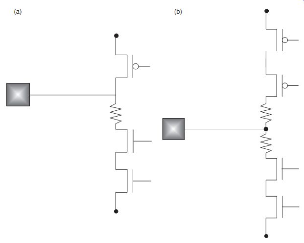
FIG. 2 (a) CMOS symmetric pull-up/pull-down OCD with pull-down only
ballasting; (b) CMOS symmetric pull-up/pull-down OCD with resistor ballasting
For switching symmetry in OCD networks, resistors are used in series with the p-channel MOSFET pull-up and the n-channel MOSFET pull-down. In a CMOS OCD network, the n-channel MOSFETs are sensitive to positive-polarity ESD events. n-channel MOSFET pull-down elements undergo MOSFET snapback followed by MOSFET second breakdown during HBM, MM, and TLP ESD events, leading to OCD failure. p-channel MOSFETs pull-up elements do not undergo MOSFET snapback or MOSFET second breakdown during positive-polarity ESD events. As a result, the n-channel MOSFET pull-down of an OCD is typically the cause of ESD failure. But, for negative-polarity ESD events, the p-channel MOSFET can undergo MOSFET avalanche breakdown, but without a negative resistance transition. ESD failure of p-channel MOSFET devices can be observed in negative-polarity ESD events. Additionally, CDM failures can also be evident between the p-channel MOSFET pull-up n-well and the p-channel MOSFET drain. Although these have been observed, it is fairly uncommon in most applications.
The placement of a resistor element in series with the p-channel MOSFET pull-up will impact the effectiveness of the p-channel MOSFET pull-up in improving the ESD robustness of an OCD. Whereas, the OCD may have achieved better switching symmetry, the ESD results may degrade. One significant result of the series resistor is that the OCD will no longer serve as a self-protecting structure, and will require an ESD network (e.g., ESD double-diode element). Additionally, the p-channel MOSFET pull-up will no longer assist in the positive polarity ESD event. To compensate for the ESD robustness degradation, a larger ESD element will be required to provide ESD protection for the symmetric OCD.
FIG. 2 (a) is a circuit schematic of a symmetric series-cascode MOSFET p- and n-channel MOSFET with resistor ballasting only in series with the n-channel pull-down.
FIG. 2 (b) is a circuit schematic of a symmetric series-cascode MOSFET p- and n channel MOSFET with resistor ballasting for both pull-up and pull-down components.
The key ESD design practices for a symmetric OCD networks are as follows:
_ Resistor ballasts of the n-channel MOSFET pull-down utilizing a single resistor, a resistor bank, or a integrated resistor element.
_ Resistor ballasts of the p-channel MOSFET pull-up, utilizing a single resistor, a resistor bank, or a integrated resistor element.
_ With the ballasting of the p-channel MOSFET pull-up, the utilization of the interwoven n well contacts may provide no additional ESD advantage.
1.5 OCD: Gunning Transceiver Logic (GTL)
GTL was established by B. Gunning to address a low power standard that allows for low electromagnetic interference at high data rates [1,2]. This is achieved by using a small signal swing to differentiate between a logical ''0'' and logical ''1.'' The GTL signal swings between 0.4 and 1.2 V with a reference voltage of about 0.8 V; a small deviation of 0.4 V from the reference voltage is required. The low terminating voltage of 1.2 V leads to reduced voltage drops across the resistive elements. GTL has low power dissipation and operates at high frequency. The GTL scheme is established by having the transmission line termination at the far end; in this fashion, it is similar to an ''open'' drain.
In the GTL OCD implementation, a low-resistance, active ''pull-down'' element is required. This is typically achieved using a low-resistance single large n-channel MOSFET device. In many implementations, a resistor termination is used as a ''pull-up'' element. The logic levels swing does not undergo ''rail-to-rail'' transitions but limited about a given dc current level. In some implementations of GTL, an n-channel MOSFET ''pull-up'' is used in the OCD network; this element mimics a resistive load for a ''pull-up'' transition.
In the ''open drain'' or a GTL OCD, the p-channel MOSFET is not mandatory. In this case, there is no physical element in the OCD to provide protection from positive-polarity human body model (HBM) events and the positive-polarity swing of a machine model (MM) event. Additionally, since a low logic level as well as a low-resistance MOSFET pull-down, is required, a single n-channel MOSFET is only used; as a result, the GTL OCD will undergo MOSFET snapback during positive-polarity ESD events.
In some implementations of a GTL OCD, the network contains both an n-channel MOSFET pull-up and an n-channel MOSFET pull-down element. In this implementation, there are some unique ESD differences compared to a standard CMOS OCD network:
_ An n-channel MOSFET exists between the input and VDD.
_ An n-channel MOSFET exists between the input and VSS.
_ A series-cascode MOSFET is formed by the GTL network between the VDD and VSS at all input pins.
The interesting feature of this architecture from an ESD perspective is that in a positive polarity pulse, the n-channel MOSFET will undergo MOSFET snapback relative to the VDD and the VSS power supply [17]. Second, as it discharge to a given power rail, the other parallel pins create a series-cascode MOSFET pair, serving as ''pseudo-ESD power clamps'' along the chip. The other pins will limit the level of the power rail to the sum of the MOSFET snapback voltages of the pull-up and the pull-down element.
ESD protection can be achieved using the following ESD solutions:
_ Low-resistance double-diode networks.
_ MOSFET devices.
_ Low-voltage trigger Silicon controlled rectifier (LVTSCR) ESD elements.
1.6 OCD: High Speed Transceiver Logic (HSTL)
HSTL is a logic standard established for voltage-scalable and technology-independent I/O circuitry. HSTL nominal switching range is from 0 to 1.5 V; this allows for faster I/O response, lower power consumption, and lower sensitivity to electromagnetic interference (EMI). HSTL does not specify the power supply voltage, but is established around a reference voltage condition; this leads to a technology-independent standard. As a result, the HSTL standard is free from the technology generation (which is constrained by MOSFET constant electric field scaling law, dielectric thickness, and power supply condition). The HSTL interface standard is one of the only logic level standards for a single-ended interface at higher speeds; LVTTL, GTL, and SSTL can not achieve the same performance levels.
HSTL uses an adjustable voltage reference trip point (VREF) and an output voltage (VCCO).
Four classes of HSTL interfaces exist; these are a function of the load and termination conditions. The HSTL standard is valuable for memory applications, such as high-speed static-rams (SRAMs), which require both the noise immunity, low power, small signal swing, and high performance. Since the memory applications are typically at a lower power supply than the control processor unit (CPU), it is a natural solution and I/O standard.
In HSTL I/O, matching of the I/O circuit with the termination and load conditions is important.
In the HSTL I/O standard, the ESD protection networks must conform to the impedance matching conditions between the I/O network, the termination and load to avoid transmission line reflections, ringing, and sensitivity to EMIs. Traditional ESD solutions, such as series resistor elements and resistor-ballasted MOSFET networks, interfere with the impedance matching, signal swing, and output drive levels. Additionally, resistor-ballasting elements and resistors do not improve the signal drive but increase the power consumption within the I/O.
In SRAM application, an interface was constructed that has the ability to comply with both the HSTL and GTL standards. In this chip application, two I/O drivers were integrated into a common signal pin. In this implementation, there was a pull-up stage of two parallel n-channel MOSFET elements and a pull-up stage of two parallel elements, consisting of a p-channel and an n-channel MOSFET. In the application, the I/O was able to undergo transition from HSTL to GTL mode, by initiating the pre-drive of the corresponding I/O network.
From an ESD perspective, the integration of both HSTL and GTL standards into a common I/O has some ESD design advantages:
_ Increases the effective size of I/O network.
_ Provides both a p-channel and n-channel MOSFET pull-up.
_ Increases the size of the n-channel pull-down network.
As previously discussed in the GTL application, the integration of a n-channel MOFSET pull-up allows for MOSFET snapback between the input and the power supply voltage when the power supply voltage is the ground reference. When the substrate is the ground reference, MOSFET snapback will occur in the two parallel MOSFET pull-down network elements. Additionally, the p-channel MOSFET will discharge current to the I/O power supply rail; and the n-channel pull-up MOSFET element in the adjacent pins will allow for current flow to the ground reference, when the voltage between I/O power rail and the ground exceeds the sum of the MOSFET snapback voltage of the n-channel MOSFET pull up and pull-down elements.
For ESD protection solutions, the following are possible for this application:
_ Diode-based ESD elements.
_ Poly-bounded diode ESD elements.
_ LVTSCRs
6.1.7 OCD: Stub Series Terminated Logic (SSTL)
SSTL standard was developed to support high-band width DRAM applications. SSTL standards have been developed for a wide range of power supply voltages from 3.3 to 1.8 V. SSTL standards have a 3.3, 2.5, and 1.8 V centered power supply level. SSTL3 and SSTL2 are general purpose 3.3 and 2.5 V memory bus standards, respectively. The standards require a push-pull OCD and differential amplifier input buffer, and have two general classes of application. SSTL_18 is a SSTL standard for the 1.8 V centered power supply levels.
SSTL3 and SSTL2 Class I and II are single-ended output buffers. SSTL OCD networks are typically a CMOS OCD with a single p-channel MOSFET pull-up and a single n-channel MOSFET pull-down. As the power supply voltage decreases, and as the performance objectives of the SSTL I/O increase, the ESD solutions have low voltage turn-on and low capacitance.
ESD solutions used for 1.8-V SSTL input have included the following:
_ ESD diode to VDD.
_ Low-voltage RC-triggered silicon controlled rectifier in series with diode string.
ESD solution used for 1.8-V SSTL OCD has included the following:
_ Low-voltage RC-triggered silicon controlled rectifier in series with diode string.
C. H. Chuang and M. D. Ker implemented an ESD input network that included a diode element to the power supply, and a LVTSCR element to the ground plane. In this implementation, the LVTSCR MOSFET gate was triggered by an RC-trigger network whose response was obtained from both the VDD power supply and the signal pad. The LVTSCR was also in series with a set of two diode elements to prevent early initiation during functional operation. Excellent HBM and MM results were demonstrated into the input circuitry even without power rail implementations.
Additionally, diode-based elements can achieve excellent ESD protection for the SSTL standard. Diode elements will not impact the signal levels, reflections, and transmission characteristics other than in the loading condition at the OCD end. The ESD choice must have a low resistance and must not impact the matching characteristics or the performance of the SSTL OCD network.
2. OFF-CHIP DRIVERS: MIXED-VOLTAGE INTERFACE
With MOSFET constant electric field scaling, density and performance objectives continue to scale MOSFETs to smaller physical dimensions. This leads to the lowering of power supply voltages within a system. Within a system or multi-chip environment, the scaling of all segments does not occur concurrently; for example, memory chips are typically designed in the scaled technology, whereas the logic chips are in a prior technology generation. With mixed-voltage applications, new OCD networks need to satisfy this condition.
Additionally, the introduction of multiple power supply voltage levels within a chip introduced complexity in the chip architecture, bussing, sequencing, and ESD protection schemes [17-21].
3. OFF-CHIP DRIVERS SELF-BIAS WELL OCD NETWORKS
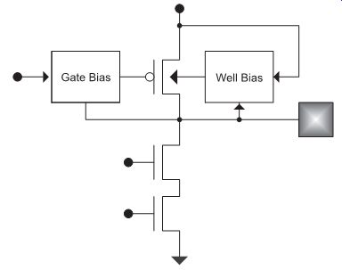
FIG. 3 Self-bias well OCD networks
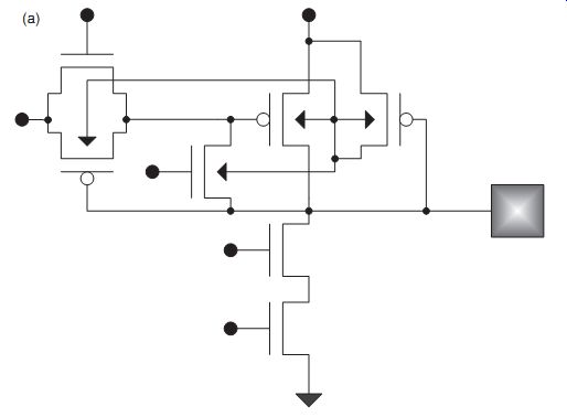
FIG. 4a Self-bias well OCD networks
MOSFET constant electric field scaling theory requires to maintain dielectric reliability, the power supply voltage must be scaled with the dielectric thickness. As a result, the high performance applications and semiconductor chips using advanced lithography tools will have the thinnest dielectric thicknesses and the lowest power supply voltages. In a system environment, mixed-voltage interface OCD networks are required to address the interaction between the older technologies at higher power supply voltages and the microprocessor and memory semiconductor chips at the lower power supply voltages.
Mixed-voltage interface off-chip drivers (MVI-OCDs) were first developed to address the transition from 5 to 3.3 V interfaces between logic and memory. R. Flaker, H. Kalter, K. Gray and R. D. Adams first addressed the MVI OCD with the introduction of the self-bias well network for the p-channel MOSFET. The pull-down network and pull-down networks consisted of two n-channel transistors and two p-channel transistors in a series cascode configuration, respectively. In the pull-down transistor network, the first n-channel MOSFET has its gate connected to the internal voltage power supply; this first n-channel MOSFET serves as a transmission gate that limits the voltage condition on the n-channel MOSFET pull-down element. The unique feature of the implementation was the self-bias well network; a p-channel transistor serves a control network that decouples the pull-up network well region from the power supply voltage of the low-voltage semiconductor chip.
As the input signal rises above the power supply voltage, the well-bias control network allows the well to undergo a floating state, preventing the pinning of the n-well to the VDD power supply voltage. The use of the n-well bias network provides a means of decoupling the input signal from the power supply rail.
This concept was extended to other self-bias well and mixed-voltage interface networks:
…. In these other implementations, additional transistor elements were added to provide improvements to provide electrical overstress protection of the p-channel MOSFET pull-up, improved n-well voltage level, and improved n-well voltage control.
Fig. 3 shows the basic architecture of a self-bias well. FIG. 4 (a) and (b) show examples of the implementation of Austin, Piro, and Stout implementation, and the …
Dobberpuhl implementation for a series-cascode self-bias well network respectively. These networks were initiated in a 0.5- and 0.35-mm technology generation.
From the ESD perspective, a first significant observation was the ESD robustness of the upper p-channel transistor with the auxiliary p-channel self-bias well elements that demonstrated HBM ESD robustness levels of 6-8 kV HBM. With the self-bias well pull-up element, the upper segment of the self-bias well driver demonstrated significantly high HBM ESD robustness due to the decoupling means and electrical overstress protection elements. A second observation noted that although the upper segment was ESD robust, the turn-on voltage was not adequate to provide protection for a non-ballasted n-channel pull-down network in the floating well segment. A third observation was that the ESD robustness did not scale with future technology generations. A fourth observation was that without the discharge means to the VDD power supply, the response was dependent on the lateral pnp response.
These OCD networks were interesting in that they contained circuit concepts, which were useful for ESD design, as follows:
_ Electrical decoupling of the n-well prevented electrical overstress of the p-channel element.
_ Electrical decoupling of the n-well prevented dielectric gate overstress.
_ Inherent robustness was exhibited using the lateral pnp of the p-channel element with a self-biased n-well.
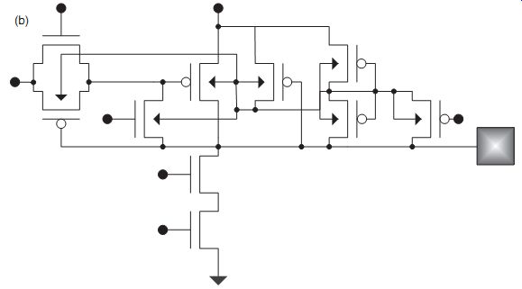
FIG. 4b Self-bias well OCD networks
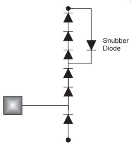
FIG. 5 Snubber-clamped diode string ESD network
3.1 OCD: Self-Bias Well OCD Networks
3.2 ESD Protection Networks for Self-Bias Well OCD Networks
In the mixed-voltage interface environment, the self-bias well OCD is utilized to allow the receiving of voltage levels above the native power supply voltage of the low-voltage semiconductor chip. ESD input protection solutions consist of three different solutions:
_ Snubber-clamped ESD diode string network.
_ ESD diode string with a second power supply pin added after the first diode.
_ Self-biased well ESD protection network.
The first implementation utilized a Snubber-clamped ESD diode string. As discussed in the prior section, this consisted of a five-diode string between input and the VDD power supply pad (FIG. 5). With the Snubber-diode element, the Darlington amplification was eliminated. But, in high bipolar current gain semiconductor processes, the vertical pnp effect leads to an I-V characteristic shift approximately 1V lower than the ideal characteristic; this leads to a sub-''turn-on'' leakage characteristic level, which is not acceptable near the higher temperature and voltage specification (this was demonstrated by G. Gerosa and S. Voldman in a microprocessor CPU with a retrograde well technology process). ESD HBM levels of 8 kV were achieved in this implementation.
A second ESD circuit used for mixed voltage applications was the self-bias well ESD protection network developed by S. Voldman; this ESD circuit incorporated the self-bias well concept of R. Flaker [10,11], and utilized a lateral pnp element for ESD current discharge. FIG. 6 (a) and (b) show the network circuit schematic and layout, respectively. This network achieved excellent results when utilized with a mixed-voltage interface self-bias well OCD network (this was demonstrated by Gerosa and Voldman in a second microprocessor CPU with a diffused well technology process). HBM ESD protection levels over 4 kV were achieved in this implementation.
A third ESD input strategy was to add a extra power pin to the lower voltage chip application; an extra power pin was added after the cathode of the first diode of the ESD diode string, and the rest of the diode elements were then between the first higher voltage power pin and the native power supply voltage. As a result, a Snubber-diode was not needed (this was incorporated by A. Correale and S. Voldman into an embedded controller architecture). ESD HBM levels of over 5 kV were achieved in this implementation.
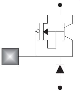
FIG. 6a Self-biased well ESD network schematic
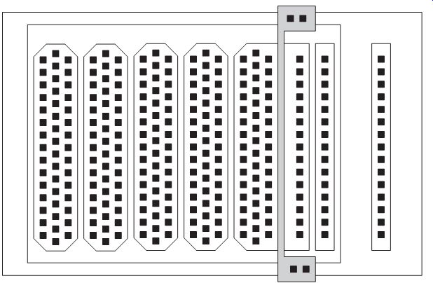
FIG. 6b Self-biased well ESD network layout
4. OFF-CHIP DRIVERS: PROGRAMMABLE IMPEDANCE (PIMP) OCD NETWORKS
PIMP OCD networks are used as a mean to match impedances with external loads.
To avoid ringing, an output OCD can be set with a given voltage level, drive strength, and impedance that matched the I/O device and transmission line. Low I/O drive strength need an OCD with a high impedance, and a high I/O drive strength will require a low-impedance OCD. Since the load can vary, it is desirable to have an OCD, which can be modified according to the required load needed to be driven. In semiconductor manufacturing, process variations also can lead to variation in the output impedance of an OCD element.
Additionally, power supply and temperature variations can modify the OCD impedance.
Hence an OCD, which can be self-tracking and provide matching with a transmission line and an external load, is important for many semiconductor chip and system applications.
T. J. Gabara and S. C. Knauer addressed the problem by providing an OCD network with a digitally adjustable resistor element. In this method, a variable resistor external to the OCD allowed for a fixed OCD design but addressed the impedance by providing a variable matching resistor element that was digitally adjustable. A user may change the external resistor of the driver to reflect the voltage/impedance, needed to drive an external load element. The OCD has an impedance that matches the transmission line; the OCD transistor width is adjusted by digital methods. In this concept of Gabara and Knauer, the overall impedance of the OCD circuit is obtained through the circuit's counter circuit networks that provide a digital ''count.'' Digital counter circuits are used to ''lock'' in that final count value. From an ESD perspective, as the resistor element increased in physical size, the OCD was buffered from the input pad, reducing the risk of ESD damage. In this implementation, the resistor element is modified.
In another method of providing a PIMP OCD network, the impedance of the OCD is modified using digital ''counters'' that modulate the size of the p- and n-channel MOSFET driven segments. By using the MOSFET OCD, the amount of power consumption, predictability, and accuracy is better obtained. H. Pilo, F. Towler, M. J. Schneiderwind, and S. Lamphier provided an output driver circuit that included the following:
_ An external impedance element.
_ Voltage comparator circuit.
_ Control logic circuit.
_ An evaluate circuit.
_ OCD output element.
FIG. 7 (a) shows the PIMP OCD network. Voltage from the ''external resistance device'' is compared with voltage created from an evaluate circuit by the voltage comparator; the control logic digitally adjusts the ''count'' until they are equated. After the ''counting'' process is complete by the control networks, the OCD MOSFET is increased or decreased in size to achieve the appropriate drive impedance.
In this implementation, there are unique ESD design issues, as follows:
_ Single MOSFET element: The pull-down n-channel MOSFET and pull-up MOSFET are not cascaded but single elements.
_ Series resistor elements: No resistor elements can be placed in front of the OCD MOSFET for ESD protection.
_ MOSFET design and layout: The MOSFET layout has a fixed channel length for all MOSFET finger segment but variable MOSFET finger width.
_ Ballasting elements: Resistor ballasting elements are not acceptable in the MOSFET fingers since they are matched with the adjustable counter network.
First, since only a single MOSFET element is utilized, MOSFET snapback voltage is a function of the channel length of a single MOSFET element. This provides a low turn-on voltage.
Second, since matching is required between the external load, the transmission line, and the internal MOSFET driver, no series resistance elements are acceptable. This prevents the buffering of the OCD MOSFET from ESD current.
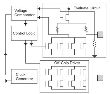
FIG. 7a PIMP driver network
Third, the width of the OCD MOSFET output device size is modified by adjusting the number of MOSFET fingers that are driven, which is established by the counting networks.
FIG. 7(b) shows an example of the programmable impedance driver MOSFET output device. In the physical layout, the width of the different fingers are of different widths for each finger grouping. This introduces an interesting issue: the asymmetry of the MOSFET fingers in the width leads to non-uniform bussing considerations and distribution issues during MOSFET snapback and MOSFET second breakdown. Experimental work by Pilo and Voldman showed that in this implementation, the smallest width fingers fail first, starting from the smallest width fingers, to the largest width fingers.
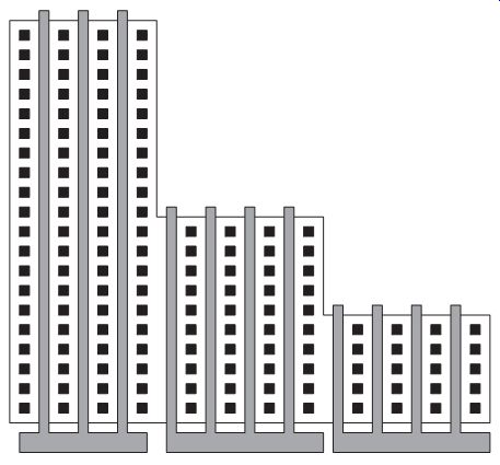
FIG. 7b MOSFET layout in a PIMP driver network
Fourth, the MOSFET finger elements must be of the same physical design as the adjustable counter structures. As a result, resistor-ballasting cannot be integrated into the MOSFET physical design of the output device unless ''mirrored'' in the adjustable counter network.
With these three issues, it is found that this is a difficult OCD to provide good ESD protection. Solutions for improvement are as follows:
_ Introduce ballasting elements in the adjustable counter network and the OCD elements with each finger element.
_ Utilize low-resistance ESD networks.
_ Utilize low-trigger voltage ESD power clamps.
Programmable impedance OCDs are important, as the need to efficient power transfer from driver to load and improved dI/dt control increases. Other circuit networks also exist that achieve the same objective. Hansen and Pilo developed another method using analog biases to provide the matching between the output and the load impedance; this was achieved using a digitally controlled current mirror network. PIMP OCDs will continue to provide challenges for ESD protection, as new implementation are developed.
4.1 OCD: Programmable Impedance (PIMP+ OCD Networks
4.2 ESD Input Protection Networks for PIMP OCDs
ESD input protection networks for PIMP circuits is limited as a result of the nature of this circuit. With the constraints of no series resistance element, a OCD final stage of a single MOSFET pull-down, and the minimum-channel length and variable width MOSFET layout, PIMP circuits, the ESD input protection network must have the following features:
_ An ESD trigger voltage below the minimum channel length MOSFET snapback voltage.
_ A low series resistance.
To provide ESD protection for this application, the most successful solution was achieved using very low-series resistance ESD double-diode networks on the input pad nodes and RC triggered MOSFET power clamps. Additionally, a low-resistance power bus was established using the stacking of multiple metal levels in the perimeter I/O design. In the perimeter I/O architecture, the metal bus resistance could compromise the ESD element and the RC triggered power clamp. As a result, wide metal busses and the use of multiple stacked metal lines were ''stitched'' to lower the bus resistance.
5. OFF-CHIP DRIVERS: UNIVERSAL OCDS
With the wide variety of logic levels of receiving and transmitting signal, the concept of a single receiver or OCD circuit that can interface without a new circuit but employs a suitable means of interfacing has significant advantages, where the system environment is either reconfigurable dynamically or for a wide range of applications. The desire has a ''universal interface''; that is, to establish a ''variable voltage CMOS OCD'' and receiver interface that can send and receive signals at different logic levels. Additionally, a second objective is to have a constant output impedance independent of the output voltage. This concept of a ''universal OCD'' would avoid the constant redesign of OCDs with each change in technology logic levels, as well as be able to interface with higher or lower power supply environments. P. Coteus, D. Dreps, G. Kopcsay, H. Bickford, C. Chang, and R. Dennard pursued the concept of the universal driver, where the different levels states were established using an integrated three-input multiplexor (MUX). In this fashion, the logic levels of receiving and transmitting were achievable with a single OCD circuit. To achieve a constant output impedance, different series resistance elements were used in series with the OCD output devices.
From an ESD perspective, the universal OCD produces a unique challenge as a result of the variable voltage levels. The universal OCD network must establish a constant impedance, and hence the resistor elements in the different segments of the network must be set by the different segment requirements. ESD protection can be established using the following circuit concepts:
_ ESD double-diode network.
_ Silicon controlled rectifier (SCR).
With the changing voltage levels, it is not possible to use a MOSFET ESD implementation, unless the MOSFET element exceeds the maximum MOSFET gate dielectric condition.
6. OFF-CHIP DRIVERS: GATE-ARRAY OCD DESIGN
6.1 Gate-Array OCD ESD Design Practices
In gate-array OCD environment, the design methodology and practices are distinct from a non-gate array environment. The gate-array design methodology provides opportunities and advantages for ESD design.
6.2 Gate-Array OCD Design: Usage of Unused Elements
ESD design practices can be implemented into gate-array OCD design to utilize segments of the OCD design book for ESD protection. In OCD design, MOSFET pull-up and pull-down stages are modified in drive strength by changing the elements, which are driven by the pre drive circuitry or modification of the gate connections.
An example, given a MOSFET pull-down network, where a fixed MOSFET width is contained within an OCD design book, the MOSFET gate connections can be modified so that segments of the MOSFETs are used for the OCD application. For example, given a MOSFET of width, W, where there are N MOSFET gate fingers, in a given application, only M fingers are used for the circuit application; this leaves N-M fingers unused in the OCD design book. In the network, the M gate fingers are electrically connected to the pre-drive circuitry, and the N-M MOSFET gate fingers are electrically disconnected from the pre-drive circuitry.
An ESD design practice in ESD OCD design is to utilize the unused portions of the MOSFET for ESD protection. A common ESD design practices are as follows:
_ Substrate grounding unused MOSFET elements: Electrically ground the N-M MOSFET gate fingers to the substrate.
_ Dummy pre-drive element for unused MOSFET elements: Electrically connect the N-M MOSFET gate fingers to a ''dummy circuit.''
_ Input gate-coupled network for unused MOSFET elements: A gate-coupled network is electrically connected to the input pad node to activate the unused segments of the MOSFET pull-down element.
In the first case, the unused MOSFET gate elements are electrically grounded (FIG. 8). In this fashion, as the input node voltage approaches the MOSFET snapback voltage, the unused portions of the MOSFET n-channel pull-down element serve as the ''grounded-gate MOSFET'' ESD protection elements. As the pad voltage rises, the MOSFET drain voltage increases, until the MOSFET undergoes MOSFET snapback. The N-M unused MOSFET gate structures begin to conduct current to the MOSFET source, discharging the ESD current. The MOSFET gate fingers driven by the OCD pre-driver network do not undergo MOSFET snapback at the same voltage level. As the voltage continues to increase, the MOSFET fingers connected to the pre-drive network will also undergo MOSFET snapback. Note in this implementations, the N-M fingers, which are grounded, will undergo snapback at a lower voltage. This has the disadvantage that the ''used'' portion of the MOSFET pull-down does not turn on at the same condition, making the ESD results a function of the number of fingers that are used or unused.
In a second case, the unused portions are coupled to the input pad. In this fashion, the unused portions can be triggered using the following methods:
_ Gate-coupling.
_ RC-coupling.
_ Gate- and body-coupling.
Using these methods, the unused portions are utilized for ESD protection and to provide the earliest turn-on possible, and not for addressing the size of the ''used'' segment.
This will be successful, given that a minimum number of fingers are defined (e.g., N-M fingers are above some design limit to guarantee the ''smallest'' number utilized for ESD protection).
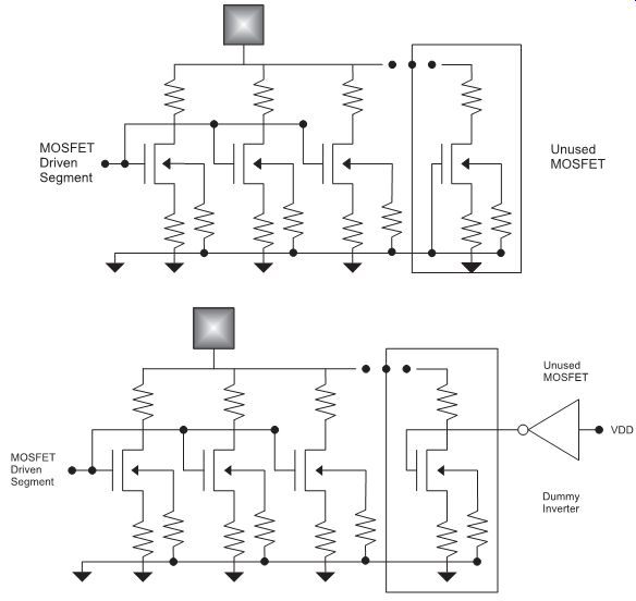
FIG. 8 (a) Gate-array MOSFET with grounded-gate unused fingers for ESD
protection (b) gate array MOSFET with unused fingers connected to dummy pre-drive
network
6.3 Gate Array OCD Design: Impedance Matching of Unused Elements
An ESD design practice in ESD OCD design is to utilize the unused portions of the MOSFET for ESD protection. Some ESD design practices are as follows:
_ Impedance match the used and unused MOSFET elements: Electrically connect the N-M MOSFET gate fingers to a dummy circuit that mimics the impedance of the ''used'' portions of the MOSFET.
_ Dummy pre-drive element for unused MOSFET elements: Electrically connect the N-M MOSFET gate fingers to a ''dummy circuit.'' A method that allows for an improvement is to provide impedance matching of the MOSFET gate fingers of the used and unused segments of a multi-finger MOSFET structure in an OCD circuit. This can be done with a simple network or a more complex network that mimics the pre-driver network.
In this ESD design practice, the unused MOSFET gates are not grounded but electrically connected to an auxiliary circuit or a ''dummy pre-drive network.'' In the prior discussion, it was noted that the driven and the undriven segments of the MOSFET pull-down have different electrical drain-to-gate voltage conditions, leading to different MOSFET snapback conditions. A dummy ''pre-drive'' network can mimic the impedance condition on the undriven N-M MOSFET gate segments (FIG. 8(b)). This can be done by using the following:
_ A dummy inverter network is connected to the unused MOSFET gate segments. The input of the receiver inverter is set at ''1'' to set the unused MOSFET gate segments to a ''0'' state.
_ A dummy pre-drive network sets the unused portions into a ''tri-state'' mode.
In this method, the objective is to have the impedance state of the used and the unused MOSFETs to undergo MOSFET snapback at the same voltage level, utilizing the full N
fingers concurrently; whereas in the first method, the ESD results will vary according to the number of unused versus used MOSFET fingers; this methodology aims at fully utilizing all elements at the same time, making it also gate-array implementation-independent.
6.4 OCD ESD Design: Power Rails Over Multi-Finger MOSFETs
The placement of the power rails and electrical connections influences the ESD robustness of a multi-finger MOSFET due to thermal heating of the inter-connect and inter-level dielectric (ILD) insulators. In a single pull-down or cascoded series MOSFET structure, the current flows from the pad to the VSS ground rail. The ESD current that flows to the VSS ground rail is then redistributed through the VSS ground network or to the local VSS pad.
Experimental results showed that when the multi-finger MOSFET pull-down is electrically connected to a VSS ground rail that exists on a second metal level (M2), the MOSFET second breakdown occurs under the VSS metal bus. As the current flows from the MOSFET to the local VSS bus connections, the heating of the metal and the surrounding insulating regions influences the underlying MOSFET structure. The failure of the MOSFET fingers occurs directly under the metal bus as opposed to the location anticipated by voltage distribution of a parallel- or anti-parallel configured multi-finger MOSFET.
The influence of the local heating is a function of the ESD pulse width and current magnitude, the vertical spacing of the metal bus to the MOSFET silicon surface, the type of the ILD material, and the interconnect metallurgy. The local self-heating within the metal bus is a function of the metal width, as well as the metal via connections. In the design, the local heating can be evaluated. The ESD design practices to avoid this issue are as follows:
_ Avoid passing the power and ground bus directly over the multi-finger MOSFET pull down network, where the power bus or ground is within one to two metal levels of the MOSFET metal connections.
_ Use a large number of metal vias and adequate metal bus width to distribute the current from the MOSFET to the power rail.
7. OFF-CHIP DRIVERS: GATE-MODULATED NETWORKS
7.1 OCD Gate-Modulated MOSFET ESD Network
An important ESD concept in ESD networks is the role of the gate potential during ESD events. D. Krakauer, K. Mistry, and H. Partovi in the analysis of operation of a MOSFET ESD protection network discovered some unusual response of the OCD network and the ESD devices. Using a simple grounded-gate MOSFET network to protect an OCD network, it was found that the ESD current that discharges to the I/O power rail initiated the pre-drive circuitry attached to the pre-drive network (e.g., the output stage and the OCD pre drive were connected to the external power supply voltage). The initiation of ESD current flow to the pre-drive network increased the gate voltage on the output drive stage; this in turn led to turn-on of the MOSFET pull-down transistor prior to the turn-on of the grounded-gate MOSFET ESD element. Krakauer, Mistry, and Partovi utilized this concept (as shown in FIG. 9 (a,b)) to develop a ''gate-modulated ESD network'' consisting of the following:
_ A discharge MOSFET whose drain is connected to the pad, and whose source is grounded.
_ An inverter network whose p-channel MOSFET source is connected to the input signal pad, and whose inverter output is connected to the discharge MOSFET gate.
_ An ''ESD reference'' signal pad that establishes a logic state for the inverter network.
_ An n-channel limiter MOSFET whose gate is connected to a resistor element, and whose drain is connected to the discharge MOSFET gate.
_ A resistor connected between the signal pad and the gate-voltage limiter element.
The important ESD design concept in this network is the following:
_ ESD discharge current can activate the pre-drive circuitry of an OCD if the pre-drive is connected to the external I/O power rail.
_ Gate modulation of the OCD pull-down can play a role in the ''current sharing'' with a parallel MOSFET-based ESD element.
_ The OCD pull-down can introduce ''current robbing'' during an ESD event if the MOSFET pull-down gate voltage state, coupling, or impedance to the ground plane is favored over the MOSFET ESD element.
_ Utilizing gate-modulation networks, a ''gate-coupled'' ESD MOSFET can provide a good ESD protection.
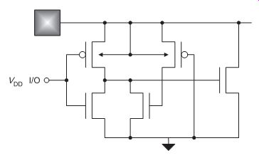
FIG. 9 (a) Gate modulated OCD network
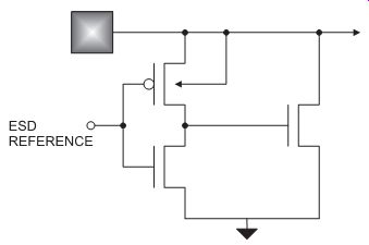
FIG. 9 (b) simplified gate modulated OCD network
7.2 OCD Simplified Gate-Modulated Network
From the prior implementation, Krakauer, Mistry, and H. Partovi utilized this concept (as shown in FIG. 9 (b)) to develop a ''simplified gate-modulated ESD network'' consisting of the following:
_ A discharge MOSFET whose drain is connected to the pad, and whose source is grounded.
_ An inverter network whose p-channel MOSFET source is connected to the input signal pad, and whose inverter output is connected to the discharge MOSFET gate.
_ An ''ESD reference'' signal pad that establishes a logic state for the inverter network.
The advantage of this ESD design concept is the ability to match with the technology generation, and the ability to simulate and model the circuit responses. The disadvantage of this ESD methodology is that it must be tuned for each I/O, each design, and each technology generation.
8. OFF-CHIP DRIVER ESD DESIGN: INTEGRATION OF COUPLING AND BALLASTING TECHNIQUES
A fundamental ESD concept in OCD networks is that to provide good current uniformity in a multi-finger MOSFET structure. With utilizing ballasting, coupling, and biasing techniques, the MOSFET second breakdown voltage, Vt2, can exceeds the MOSFET first breakdown voltage, Vt1, leading to MOSFET current uniformity in a multi-finger OCD network.
Multi-finger MOSFET ESD design utilizes both coupling and ballasting concepts to improve the current uniformity during high-current events in the OCD networks. Coupling and ballasting techniques can be integrated together to provide improved ESD robustness in MOSFETs. Some of the implementation can be utilized for OCDs but others are only suitable for ''unused gate array'' MOSFET segments, which are undriven by the pre-drive circuitry. The following implementations can be used for ''unused MOSFET gate array'':
_ Substrate grounded-gate (with gate resistor) resistor-ballasted multi-finger MOSFET.
_ Substrate grounded-gate (with gate resistor and capacitor element) resistor-ballasted multi-finger MOSFET.
_ Soft substrate grounded-gate resistor-ballasted multi-finger MOSFET.
_ Domino source-to-gate coupled resistor-ballasted multi-finger MOSFET.
The following OCD ESD design methodologies can be used in OCD and driven by the pre-drive circuitry:
_ MOSFET source-initiated gate-bootstrapped resistor-ballasted multi-finger MOSFET with MOSFET.
_ MOSFET source-initiated gate-bootstrapped resistor-ballasted multi-finger MOSFET with diode.
8.1 Ballasting and Coupling
8.2 MOSFET Source-Initiated Gate-Bootstrapped Resistor Ballasted Multi-Finger MOSFET With Diode
MOSFET source-initiated gate coupling can be implemented in a fashion, where one MOSFET source initiates a common MOSFET gate electrode. Utilizing a MOSFET source with two series resistor ballast elements and a center tap, MOSFET gate coupling can be initiated through a diode element. In the case that a MOSFET bootstrap element is used, this bootstrap element requires additional space as well as impacting capacitance loading on the signal pad. With the utilization of a diode element between the MOSFET source and the MOSFET gate electrode, no additional loading capacitance occurs on the signal pad, and less area can be utilized. In this network, the first conducting MOSFET finger source senses the ESD event, leading to a rise in the MOSFET source potential.
This first MOSFET finger source rises. The electrical potential of the MOSFET source resistor divider leads to an increase in the anode of the bootstrap p-n diode element. The bootstrap p-n diode element charges the MOSFET gate electrode when the p-n diode element becomes forward active. When the MOSFET gate electrode rises, MOSFET channel conduction occurs in all MOSFET finger elements providing uniform current flow. The advantages of this method allow for electrical connection of the MOSFET gate to a pre-driver network for utilization in OCD networks or in other circuits. This method also prevents the additional loading on the signal node compared to other bootstrap methods. A disadvantage of this method is that the diode elements must charge the complete MOSFET gate electrode. As a result, this method may be limited by the diode current drive, and the number of MOSFET fingers that can be driven by the bootstrap element (FIG. 10).
FIG. 10 MOSFET source-initiated gate-bootstrapped resistor-ballasted
multi-finger MOSFET with diode Bootstrap element
8.3 MOSFET Source-Initiated Gate-Bootstrapped Resistor Ballasted Multi-Finger MOSFET With MOSFET
FIG. 11 MOSFET source-initiated gate-bootstrapped resistor-ballasted
multi-finger MOSFET with MOSFET
MOSFET source-initiated gate coupling can be initiated to individual MOSFET fingers sequentially or all MOSFET fingers simultaneously. In an domino style implementation, the MOSFET fingers are gate-coupled in a sequential manner (FIG. 11). In the soft-grounded gate MOSFET, all fingers are initiated simultaneously. In the case of the individual sequential coupling technique, the response of the individual gate structures will have a faster RC time response for each individual fingers. But the disadvantage is the electrical disconnection of the MOSFET gate structure for utilization as a MOSFET off-chip pull down. Hence, these other implementations may be only implemented in a ''gate-array'' OCD design environment. But in this implementation, it can be integrated into a MOSFET pull-down network of an OCD.
MOSFET source-initiated gate coupling can be implemented in a fashion, where one MOSFET source initiates a common MOSFET gate electrode; the MOSFET source is electrically connected to two series resistor elements. The center node of the two resistor elements is electrically connected to initiate MOSFET gate coupling element. With a common gate electrode, the MOSFET source connection cannot be electrically connected to the MOSFET gate. Hence, an additional bootstrap MOSFET is placed between the signal pad and the MOSFET gate electrode.
The bootstrap MOSFET drain is connected to the signal pad, and its source is connected to the primary MOSFET gate electrode. The MOSFET source resistor center-tap is electrically connected to the gate of the bootstrap MOSFET.
In this network, the first conducting MOSFET finger source senses the ESD event, leading to a rise in the MOSFET source potential. This first MOSFET finger source rises. The electrical potential of the MOSFET source resistor divider leads to an increase in the gate of the corresponding bootstrap MOSFET element. The bootstrap MOSFET undergoes MOSFET conduction when the MOSFET threshold voltage is exceeded. The bootstrap MOSFET element charges up the MOSFET gate electrode, leading to MOSFET conduction in the other adjacent MOSFET fingers, which were not undergoing MOSFET snapback. The advantages of this method allows for electrical connection of the primary MOSFET gate to a pre-driver network for utilization in OCD networks or other circuits. The disadvantage of this structure is the need for an additional resistor and MOSFET for every segmentation of finger elements. This adds extra capacitance loading and space impact.
8.4 Gate-Coupled Domino Resistor-Ballasted MOSFET
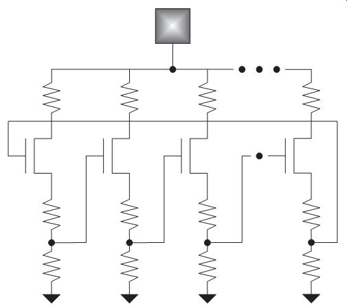
FIG. 12 Domino source-to-gate coupled resistor-ballasted multi-finger
MOSFET
As discussed on the Section on multi-finger MOSFETs, Mergens et al. introduced a ''domino'' method in a multi-finger MOSFET structure by electrically connecting the MOSFET gate of a second MOSFET finger to the MOSFET source of a first MOSFET finger (FIG. 12). In this domino source-to-gate coupled resistor-ballasted multi-finger MOSFET, the MOSFET source ballast resistor is split into a first and second resistor element. An electrical connection is established between the two resistor elements and electrically connected to the MOSFET gate of a second finger. This is initiated ad infinitum to all the finger elements. The ''nth finger'' MOSFET source connection is electrically connected to the MOSFET gate of the first MOSFET finger. In this fashion, the domino-triggering initiation can occur in any MOSFET finger in the structure. As the signal pad increases, the electrical potential of all the MOSFET drain structure increases. As the MOSFET drain potential increases, avalanche multiplication occurs. Eventually, one of the MOSFET fingers undergoes MOSFET snapback. As the electrical conduction occurs in the MOSFET finger, the current flows through the MOSFET source resistor elements. The two resistor elements form a voltage resistor divider. As the voltage increases, the MOSFET gate structure potential increases. As the MOSFET gate potential increases, adjacent MOSFET finger begins to conduct MOSFET source-to-drain current through the MOSFET channel region. As the second MOSFET finger conducts current through its own source, the electrical potential of the MOSFET gate of the third MOSFET finger increases. This continues in this fashion, until the ''nth'' MOSFET finger. As the ''nth'' MOSFET finger undergoes MOSFET conduction, the MOSFET gate of the first MOSFET finger that underwent MOSFET snapback will have its MOSFET gate potential increase, leading to MOSFET channel conduction instead of a MOSFET snapback state.
In this implementation, it was pointed out that the nature of the conduction and response in the ''Domino'' multi-finger MOSFET is different from other multi-finger MOSFETs, in the following ways:
_ The response of the network is current-driven (as opposed to frequency-driven).
_ The response is ''static'' phenomena not ''dynamic.''
_ The time response of the network is associated with the MOSFET gate delay time and the number of MOSFET finger stages.
_ The operation time is ''auto-timed'' and acts only during a fixed time interval, associated with the RC response of the successive stages, the MOSFET gate delay, and the number of successive stages.
In this implementation, the MOSFET current and the models are predictive models, as well as the circuit response. This implementation can also be integrated into a MOSFET gate array environment where the gate electrodes are separated from the pre-drive signal. As discussed in the prior section on gate array implementation, this network can be integrated into the unused MOSFET gate fingers of an OCD network.
9. OFF-CHIP DRIVER ESD DESIGN: SUBSTRATE-MODULATED RESISTOR-BALLASTED MOSFET
In a MOSFET OCD network, the injection phenomenon into the substrate can influence the MOSFET substrate potential and the MOSFET gate electrode. The local potential of the MOSFET structure can be modulated by injection phenomenon due to MOSFET drain.
Additionally, the MOSFET gate and substrate potential can be modulated by external source elements or circuits. As the potential locally increases under a MOSFET structure, a MOSFET reverse-body effect leads to a lower threshold voltage. The lower threshold voltage leads to an early turn-on of the MOSFET structure. This manifests itself in achieving MOSFET current uniformity in multi-finger structures, a lower turn-on voltage, and an increase in MOSFET current drive. C. Duvvury demonstrated different techniques to modulate the substrate and the gate electrodes via injection phenomenon or support circuitry.
ESD design practices to modulate the turn-on of OCD MOSFET networks can include the following:
_ Local substrate potential modulation separated from ''chip'' global substrate potential due to avalanche phenomena of the MOSFET OCD drain.
_ Local substrate potential electrical connections separated from the ''chip substrate'' using local guard ring structures connected to ''soft ground.''
_ Local substrate potential modulation using guard ring structures and external injection elements in avalanche breakdown (e.g., n+ diffusions).
_ Local substrate potential modulation using guard ring structures and external injection elements in forward bias (e.g., p-n diodes and p-channel MOSFET pull-up elements).
_ Local substrate potential modulation using guard ring structures and electrical substrate ''pump'' circuitry.
FIG. 13 shows an example where a p-n diode electrically connected to the MOSFET pull-down gate structure can electrically activate the MOSFET pull-down elements.
This ''diode'' element can be a defined element or parasitic diode element. This ESD design concept can be introduced in the unused sections of a MOSFET gate-array OCD network.
FIG. 14 shows a similar concept, where the p-channel MOSFET parasitic element is utilized for the gate coupling source. This can be an additional p-channel MOSFET or a parasitic element. FIG. 15 shows an example of a substrate pump network and a local substrate guard ring. C. Duvvury utilized an RC-network, which gate-couples the MOSFET structure. Additionally, a ''soft ground'' is connected to the local substrate regions. The ''soft-ground'' connections are also connected to the substrate through a ''substrate pump'' network that is initiated by the RC-trigger network.
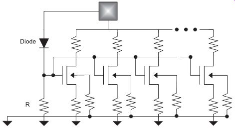
FIG. 13 p-n diode driven resistor-ballasted OCD MOSFET
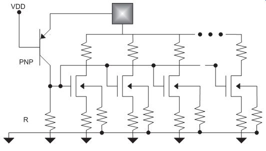
FIG. 14 p-channel
MOSFET driven resistor-ballasted OCD MOSFET
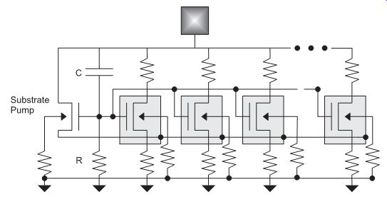
FIG. 15 Substrate-pumped OCD MOSFET
10. SUMMARY AND CLOSING COMMENTS
In this Section, we introduced both OCDs and ESD issues. MOSFET scaling, performance objectives, and new system environments changed a simple environment with simple circuits into an arena of different OCD circuit topology and issues; this also led to evolution of ESD circuits and solutions such as the Snubber-clamped diode string circuit, the self-bias well ESD circuit, and gate-modulated ESD circuit to multi-finger MOSFET domino concepts. A key point in the Section is that a number of circuit concepts from mixed-voltage environments have influenced the ESD concepts and vice versa.
In Section 7, the design and layout of CMOS and BiCMOS receiver networks are discussed. Receiver networks can be the most sensitive networks in a semiconductor chip in CMOS and RF CMOS applications. As the receiver networks evolve, the ESD solutions and issues vary. The Section will discuss the receiver evolution as well as the ESD solutions to provide better protection method for receivers. In this Section, it will be shown that OCD concepts and OCD ESD concepts are added to the ESD receiver solutions to provide better ESD receiver results. The understanding of receiver circuit topology and the parasitics is critical to achieving good ESD results in bulk CMOS, triple-well CMOS, and BiCMOS Silicon Germanium applications.
PROBLEMS
1. Given an OCD with a single p-channel MOSFET pull-up and a single n-channel MOSFET pull-down where the p-channel MOSFET width is twice the n-channel MOSFET width. Assume that between each p-channel MOSFET pull-up finger, there is a n-well contact strip connected to the VDD power supply. Show a representation of the p-channel MOSFET pull-up as a p-n ideal diode with a series resistor element.
Treat the n-well as a series resistor, whose width is equal to the width of the p-channel MOSFET pull-up, with a length equal to the p+ diffusion-to-n-well contact spacing, and a sheet resistance associated with the n-well. Assume all other resistances are negligible. Assume an ESD event occurs at the input signal pad of positive-polarity.
Derive the relationship of what the n-well sheet resistance and resistor element requirements to prevent MOSFET snapback to occur in the n-channel MOSFET pull-down.
2. Given the OCD in Problem 1, assume it is modified to two n-channel MOSFETs placed in series (in a series cascode configuration+ for MVI applications. Assume that the p-channel MOSFET pull-up width is double the single n-channel MOSFET pull down. Assume that the two n-channel MOSFET are of equal MOSFET channel length, and are not designed in a common p-well or common area. Assume that the MOSFET snapback is equal to the sum of the two MOSFET snapback values. Derive the relationship of what the resistor requirements are needed to prevent MOSFET snap back to occur in the series cascode MOSFET network.
3. Given the MVI OCD in Problem 2, assume that the two n-channel MOSFET pull down elements are integrated together into a common design layout. Assume that the MOSFET snapback is equal to Vtr1 ()cascode= _ Vtr1 () where _ is equal to a value between 1 and 2. Derive the relationship for the p-channel MOSFET resistance as a function of the integrated MOSFET pull-down network.
4. Assume that the relationship for the first trigger voltage in a mixed-voltage interface series cascode MOSFET is a function of the effective base width between the drain of a first MOSFET and the source of the second MOSFET. Show the relationship as a function of the MOSFET channel lengths and MOSFET gate-to-gate spacing. Can one relate the value of _ to the MOSFET channel length and gate-to-gate spacing ? How ? Note the relationship for _ is equal to
Vtr1 ()cascode= _ Vtr1 ()single
5. Given a dual function HSTL/GTL OCD network on a common input pad. The circuit contains a standard p-channel MOSFET pull-up and n-channel MOSFET pull-down.
Additionally, there is a n-channel MOSFET pull-up and n-channel MOSFET pull-down. The first network is driven by pre-drive circuitry independent of the second network. Show all the possible current paths between OCD signal pad, and the power rails VDD and VSS for positive and negative ESD pulses.
6. Given a dual function HSTL/GTL OCD network on a common input pad. The circuit contains a standard p-channel MOSFET pull-up and n-channel MOSFET pull-down.
Additionally, there is a n-channel MOSFET pull-up and n-channel MOSFET pull down. Assume the substrate rail VSS is grounded. Given a positive-polarity ESD pulse, the p-channel MOSFET pull-up discharges to the VDD power rail. In the case of all p-channel MOSFET pull-up networks, the current cannot discharge back to the ground rail through other parallel OCD circuits. In the case of the n-channel MOSFET pull up, current can return through the OCD itself or adjacent I/O or OCD circuits. Show the possible current paths making assumptions of the voltage potential on the power supply rail. At what voltage conditions do these occur ? What is the maximum power supply voltage during an ESD event?
7. Assume an off-chip driver uses a resistor element in series with a n-channel MOSFET pull-down, and a second resistor element in series with a p-channel MOSFET pull-up for OCD symmetry where the p-channel MOSFET width is double of the n-channel MOSFET width. As a result of the resistor in series with the p-channel MOSFET, a separate ESD p-n diode element is used to provide ESD protection. Calculate the percent extra area required as a function of the design variables of the OCD network to add the extra ESD network, given that the ESD p-n diode is equal to the p-channel MOSFET pull-up width (e.g., ratio of area for the ESD and OCD compared to the self protecting OCD network).
8. PIMP driver networks match the size of the MOSFET pull-up and pull-down elements as a function of an external resistor element. The external resistor initiates an adjustable counter that sizes the output impedance for the network. As a result, the MOSFET channel lengths are equal but the MOSFET finger widths are not equal but vary in physical size. Additionally, resistor-ballasting cannot be added. Where will the PIMP driver network fail? What is the solution to provide an ESD robust PIMP driver network?
9. In the mixed voltage interface networks, the p-channel MOSFET is used as an n-well bias network, first proposed by R. Flaker, where the p-channel MOSFET source is connected to the power supply, and its drain is connected to the n-well, and the p-channel MOSFET gate is electrically connected to the input pad. Experimental results show that this element never fails during HBM, MM, and TLP events. Why? Show the voltage conditions from the pad, the power supply, and the voltage stress conditions of the drain, source, and gate.
10. In the p-channel MOSFET pull-up stage of a ''floating well'' mixed voltage interface OCD, there are a number of p-channel elements to reduce the voltage stress, as well as establish the voltage potential of the p-channel MOSFET n-well. Show all the voltage conditions and operation purposes associated with the network. Can this network be used as an ESD protection network itself?
Prev. | Next