AMAZON multi-meters discounts AMAZON oscilloscope discounts
1. RECEIVERS AND ESD
Receiver circuits and the ESD protection of receiver circuits are very important in ESD design. Why? Almost all products and applications contain stand-alone receivers, or bidirectional receiver/transmitter circuits. Receiver circuits are typically the most sensitive circuits in a chip application. Receiver performance has a critical role in the semiconductor chip performance. First, receiver circuits are small. Second, the receiver performance requirements limit the ESD loading on the receiver. MOSFET gate area, bipolar emitter area, and electrical interconnect wiring widths impact the receiver performance. Third, receivers are electrically connected to either the MOSFET gate (in a CMOS receiver) or the bipolar base region (in a bipolar receiver); both the MOSFET gate dielectric region and the bipolar transistor base region are the more sensitive region of the structures. Hence, they evolve with MOSFET gate dielectric scaling and bipolar transistor performance objectives.
Fourth, receivers require low series resistance. Because of these factors, the receiver is also one of the most interesting network for evaluation of ESD protection. Since receivers are one of the smallest and most sensitive networks, it provides the opportunity to understand the future limitations on ESD protection of future technology generation, potential scaling implications, and lower limits of ESD protection levels achievable.
In this Section, we will discuss receiver, receiver evolution, ESD receiver problems, receiver ESD integration and solutions, as well as special classes of receiver networks.
Receivers with half- and full-transmission gates, zero-threshold voltage transmission gates, Schmitt triggers, and other networks will be used to discuss the issues and problems with receiver networks. The ESD protection sensitivity and solutions will be highlighted in the discussion.
1.1 Receivers and Receiver Delay Time
Receiver circuit performance can be quantified by the receiver delay time. A receiver response can be quantified as the intrinsic CMOS receiver gate delay, and the extrinsic receiver delay.
The CMOS intrinsic gate delay can be expressed as...
The extrinsic delay components of the receiver gate delay include the interconnect delay components of the CMOS gate delay and the ESD networks.
The interconnect delay components of the CMOS gate delay, excluding the intrinsic components, can be expressed as are the interconnect-related delay terms, Rd and Cd are MOSFET output resistance and capacitance (respectively), Cr is the MOSFET receiver switching capacitance, Rw, Cw, and Lw are the resistance, capacitance, and line length of the interconnect, and fg is the circuit fan-out. These interconnect delay terms become a larger percentage of the total CMOS gate delay as the intrinsic delay,
(Tg)int
= Rd(Cd ) fgCr), decreases and must be reduced through either interconnect resistance or capacitance reduction. Interconnect RC delay can be reduced by migrating from Al- to Cu-based interconnects, which improves electrical conductivity.
1.2 Receiver Performance and ESD Loading Effect
With the addition of ESD protection, receiver performance objectives must add the influence of the extrinsic loading on the receiver network. The extrinsic delay of the receiver can be represented as the extrinsic interconnect wiring load and the ESD element load.
An important ESD design consideration is the relationship of the extrinsic delay terms of the receiver network. As the receiver performance objectives increase, the total extrinsic delay of the receiver must be reduced. Hence, the loading of the interconnects, the ESD element, and any other auxiliary circuitry must be evaluated in the receiver performance. There are two issues. First, the scaling of the interconnects provides for the ability to have a larger percentage of the extrinsic delay term for ESD protection. Second, the scaling of the interconnect can lead to ESD failures. The transition from Al to Cu interconnects is important not only for semiconductor chip performance objectives but also for ESD robustness in high-performance chips. Aluminum interconnects was a significant ESD failure mechanism in high-pin-count microprocessor chips for the 250 nm and sub 250 nm technology generations due to the interconnect scaling and system level wire-ability requirements. With the migration to a low-k material, the extrinsic delay loading associated with interconnects can be reduced. As the interconnect extrinsic delay term is reduced, this will provide some reduced relief on the scaling of the ESD network extrinsic delay factor on receiver networks.
2. RECEIVERS AND ESD
Providing ESD protection for receiver networks is a challenge because of the receiver performance requirements and the receiver evolution for each technology generation [10]. A few standard circuit topologies are used for ESD protection of receivers for both HBM and CDM events.
2.1 Receivers and HBM
For HBM events, receiver networks used ESD networks include the following:
_ Primary stage of a grounded-gate thick oxide MOSFET, a resistor, and a grounded-gate thin oxide MOSFET element.
_ Primary stage of a double-diode ESD network.
In early development, grounded-gate ''thick oxide'' MOSFETs were designed using a parasitic device; the LOCOS isolation served as a thick oxide gate structure, and the LOCOS region defined the source and drain regions. The primary stage of the ESD network would initiate when MOSFET snapback occurred in the ''thick oxide'' MOSFET. Avalanche breakdown in the primary thick oxide MOSFET would allow conduction to the MOSFET source. Additionally, the standard MOSFET structure served as a secondary stage. With MOSFET avalanche breakdown in the thin oxide MOSFET, the secondary stage would provide conduction to the thin oxide MOSFET source. In conjunction with the resistor element, a resistive divider was formed, allowing a lower voltage on the input node of the MOSFET receiver gate dielectric. In some implementations, the substrate conduction lead to a dynamic threshold effect on the thick oxide MOSFET where the secondary stage influenced the primary stage triggering and conduction process. This topology was favored in NMOS technology where there was no p-channel MOSFET to utilize for ESD protection.
Additionally, with the introduction of shallow trench isolation (STI), the usage of the primary ''thick oxide'' MOSFET usage was curtailed because of the high turn-on voltage of the parasitic STI-defined npn element (FIG. 1).
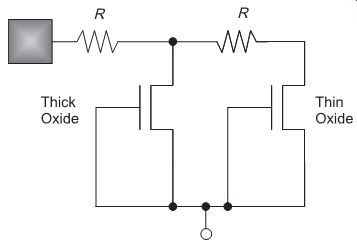
FIG. 1 Thick oxide/resistor/thin oxide MOSFET ESD network
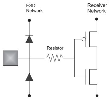
FIG. 2 Double-diode ESD network
Double-diode ESD networks using two diode elements between the input pad and the two power rails is used in CMOS technology. Diode structures were formed utilizing the p-channel and n-channel MOSFET source/drain regions as well as the well and tub regions (FIG. 2).
2.2 Receivers and CDM
For CDM events, receiver networks used ESD networks include the following:
_ Primary stage of a double-diode ESD network, a resistor, and a secondary stage consisting of a second double-diode ESD network.
_ Primary stage of a double-diode ESD network, a series resistor, and a secondary stage of a grounded-gate MOSFET ESD element.
FIG. 3 shows an example of an ESD network with a primary stage of a double-diode ESD network, a resistor, and a secondary stage consisting of a second double-diode ESD network. Some of the advantages of this network are as follows:
_ Scaling.
_ Migration.
_ Avoidance of dielectric regions.
FIG. 4 shows a second embodiment of a network that combines both the diode-based and MOSFET-based ESD protection. The advantage of this network is the utilization of the resistor/thin oxide MOSFET provides a resistor divider operation. This improves both the
HBM and the CDM ESD results. This CDM network has some of the following advantages:
_ Primary and secondary stages both active during HBM events.
_ Utilization of MOSFET drain for CDM protection.
_ Allowance of a lower series resistor element.
3. RECEIVERS AND RECEIVER EVOLUTION
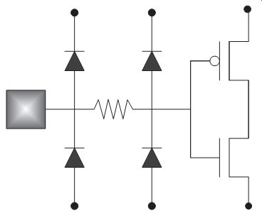
FIG. 3 Primary stage of a double-diode ESD network, a resistor, and
a secondary stage consisting of a second double-diode ESD network
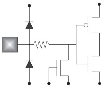
FIG. 4 Primary stage of a double-diode ESD network, a series resistor,
and a secondary stage of a grounded-gate MOSFET ESD element.
In CMOS, with MOSFET constant electric field scaling theory, the MOSFET dielectric thickness and power supply voltage are scaled to provide improved MOSFET device performance. With MOSFET dielectric scaling, power supply scaling, voltage signal level scaling, and the introduction of mixed-voltage interface applications, receiver architecture, and design continues to become more complex. In CMOS technology, for 5 and 3.3 V power supply, the dielectric thickness in receiver networks allowed for direct electrical connections to MOSFET gate structures. As the power supply was scaled, and with the introduction of mixed-voltage applications, the need to reduce the voltage stress on the dielectric was achieved using a transmission gate (TG) or pass transistor to lower the voltage levels. With decreasing voltage levels, mixed-voltage signals, and dielectric over-voltage condition concerns, a plethora of new receiver circuits evolved with new features: half-pass transmission gates, full-pass transmission gates, pseudo-zero threshold voltage transmission gates, zero threshold voltage threshold voltages, keeper feedback networks, and hysteresis feedback elements. Each of these provided new ESD receiver issues and challenges.
3.1 Receiver Circuits with Half-Pass Transmission Gate
A common element in a receiver network is a transmission gate network. A half pass transmission gate, using an n-channel MOSFET element is electrically connected between the ESD element and the MOSFET inverter stage of the receiver network. ATG has an influence on the ESD robustness of a receiver. The TG typically is involved in the ESD failure from HBM, MM, and CDM events. The TG structure is typically connected to the input pad, and the power supply, VDD, making it vulnerable during ESD events.
ATG is a voltage-controlled switch which has a high and low impedance state. In a half pass TG, the TG is typically a single MOSFET structure whose source and drain are connected in a series fashion between the input pad and the MOSFET receiver gate stage (FIG. 5). The MOSFET gate controls the logic state. When the n-channel MOSFET gate has a gate voltage equal to the power supply voltage, VDD, the logic transfers a logic ''1'' from the pad to the receiver.
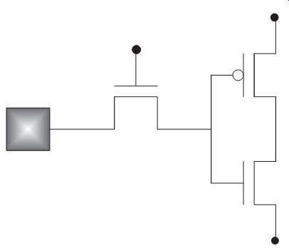
FIG. 5 MOSFET receiver network with n-channel MOSFET half-pass TG
Assuming the receiver network is initially uncharged, the output capacitance has an initial value. In this state, the voltage that will be observed at the output of the TG, assuming a loading capacitance, C, is [...]
...with a charging time of...
When the ratio of the time to charging time is long, the output voltage approaches the maximum output voltage, during functional operation of the circuit
Vout = VDD x VTn
From a functional perspective, the highest voltage output value is a threshold voltage lower than the voltage placed on the n-channel MOSFET gate electrode. The MOSFET half-pass transistor TG also has a characteristic resistance. The resistance can be expressed as
The resistance of the MOSFET half-pass transistor plays a role in the ESD event in that it current-limits the amount of current that can flow from the signal pad to the MOSFET receiver network. In conjunction with other circuit elements, and additional ESD elements, it serves as a resistor divider. During ESD events, after the MOSFET snapback voltage, the resistance of interest is the MOSFET dynamic on-resistance.
During ESD operation, there are two points that influence the operation of the n-channel MOSFET half-pass transistor. First, the output voltage will be dependent on the MOSFET gate voltage state. Second, the MOSFET snapback voltage has a role in the voltage drop, and the conduction process through the half-pass transistor.
In the case of the voltage on the MOSFET gate electrode, assuming the gate is floating, the state of the gate electrode is a function of the half-pass transistor input-to-gate capacitance and the other electrode capacitances that form a capacitor divider network.
As the input voltage increases, the capacitance coupling between the MOSFET half-pass transistor input-to-gate capacitor causes the MOSFET gate to rise.
At the same time, as the input voltage on the MOSFET pass-transistor increases, and the half-pass transistor drain-to-source voltage increases, the MOSFET snapback voltage is reached leading to MOSFET snapback. In order for MOSFET snapback to occur, the impedance in series with the MOSFET half-pass transistor must allow current conduction. In the case that there are no circuit elements except the MOSFET receiver inverter stage, the current conduction leads to a charging of the MOSFET gates. As the current flows through the half-pass transistor, the MOSFET gates of the inverter stage increases until the current through the MOSFET half-pass transistor fails, or MOSFET gate dielectric breakdown occurs.
In the case of additional other elements in the receiver network between the MOSFET half-pass transistor and the MOSFET receiver inverter stage, a current path can be established leading to current flowing through the MOSFET half-pass transistor, and the additional elements. The presence of the other elements can lead to MOSFET second breakdown of the MOSFET half-pass TG structure.
The introduction of the MOSFET half-pass transistor establishes a voltage margin allowing the operation of the ESD networks to discharge current away from the receiver network and through the ESD network current loop. For ESD events that occur at the input signal pads, the ESD elements should be placed between the signal pad and the MOSFET half-pass transistor (e.g., HBM, MM, and TLP events).
For charged device model (CDM) events, the ESD current flows from the substrate to the signal pad. In the case of a p- substrate which is charged positively, when the signal pad is placed at a ground potential, current will flow from the chip substrate to the signal pad.
When there is a n-channel MOSFET half-pass transistor TG, current will flow in a few different current paths.
_ First, current will flow from the substrate to the n-diffusion (e.g., p- substrate-to n-channel MOSFET diffusion metallurgical junction+ input side of the MOSFET half pass TG.
_ A second current path is through the MOSFET receiver inverter stage n-channel MOSFET gate and continued through the MOSFET half-pass transistor channel region (e.g., source-to-drain).
_ When there are more circuit elements present between the MOSFET half-pass transmission gate and the MOSFET inverter stage, current will flow through those circuit elements and through the n-channel MOSFET half-pass transmission gate.
In the case that the current is flowing from the output side of the MOSFET half-pass TG, there is a delay time that occurs to allow the current to flow to the signal pad from the interior of the chip. If we assume the MOSFET inverter stage, a capacitance, C, and the voltage rise to a maximum voltage condition, we can estimate the MOSFET half-pass transistor delay time by assuming the signal pad is at a ground potential [...]
...and discharge time [...]
During functional operation, the voltage V_ = VDD. During ESD events, the MOSFET half-pass TG voltage is a function of the capacitive divider formed between the gate-to source, and gate-to-drain capacitances.
From an ESD design perspective, the key issues associated with MOSFET half-pass transistor transmission gates are the following:
_ Half-pass MOSFET TG elements are to be placed between HBM ESD networks and MOSFET receiver inverter stages.
_ Half-pass MOSFET TG elements are vulnerable to ESD events due to the electrical placement in series with the MOSFET receiver inverter stage and the input signal pad.
_ Half-pass MOSFET TG element are vulnerable to ESD events due to the electrical placement in series with the signal pad and the power rails (e.g., VSS and VDD).
_ Half-pass MOSFET TG elements must be integrated with the HBM ESD networks, CDM networks, and additional receiver network functions to provide good ESD results in receiver signal pads.
_ MOSFET-based receiver network ESD failures typically involve failure of the MOSFET half-pass TG element.
_ MOSFET half-pass TG ESD failure during HBM events are typically MOSFET source to-drain failures.
_ MOSFET half-pass TG ESD failure during CDM events can be MOSFET substrate-to input diffusion contact and junction failure, MOSFET source-to-drain, and MOSFET gate-to-input diffusion failure mechanisms.
3.2 Receiver with Full-Pass Transmission Gate
A common element in a receiver network is a TG. TGs are in the form of full- and half pass TGs. A full-pass TG, uses a p-channel MOSFET and an n-channel MOSFET element.
The logic states of the full-pass transistor for the p-channel and n-channel half-pass elements are complementary. A TG is a voltage-controlled switch which has a high and low impedance state. In a full-pass TG, the TG has both the p-channel and n-channel MOSFET structure sources and drains connected in a series between the input pad and the MOSFET receiver gate stage . The MOSFET gate controls the logic state. When the n-channel MOSFET gate has a gate voltage equal to the power supply voltage VDD, the logic transfers a logic ''1'' from the pad to the receiver. When the p-channel MOSFET gate has a gate voltage equal to the power supply voltage VSS , the logic transfers a logic ''1'' from the pad to the receiver. FIG. 6 shows the full-pass TG electrically connected between the ESD element and the MOSFET inverter stage of the receiver network.
A full-pass TG has an influence on both the ESD robustness of a MOSFET receiver network. During a positive-polarity ESD HBM event, a positive pulse occurs on input pad. When the potential of the p+ /n-well diode element reaches forward bias, current flows through the diode element to the VDD power supply. As this occurs, the voltage potential on the input of the full-pass transistor begins to increase. In the case of an n-channel half-pass transistor, the voltage differential across the n-channel device would increase until MOSFET snapback would occur; if gate-coupling occurs, the half-pass may under MOSFET turn-on during ESD pulse events. In the case of the full-pass TG, as the voltage drop increases, the p-channel pass transistor p+ /n-well node will forward bias; this leads to forward-active operation of the lateral and/or vertical parasitic pnp bipolar transistor. In the case of the lateral parasitic pnp element, this will lead to a decrease in the voltage-differential across the full-pass TG. In some sense, the p-channel half-pass TG transistor prevents failure of the n-channel half-pass TG transistor. In the case of a negative-polarity event, the half-pass transistor will discharge to the semiconductor substrate, in parallel with the n-well= p-substrate diode ESD element.
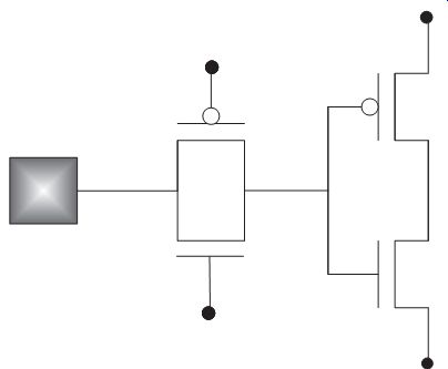
FIG. 6 Full-pass TG integrated between the ESD network and the MOSFET
receiver
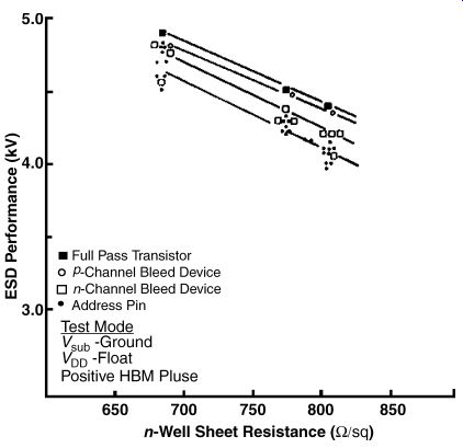
FIG. 7 ESD HBM results as a function of n-well sheet resistance of receiver
networks with and without full-pass transistor elements (with the grounded
reference VSS)
FIG. 7 shows the experimental results of a MOSFET receiver network as a function of n-well sheet resistance for a positive HBM pulse event (with the substrate grounded).
Experimental results show that the highest HBM ESD results occur with the full-pass transistor. FIG. 8 shows the experimental results of a MOSFET receiver network as a function of n-well sheet resistance for a positive HBM pulse event (with the VDD power rail grounded). A key point in the results is that the presence of the full-pass TG does not degrade the ESD protection results in the receiver. The experimental results show that the highest results occur with the presence of a p-type element on the input node, which improves the receiver network results. Independent of the n-well sheet resistance or reference polarity, for a positive pulse event, the highest address pin results occur with the full-pass TG.
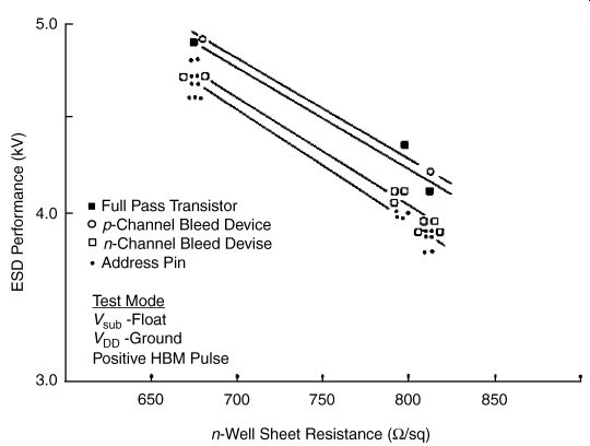
FIG. 8 ESD HBM results as a function of n-well sheet resistance of receiver
networks with and without full-pass transistor elements (with the grounded
reference VDD)
3.3 Receiver, Half-Pass Transmission Gate, and Keeper Network
With the introduction of the MOSFET half-pass TG in receiver networks, the quality of the CMOS logic levels is hampered in CMOS receiver networks. The half-pass TG, using an n-channel MOSFET element is electrically connected between the ESD element and the MOSFET inverter stage of the receiver network. A half-pass TG is a voltage-controlled switch which has a high and low impedance state. In a half-pass TG, the TG is typically a single n-channel MOSFET structure whose source and drain are connected in a series fashion between the input pad and the MOSFET receiver gate stage. The MOSFET gate controls the logic state. When the n-channel MOSFET gate has a gate voltage equal to the power supply voltage VDD, the logic transfers a logic ''1'' from the pad to the receiver.
The output voltage of the half-pass transistor can be expressed as [...]
...with a charging time of [...]
The output voltage then asymptotically approaches a maximum condition of...
When the power supply voltage of a technology is large compared to the MOSFET threshold voltage, the output voltage is within the receiver level to distinguish a logic ''1'' level from intermediate transition levels and logic ''0'' levels. The MOSFET threshold drop that incurs with a half-pass TG impacts the margin of a logic ''1'' level. The output level of the half pass transistor, which is below the full power supply voltage, is also referred to as a logic weak ''1'' state. When the weak ''1'' is present at the input of the MOSFET receiver inverter stage, the ability to have the MOSFET receiver inverter transition to a logic ''0'' is compromised. As technology is scaled, the power supply decreased from 5 to 2.5 V and the weak ''1'' logic level became a larger issue.
To address the impact of the half-pass MOSFET TG network on the receiver state, a ''half-latch,'' also known as a MOSFET keeper network, is placed on the output of the MOSFET inverter stage. FIG. 9 shows the MOSFET receiver network with the half-pass MOSFET TG and the MOSFET keeper network. In the network, a p-channel MOSFET keeper network source and drain is electrically connected to the input side of the MOSFET receiver inverter stage. The gate of the p-channel MOSFET keeper network is connected to the output stage of the MOSFET receiver inverter stage. In this fashion, the MOSFET keeper network serves as a feedback element between the output and the input of the MOSFET FIG. 9 MOSFET receiver network with the half-pass MOSFET TG and the MOSFET keeper network receiver inverter stage. Fundamentally, it is acting as a feedback latch, as is present in a latch network (e.g., this is present in latches, SRAM cells, and other applications).
In this network, when a logic ''1'' level is on the signal pad, the output of the MOSFET TG is a logic ''weak 1'' level. This is inverted by the MOSFET inverter stage to a weak logic ''0.'' The p-channel MOSFET keeper gate voltage is driven to a weak logic ''0'' state. When the p-channel MOSFET keeper voltage reaches the p-channel MOSFET keeper level, the keeper element conducts current between the VDD power supply and the MOSFET receiver inverter input stage. The p-channel MOSFET keeper charges the input of the MOSFET receiver inverter stage to the VDD power supply, leading to a good logic ''1'' state; this condition then outputs a good logic ''0'' state on the output of the MOSFET inverter stage.
The introduction of the p-channel MOSFET keeper network (e.g., half-latch feedback element), although it served significant value for logic functionality, introduces a new ESD failure mechanism in receiver networks. During an ESD event, where a positive polarity current pulse is applied to the signal pad, and the power supply VDD serves as a reference ground, the presence of the MOSFET half-latch circuit constrains the voltage potential of the half-pass MOSFET TG element. The reason is that the p-channel MOSFET n-well is electrically connected to a power supply VDD. When VDD is grounded, the metallurgical junction formed between the p-channel drain and the n-well region ''pins'' the electrical potential of the p-channel MOSFET keeper drain at the forward-bias diode voltage, Vbe. The parasitic diode formed between the n-well and the p-channel MOSFET keeper forces the half-pass MOSFET TG voltage to be constrained to within a forward bias voltage drop relative to the ground reference. In this fashion, the voltage from the signal pad minus the forward-bias diode voltage is there across the TG. During ESD testing, this leads to MOSFET second breakdown of the half-pass MOSFET TG. The physical damage is evident from the MOSFET source-to-drain junction, and within the p-channel MOSFET keeper drain (e.g., the p-channel MOSFET drain contacts to diffusion region). In the case that no p-channel MOSFET keeper is present, the output of the half-pass MOSFET TG rises until MOSFET gate dielectric breakdown of the MOSFET inverter stage. With the pinning of the half-pass MOSFET TG, the voltage-to-failure of the MOSFET receiver network is equal to the sum of the MOSFET second breakdown voltage, the forward-bias voltage of the p-channel MOSFET to n-well voltage, and corresponding series resistances in the n-well (FIG. 10).
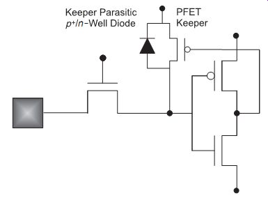
FIG. 10 MOSFET receiver network with the half-pass MOSFET TG and the
MOSFET keeper network, highlighting the parasitic diode electrically connected
to the VDD power supply voltage
The ESD degradation of the addition of the p-channel MOSFET keeper network was apparent in the evolution of the MOSFET receiver networks. In the evolutionary transition from 5 to 2.5 V power supplies with the CMOS scaling, these elements were introduced with a rapid decrease in the HBM ESD protection levels of receiver networks. J. Zimmerman and S. Voldman showed that in an integrated design with a signal pad, a diode-based ESD network, and a MOSFET receiver signal pad with a half-pass TG, an inverter, and a p-channel MOSFET keeper element lead the network achieved 2.5 kV HBM levels. It was shown that by removal of the p-channel MOSFET keeper element, the HBM ESD protection levels increased from 2.5 to 7.5 kV. This demonstrated that the impact of the protection levels were significantly impaired by the p-channel MOSFET keeper feedback element. An ESD design concept demonstrates that the presence of feedback element and the electrical connections of physical elements associated with the grounded references can impair ESD protection levels of receiver networks. The addition of small physical elements coupled to the power supply references can introduce significant reduction of protection results in some test modes.
To avoid ESD protection concerns with the MOSFET receiver network with the half-pass TG, inverter stage, and the MOSFET keeper feedback network, the following ESD design solutions can be implemented:
_ Add resistance in series with elements that do not impact circuit performance.
_ Eliminate the ''pinning'' of the output node of the half-pass TG.
_ Decouple the element from the grounded VDD reference.
To improve the ESD robustness of the receiver network, the following solutions can consist of the following:
_ Add resistance in series with the p-channel MOSFET keeper network between the MOSFET inverter stage input node and the p-channel MOSFET keeper drain node.
_ Add a resistor between the VDD and the n-well resistance of the p-channel MOSFET keeper network in series with the forward-bias metallurgical junction formed between the p-channel MOSFET drain and the n-well.
_ Add a resistor after the half-pass MOSFET TG node and before the p-channel MOSFET keeper drain node.
3.4 Receiver, Half-Pass Transmission Gate, and the Modified Keeper Network
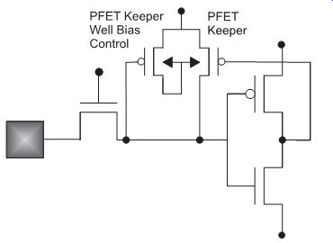
FIG. 11 MOSFET receiver network with half-pass MOSFET TG, an inverter
stage, and a modified MOSFET keeper half-latch network
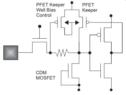
FIG. 12 Receiver network with the half-pass MOSFET TG, the modified
keeper network, and a charged device model (CDM) grounded-gate MOSFET
The introduction of the p-channel MOSFET keeper network (e.g., half-latch feedback element), although it served significant value for logic functionality, introduces a new ESD failure mechanism in receiver networks. During an ESD event, where a positive polarity current pulse is applied to the signal pad and the power supply VDD serves as a reference ground, the presence of the MOSFET half-latch circuit constrains the voltage potential of the half-pass MOSFET TG element. To avoid the ''pinning'' of the half-pass transistor MOSFET TG output voltage, the decoupling of the electrical node from the grounded reference power supply is needed. In the prior section, the means of decoupling recommended introduction of resistor elements in three different locations within the current path that initiates the ''pinning'' of the node by the p-channel MOSFET keeper network.
The electrical decoupling of the p-channel MOSFET keeper n-well node can be achieved by introduction of a network that allows the n-well to ''float'' when the VDD power supply is ground reference. FIG. 11 shows the introduction of a modified MOSFET keeper network. Voldman first introduced and applied the concept of the n-well bias control network to the half-pass MOSFET keeper network to avoid ESD concerns in receivers. The receiver network consists of a half-pass MOSFET TG followed by the MOSFET p-channel keeper element, and the MOSFET receiver inverter stage. An additional p-channel MOSFET is added whose source is electrically connected to the VDD power supply rail, and drain is connected to the n-well of the MOSFET p-channel keeper element. The p-channel MOSFET drain is also electrically connected to its own n-well. The gate of the new element is connected to output side of the half-pass MOSFET TG. Note that R. Flaker first introduced this concept for mixed voltage interface (MVI) off-chip driver (OCD) networks for decoupling of the p-channel MOSFET driver pull-up from the power supply. In this implementation, the concept of Flaker's ''n-well bias control network'' is applied to a receiver network feedback element and serves the ESD function to decouple the MOSFET feedback element node from the VDD power supply during ESD testing. In this implementation, there exist different networks to achieve the same objective.
In the operation of the network, when a positive polarity ESD pulse occurs on the signal pad, the input of the half-pass MOSFET TG begins to rise. Through capacitive coupling of the gate node, and the current flow through the half-pass transistor, the voltage increases on the output of the half-pass MOSFET transistor. As the half-pass transistor output rises, the first p-channel MOSFET gate rises, turning the p-channel MOSFET ''off.'' The p-channel MOSFET decouples the n-well node of the p-channel MOSFET keeper feedback element from the VDD power supply. In this fashion, as the voltage continues to increase, the metallurgical junction formed between the p-channel drain and the n-well region forward biases and charges up its local n-well, which ''floats'' but does not ''pin'' the voltage potential. The parasitic diode formed between the n-well and the p-channel MOSFET keeper no longer forces the half-pass MOSFET TG voltage to be constrained to within a forward bias voltage drop relative to the ground reference. With the modified keeper network, the output of the half-pass MOSFET TG rises until MOSFET gate dielectric breakdown of the MOSFET inverter stage.
As an ESD design practice, to avoid ESD protection concerns with the MOSFET receiver network with the half-pass TG, inverter stage, and the MOSFET keeper feedback network, the following ESD design solutions can be implemented:
_ Eliminate the ''pinning'' of the output node of the half-pass TG.
_ Decouple the element from the grounded VDD reference by introduction of logic circuitry.
_ Decouple the element from the grounded VDD reference by introduction of n-well or p-well bias control networks.
This network can be further extended by the introduction of charged device model (CDM) protection elements. A grounded-gate n-channel MOSFET can be added after the half-pass MOSFET TG network (FIG. 12).
4. RECEIVER CIRCUITS WITH PSEUDO-ZERO VT HALF-PASS TRANSMISSION GATES
With the introduction of the half-pass MOSFET TG, the threshold voltage impacts the quality of the logic level. One method to avoid the loss of the threshold drop is to provide a MOSFET with a zero threshold voltage (also known as a '' Zero VT'' MOSFET).
Another technique is to set the half-pass MOSFET TG voltage at a gate voltage so that the effective logic level is maintained.
In a standard half-pass MOSFET TG, the output voltage is equal to...
To establish a reference voltage, a voltage reference network can be constructed where the reference voltage is above the power supply voltage by the n-channel MOSFET half-pass TG threshold voltage.
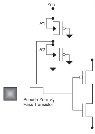
FIG. 13 Half-pass pseudo-zero VT TG
FIG. 13 shows an example of a voltage reference network for a half-pass pseudo-zero VT TG. M. Johnson utilized two p-channel MOSFET devices to form the gate reference voltage; two p-channel MOSFET transistors are used as a resistive voltage divider between a higher power supply rail and the ground rail. The gate of the p-channel transistors are established, so the MOSFETs are in a normally on-state during chip operation.
One issue with the receiver network is the potential of the electrical ''pinning'' of the half-pass transistor MOSFET gate electrode during ESD testing relative to the VCC and VSS power rails. When the VCC power rail is a grounded reference during ESD testing or events, the p-channel MOSFET of the reference network will pin the half-pass transistor MOSFET gate to within one forward-bias diode voltage. The metallurgical junction formed between the p-channel drain and the n-well will ''pin'' the half-pass transistor gate voltage. As the pad voltage rises, the half-pass MOSFET TG input-to-gate voltage will increase. This can lead to MOSFET dielectric breakdown in the input-to-gate region.
An ESD design practice can be instituted that prevents ESD failure as follows:
_ Add resistance in series with the half-pass transistor MOSFET gate electrode.
_ Add an isolating ''switch'' that decouples the half-pass transistor gate from the reference controller.
_ Decouple the voltage reference well nodes from the power supplies using n-well control bias networks.
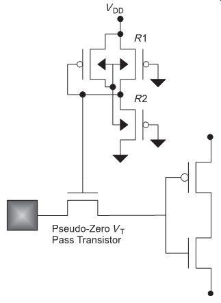
FIG. 14 Pseudo-zero VT half-pass voltage reference network with n-well
decoupling elements
FIG. 14 shows an example of a pseudo-Zero VT half-pass voltage reference network with n-well decoupling networks. As the half-pass transistor MOSFET TG input-to-gate voltage increases, the gate node rises. As the TG MOSFET gate electrode rises, the n-well of the voltage reference networks decouple from the VCC power supply electrodes. This allows the half-pass TG MOSFET gate electrode ''float'' and avoid electrical overstress.
5. RECEIVER WITH ZERO TRANSMISSION GATE
Receiver networks that utilize a TG (or pass transistor) have the issue of voltage level reduction at the output side of the TG when the threshold voltage is non-zero. Using a MOSFET with a zero threshold voltage (e.g., also referred to as a ''zero VT'' device), the threshold voltage drop across the TG in receiver networks can be avoided. Zero VT MOSFET devices are formed by constructing the MOSFET device as a standard MOSFET, but avoid the MOSFET threshold voltage implant and the p-well implant under the MOSFET gate structure. For example, a zero VT n-channel MOSFET is formed in the p-substrate wafer, or p- epitaxial region in a region without the p-well implant (FIG. 15).
The p-channel MOSFET threshold adjust implant is also blocked to avoid the increase in the MOSFET threshold voltage.
Zero VT devices are typically utilized in high-performance receiver applications.
Adams, Braceras, Connor, and Evans introduced a receiver network to achieve the following objectives:
_ Provide an input signal of the native voltage level to the gate dielectric (without the TG voltage drop).
_ Prevent overshoot voltage conditions that lead to dielectric over-voltage of the pass transistor or the MOSFET gate dielectric.
_ Prevent undershoot voltage conditions that lead to dielectric over-voltage of the pass transistor or the MOSFET gate dielectric.
_ Provide receiver which does not use multiple power supply voltages or burn dc power.
In the aforementioned circuit network, a zero-VT (ZVT) transistor is used as the pass transistor. Additionally, an n-channel MOSFET source is connected to the output of the TG transistor and its drain is connected to the MOSFET gate of the TG. The MOSFET gate of this element is electrically tied to ground. The gate of the MOSFET ZVT TG is not connected directly to the power supply, but is connected through an ''on'' p-channel MOSFET whose gate is grounded.
The MOSFET (ZVT) TG, also known as the ''ZPASS'' network prevents positive overshoot or mixed-voltage conditions to apply an over-voltage condition to the receiver gate structure. In this fashion, positive overshoots are limited to the voltage condition on the gate of the MOSFET (ZVT) device.
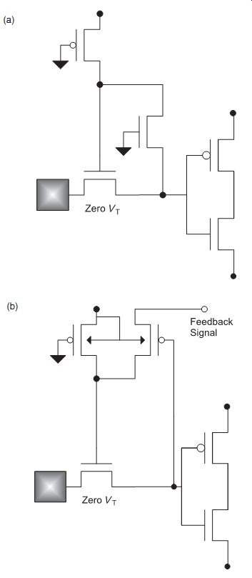
FIG. 15 (a,b) Receiver network with zero VT TG and dielectric over-voltage
network.
For a negative undershoot, current flows through the MOSFET (ZVT) TG, the n-channel transistor and the p-channel device. The p-channel and n-channel transistor serves as a resistor divider network whose center node voltage divides the condition on the MOSFET (ZVT) device gate structure. This prevents dielectric overstress of the TG dielectric, and also clamps the voltage condition on the MOSFET receiver gate dielectric.
Whereas this receiver network provides a good solution to minimize the overshoot and undershoot conditions on the MOSFET gate dielectric, the addition of the resistor-divider network introduces a current path for failure during ESD events. During ESD events, for the case that the power supply VDD is grounded, the MOSFET (ZVT) device, the n-channel, and p-channel elements provide a current path to the referenced VDD power supply. Experimental observations of the ESD testing results demonstrated MOSFET second breakdown of the ZVT, and the n-channel transistor, as well as damage in the p-channel MOSFET. Whereas the resistive-divider network served as a good solution to minimize electrical over-voltage during functional operation from mixed voltage interfaces, overshoot, and undershoot, the presence of the resistor-divider solution lead to the ''pinning'' of the output of the MOSFET ZVT transistor, leading to failure of the ZPASS network. ESD protection can be improved by good ESD protection prior to the ZPASS network, or additional resistance in the ZPASS resistor-divider network to prevent the ''pinning'' during ESD test conditions.
6. RECEIVER CIRCUITS WITH BLEED TRANSISTORS
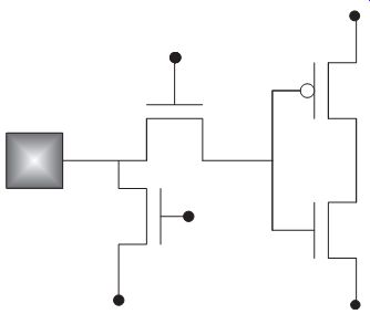
FIG. 16 Receiver network with n-channel bleed transistors
In receiver networks, noise and charge build-up on signal pads can initiate an undesired initial condition on an input pad or switching of the inverter circuit. To avoid charge build-up, half- and full-pass TGs are used to reduce the charge sensitivity. MOSFET transistors which are normally ''on'' can be used as resistors to maintain the low logic ''0'' state when no intentional signal is applied. Minimum-width long-channel transistors can provide a low width-to-length ratio suitable as a resistance element. Typical width-to-length ratios can be 1:50 and 1:100 providing very high resistance and low current drive. Receiver networks can use a narrow-width long-channel n-channel or p-channel MOSFET whose gate is either electrically connected to the input node or the power supply rails (Figures 16 and 17). In the case of the narrow-width long-channel p-channel MOSFET structure, the MOSFET gate is electrically connected to the ground potential to be normally ''on.'' In the case of the narrow-width long-channel n-channel MOSFET structure, the MOSFET gate is electrically connected to the power supply voltage to be normally ''on.'' In either case, the electrical connections of these normally ''on'' elements can lead to ESD failures which involve the gate-to-diffusion electrical overstress; these elements will not undergo MOSFET second breakdown due to the long channels. For example, given an narrow-width long channel n-type MOSFET whose gate is connected to the VDD power supply, electrical overstress can occur between the MOSFET drain and the gate region.
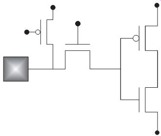
FIG. 17 Receiver with p-channel bleed transistors
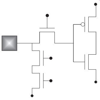
FIG. 18 Receiver
network with test functions
7. RECEIVER CIRCUITS WITH TEST FUNCTIONS
For functional testing, receiver networks are modified to allow the states of the receivers to be placed in various states. Test function are added by placing elements in a parallel with the signal path to avoid impacts to receiver performance. To avoid performance impacts, the elements are typically small, and hence vulnerable to ESD failure.
FIG. 18 is an example of a test function network that is placed on an input signal node of a receiver. Two MOSFETs are placed in a series cascode between the input signal and the VSS ground node. This network is placed in parallel to the half-pass MOSFET TG network. A first MOSFET has its gate electrically connected to the VDD power supply voltage. The second MOSFET gate is connected to test functions. The test function is the closest network to the signal pad. During CDM testing, a failure mechanism was evident between the first MOSFET gate electrode and the MOSFET drain. When the VDD is charged, and the input signal pad node is at a ground potential, the first MOSFET gate-to-drain overlap region leads to ESD failure.
In the ESD design of receiver networks, the following solutions can be applied to eliminate the failure of MOSFET test functions in receiver networks:
_ Test functions should be placed after the half-pass MOSFET TG to avoid both HBM and CDM failures.
_ Test functions connected to the power rails should introduce decoupling by placement of resistance elements in series with the MOSFET gate and source.
_ Test functions can place resistive elements in series with the MOSFET drain to avoid electrical overstress in receiver networks.
8. RECEIVER WITH SCHMITT TRIGGER FEEDBACK NETWORKS
Receiver networks can introduce feedback elements which provide higher tolerance to noise.
Schmitt trigger receiver networks introduce feedback elements to make receivers more tolerant to small input changes. A Schmitt trigger network introduces a hysteresis voltage where the forward and reverse voltage characteristics do not follow the same voltage transfer characteristic path. For the input characteristic, a higher input switching value is needed to switch the circuit when the input value is increasing. This state is referred to as a value of V). For the input characteristic, a lower input switching value is needed to switch the circuit when the input value is decreasing. This state is referred to as a value of V_. The difference between the two states is defined as the hysteresis voltage VH = V) ) V_ FIG. 19 shows an example of a receiver network with the Schmitt trigger feedback. In the receiver network, the p-channel MOSFET pull-up and the n-channel MOSFET pull-down elements are split into a series cascode MOSFET structure. Two elements provide the MOSFET feedback. In the case of an n-channel pull-down stage, an additional Schmitt trigger feedback n-channel MOSFET circuit element is placed; an n-channel MOSFET source is connected between the two n-channel pull-down MOSFETs and its drain is electrically connected to the local VDD power supply (e.g., or analog VDD). The gate of the Schmitt trigger feedback element is connected to the output of the MOSFET receiver output stage. In the case of a p-channel pull-up stage, an additional Schmitt trigger feedback p-channel MOSFET circuit element is placed; a p-channel MOSFET source is connected between the two p-channel pull-up MOSFETs and its drain is electrically connected to the local VSS power supply (e.g., or analog VSS). The gate of the p-channel Schmitt trigger feedback element is connected to the output of the MOSFET receiver output stage.
For the receiver network, the two switching conditions can be expressed as [...] where the first width-to-length ratio (W=L)n1 is the lowest receiver n-channel pull-down element, and the second width-to-length ratio (W=L)nf is the n-channel Schmitt trigger feedback element. The reverse trigger voltage is expressed as a function of the p-channel pull-up elements and the p-channel Schmitt trigger feedback element [...] where the first width-to-length ratio (W=L)p1 is the lowest receiver p-channel pull-up element, and the second width-to-length ratio (W=L)pf is the p-channel Schmitt trigger feedback element. A symmetric trigger voltage can be established using this receiver network where ...
...where the hysteresis is given by...
Given that the ratio of the MOSFET receiver stage to the Schmitt trigger feedback for the n-channel and the p-channel elements are the same, and assuming a threshold voltage for the n-channel and p-channel are equal in magnitude, it can be expressed as [...]
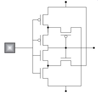
FIG. 19 Symmetric receiver network with Schmitt trigger feedback elements.
The MOSFET receiver network is vulnerable from ESD events due to the Schmitt trigger feedback element in the case where the ESD networks are connected to the VDD power rail.
Additionally, where this receiver network is placed on an independent power rail, such as analog VDD (e.g., AVDD). ESD failure of Schmitt trigger networks and erratic switching behavior on ESD test systems were first noted. During HBM testing, an ESD diode network can discharge the current to the AVDD power rail. As the ESD current flows to the AVDD power rail, the AVDD power rail voltage increases. As the voltage increases, MOSFET snapback occurs through the Schmitt trigger n-channel MOSFET feedback element and the n-channel MOSFET pull-down element. When the AVDD power rail voltage reaches the voltage condition where the Schmitt trigger and the pull-down MOSFET undergo MOSFET second breakdown, the circuit output failure occurs. From the tester, failure may not be observed since there is no rupture of the MOSFET receiver gate insulator, but the operation of the MOSFET receiver network will not have the same hysteresis character and switching points.
As an ESD practice, feedback elements can lead to early ESD failure of networks. An ESD design practice to prevent failure can be as follows:
_ Buffering of feedback elements: Buffer the feedback elements with series resistance to delay the turn-on.
_ Decoupling of feedback elements: Decouple feedback elements from the power rails.
_ Alternate current paths to avoid feedback elements: Establish alternative current paths for the ESD current.
ESD solutions exist which prevent the failure of the MOSFET receiver with the Schmitt trigger feedback elements during ESD events:
_ Current-limit the flow of the ESD current to the Schmitt trigger MOSFET along the power bus or series impedance element.
_ Provide the MOSFET width and lengths of the MOSFET Schmitt trigger element and pull-down element to allow for a high MOSFET second breakdown current magnitude.
_ Provide ESD power clamps on the power rails which trigger prior to the turn-on of the Schmitt trigger MOSFET feedback and the MOSFET pull-down element.
_ Provide a current path to alternate power rails when placed on an independent analog power rail.
In this implementation, the sizing of the MOSFET width-to-length ratio, and the relative size of the MOSFET Schmitt trigger elements and the MOSFET pull-up and pull-down elements all influence the hysteresis condition and the triggering point. As a result, co synthesis of the trigger points, hysteresis condition, and the ESD protection levels are possible by evaluating the size of the MOSFET elements needed in the circuit implementation. FIG. 20 highlights an ESD improvement in the Schmitt trigger network.
9. BIPOLAR TRANSISTOR RECEIVERS
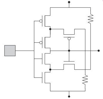
FIG. 20 Modified Schmitt trigger network for ESD improvement
9.1 Bipolar Single Ended Receiver Circuits
Receiver circuits are a common ESD sensitive circuit in Bipolar and BiCMOS technology.
Bipolar receiver circuits typically consist of npn bipolar transistor configured in a common emitter configuration (FIG. 21). For bipolar receivers, the input pad is electrically connected to the base contact of the npn transistor, with the collector connected to VCC either directly or through additional circuitry. The npn bipolar transistor emitter is electrically connected to VSS, or through a emitter resistor element, or additional circuitry.
In bipolar receiver networks, for a positive-polarity HBM ESD events, as the base voltage increases, the base-to-emitter voltage increases leading to forward biasing of the base- emitter junction. The base-emitter junction becomes forward active, leading to current flowing from the base to the emitter region. Typically in bipolar receiver networks, the physical size of the emitter regions are small. When the ESD current exceeds the safe operation area (SOA), degradation effects occur in the bipolar transistor. The bipolar device degradation is observed as a change in the transconductance of the bipolar transistor. From the electrical parametrics, the unity current gain cutoff frequency, fT, decreases with increased ESD current levels. From a fT-IC plot, the fT magnitude decreases with ESD pulse events, leading to a decrease in the peak fT.
For a negative pulse event, the base-emitter region is reverse biased. As the voltage on the signal pad decreases, the base-emitter reverse-bias voltage across the base-emitter metallurgical junction increases. Avalanche breakdown occurs in the emitter-base metallurgical junction, leading to an increase in the current flowing through the emitter and base regions; this leads to thermal runaway and bipolar second breakdown in the bipolar transistor. The experimental results show that the negative-polarity failure level has a lower magnitude compared to the positive-polarity failure level.
One common ESD design solution used to provide improved ESD results in a single ended bipolar receiver network is to place a p-n diode element in parallel with the npn bipolar transistor emitter-base junction (FIG. 22). Using a parallel element, the p-n junction is placed such that the anode is electrically connected to the npn emitter, and the cathode is electrically connected to the npn base region; this ESD element serves as a bypass element avoiding avalanche breakdown of the npn base-emitter junction. The diode element is placed local to the npn transistor element to avoid substrate resistance from preventing early turn-on of the ESD diode element. Note that this element is analogous to the CDM solution used in CMOS receiver networks. For a bipolar transistor, it is serving for events from both the signal pad and potential events from the emitter electrode.
In radio frequency (RF) bipolar receivers, metal-insulator-metal (MIM) capacitors are used between the signal pad and the base electrode. For positive- or negative-mode polarity events, the MIM capacitor can fail due to dielectric degradation. Without ESD protection on the receiver network, the ESD failure levels of the receiver network will be limited by the MIM capacitor element. An ESD solution to prevent ESD failure in these RF bipolar receivers is to use a p-n diode element in parallel with the MIM capacitor element. The p-n diode element can be in a reverse configuration so that it serves as a parallel capacitor element, and does not allow a dc voltage to be transmitted between the signal pad and the bipolar receiver base element. The functional disadvantage of the p-n element is the impact of the effective quality factor ''Q'' of the capacitor element.
9.2 Bipolar Differential Receiver Circuits
Differential receiver networks are used to improve the signal-to-noise ratio in bipolar networks. Differential receiver networks use a differential pair of identical npn bipolar transistors in a common-emitter mode. For differential bipolar receivers, two input pads are electrically connected to the base contacts of the identical npn transistors, and the two emitters are connected together. Below the emitter connection, additional circuitry, a current source or a resistor element is commonly used (FIG. 23).
FIG. 21 Bipolar receiver network
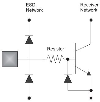
FIG. 22 Bipolar receiver network with ESD diode
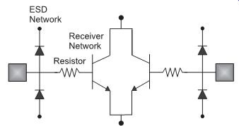
FIG. 23 Bipolar differential pair receiver network
One of the unique problems with differential receiver networks is pin-to-pin ESD failure mechanism. In ESD testing, we can apply an ESD pulse event to one of the two differential signal pads, using the second differential signal pad as the ground reference. In differential pair bipolar receiver networks, for a positive-polarity HBM ESD events, as the base voltage increases the base-to-emitter voltage of the first transistor leading to forward biasing of the base-emitter junction. The base-emitter junction becomes forward active, leading to current flowing from the base to the emitter region. For the second npn bipolar transistor, the base- emitter region is reverse biased. As the voltage on the first signal pad increases, the base- emitter reverse-bias voltage across the second transistor base-emitter metallurgical junction increases. Avalanche breakdown occurs in the emitter-base metallurgical junction, leading to an increase in the current flowing through the emitter and base regions; this leads to thermal runaway and bipolar second breakdown in the grounded second bipolar transistor of the differential pair. Note that the degradation of the second transistor prior to the first transistor can also lead to a differential offset hampering the matching of the two sides of the differential pair. It is possible that the failure criteria is associated with a npn mismatch prior to the ESD failure of either npn device.
An ESD design solution used to provide improved ESD results in a differential pair bipolar receiver network is to place a p-n diode element in parallel with the npn bipolar transistor emitter-base junction (FIG. 24). Using a parallel element, the p-n junction is placed such that the anode is electrically connected to the npn emitter and the cathode to the base region. In this fashion, an alternate forward-bias current path is established between both sides of the differential pair. Second, another method is to introduce a back-to-back diode string between both sides of the differential pair. This has the advantage of allowing a higher current between both sides of the differential pair, but the disadvantage of asymmetry matching and capacitance loading performance degradation. Additionally, a dual-emitter structure can be utilized where the first emitter is for functionality and the second emitter is for ESD protection [34].
10. SUMMARY AND CLOSING COMMENTS
In this Section, Section 7, receiver networks and ESD issues were discussed in fundamental CMOS and bipolar technology. The discussion focused on ESD implications of receivers as receiver networks evolved with technology generations and technology scaling. MOSFET scaling leads to an increase in complexity in receiver networks to address power supply scaling, threshold voltage scaling, MOSFET dielectric scaling and noise, as well as mixed signal interface environments. The transitions of the receiver networks lead to new ESD issues almost every technology generation. Additionally, feedback networks and pin-to-pin ESD issues were discussed in networks with hysteresis, feedback elements, and differential inputs became necessary. The focus of the Section addressed how to build a better receiver network with an increased ESD robustness by modification of the non-performance impacted circuit elements. The concepts and design practices are transferable to both bidirectional networks and other similar receiver circuits.
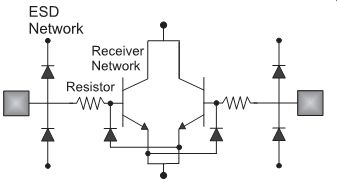
FIG. 24 Bipolar differential pair with ESD protection to avoid pin-to-pin
ESD failures.
Section 8, will address issues with SOI circuitry and ESD. Section 8, SOI ESD Circuits, addresses SOI circuits utilized in mainstream SOI application. The focus of the Section will be on integration of the SOI ESD networks in SOI microprocessors. In the Section, the evolution of the SOI ESD networks with the power supply scaling will be self-evident; as the power supply was reduced, technology innovation and scaling improved the ESD robustness of the SOI ESD structure. ESD learning led to more scaled and aggressive designs and architectural tricks, and ESD fault recognition led to improved SOI product results. Applying ESD design practices, such as gate decoupling for the SOI-gated diode structures, and the addition of decoupling from the power supply, additional improvements continued. The concepts are useful in the understanding of bulk CMOS receiver networks as well.
PROBLEMS
1. Assume a receiver network consisting of a pad, an n-channel half-pass transistor, and an inverter circuit. Assume that the n-channel half-pass transistor breakdown voltage to substrate is lower than the gate oxide breakdown voltage. Given that the n-channel half-pass transistor has a MOSFET width W, and conductance to substrate of value G per unit micron, show the voltage response of the circuit.
2. Assume a receiver network consisting of a pad, an n-channel half-pass transistor, and an inverter circuit. Assume that the n-channel half-pass transistor breakdown voltage, VBR, to substrate is higher than the gate oxide breakdown voltage, VOX. Assume the MOSFET snapback voltage Vt1 is less than the oxide breakdown voltage. What is the circuit response as a function of voltage?
3. Assume a receiver network consisting of a pad, an n-channel half-pass transistor, and an inverter circuit. Assume that the n-channel half-pass transistor breakdown voltage, VBR, to substrate is higher than the gate oxide breakdown voltage, VOX. Assume the MOSFET snapback voltage Vt1 is greater than the oxide breakdown voltage. What is the circuit response as a function of voltage?
4. Assume a receiver network consisting of a pad, a full-pass transmission gate (p-channel and n-channel MOSFET of equal width), and an inverter network. As a positive ESD pulse is applied, derive the current as a function of voltage across the full-pass transmission gate assuming current flows through the receiver dielectric according to CdV/dt. Does the n-channel MOSFET undergo MOSFET snapback? What size should the p-channel MOSFET be in order to prevent n-channel MOSFET snapback in the full pass transistor network? Take into account the p-channel MOSFET as a diode-resistor element or pnp transistor.
5. Assuming a receiver network consisting of a pad, an n-channel MOSFET transmission gate, an inverter, and a p-channel MOSFET keeper feedback element of width W. Show the circuit schematic highlighting the parasitic diode formed between the p-channel MOSFET keeper drain and its corresponding n-well. Assuming an n-well resistance value associated with the width W, and n-well sheet resistance, and modeling the keeper network as an ideal diode and well series resistor, derive the current and voltage relations across the n-channel MOSFET transmission gate when the VDD is grounded. What well-resistor value is needed to avoid the failure of the n-channel MOSFET half-pass transistor? Given that an additional resistor is placed between the p-channel MOSFET keeper drain and the n-channel MOSFET half-pass node, what resistor value will prevent the MOSFET half-pass transistor from failing?
6. Given a receiver network consisting of a pad, an n-channel MOSFET transmisson gate, and a receiver network, list all the possible failure mechanisms and current paths to failure from HBM, MM, and CDM events.
7. Given an SOI receiver network consisting of a pad, an n-channel SOI MOSFET transmission gate, and a SOI receiver network, list all the possible failure mechanisms and current paths to failure from HBM, MM, and CDM events. Evaluate positive and negative polarity to both VDD and VSS . How does this differ from the bulk implementation? Which is more robust? How does the charge get back to the input pad for CDM mechanisms?
8. Given an SOI ESD network and an SOI receiver network, consisting of a pad, a SOI double-diode network (whose gate is connected to their respective cathode nodes), a SOI n-channel pass transistor and a SOI receiver network. Evaluate positive and negative polarity to both VDD and VSS. List all possible failure mechanisms, and current paths to failure from HBM, MM, and CDM events.
9. In SOI technology, the substrate region below the buried oxide is electrically disconnected from the thin silicon film above the buried oxide region. Does providing an electrical contact between the substrate and the substrate power rail make CDM mechanisms better or worse? How will the failure mechanisms change?
10. Assume a receiver network with a n-channel zero-threshold voltage transmission gate between the pad and the inverter. What is better for ESD-a zero VT device or a non zero VT device?
Prev. | Next