Signal tracing is the procedure by which the progress of an applied signal voltage is checked, stage by stage, through the signal channels of a television receiver. The signal channels consist of an rf amplifier, mixer, video-i-f amplifier, video amplifier, sound i-f amplifier, and audio amplifier.
TROUBLESHOOTING RF AMPLIFIER
When the symptom is "no picture and no sound," signal tracing starts logically at the tuner-after tubes have been checked, of course.
A typical tuner configuration using tubes is shown in Fig. 4-1. A transistor-type tuner is shown in Fig. 4-2. The same functions are performed by both the tubes and the transistors. However, the dc voltages in a transistor tuner are comparatively low. Note also that the grid of an rf amplifier tube, for example. draws practically no current, whereas the base of an rf amplifier transistor draws appreciable current.
The test point (often called the looker point) is a convenient terminal from which to make a preliminary signal-tracing test. A low-capacitance probe and scope are connected to it, and the tuner input terminals are energized from a tv antenna or from a pattern or signal generator. If the scope has good sensitivity. about an inch of vertical deflection will normally be obtained from a fairly strong input signal.
When a pattern generator is used, the video waveform in Fig. 4-3 will normally be observed.
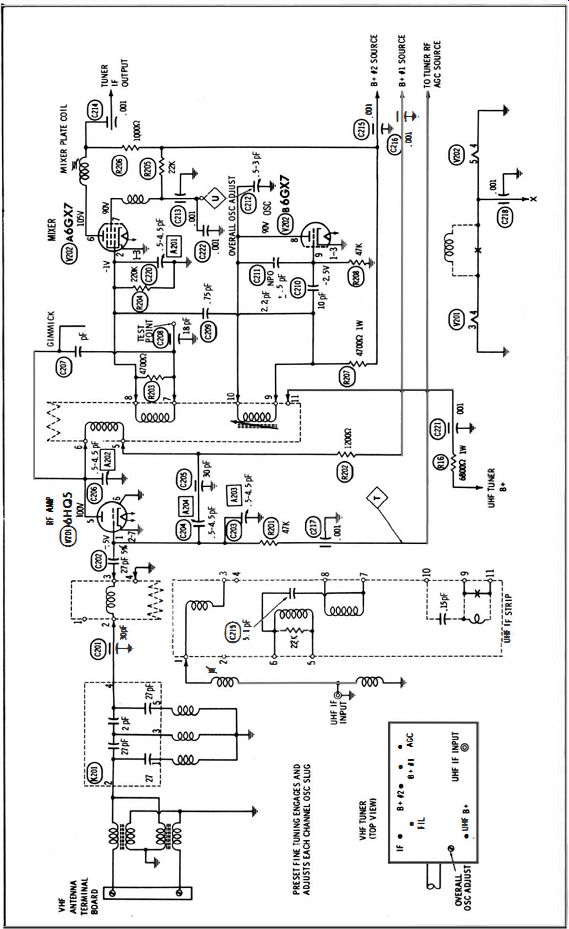
Fig. 4·1. Typical tuner configuration using tubes.
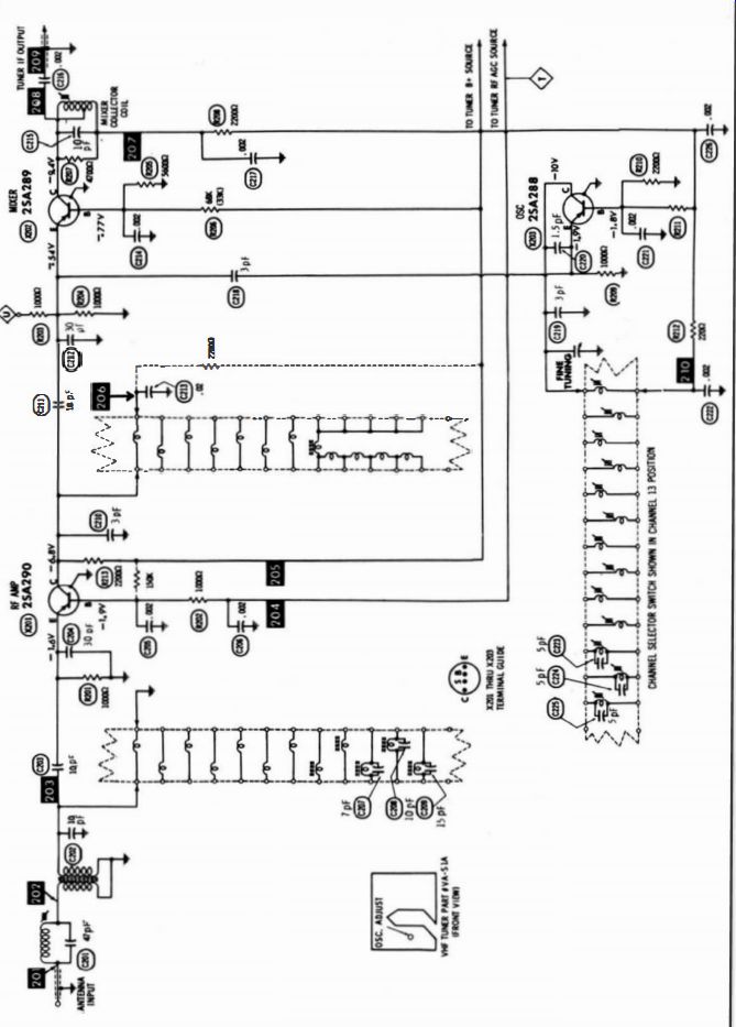
Fig. 4-2. Typical transistor-type tuner.
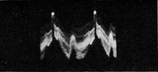
Fig. 4-3. Video waveform present at the looker point.
If the scope sensitivity is low, a direct probe can be applied to the looker point-although the increased circuit loading will add to the waveform distortion. Even with a low-C probe, the reproduced video waveform has appreciable distortion because the looker point is a tap on the mixer grid-leak. Thus, between the mixer grid and the probe there is series resistance, which acts as a low-pass filter. The horizontal-sync pulses are attenuated considerably, and the high-frequency components of video information are lost. Nevertheless, the significant consideration is the presence or absence of the signal. If the signal is absent, the tuner components must be checked. Voltages can be measured with a vom or vtvm, and resistors with an ohmmeter.
Capacitors must be removed from the circuit and checked on a tester (or by substitution). When components are inconveniently "buried" in a tuner, many technicians prefer to send it to a specialty shop for repair.
There is a reason for using a low-C or direct probe instead of a demodulator probe at the looker point. The mixer is a heterodyne configuration in which the grid circuit operates basically as a rectifier and not as an amplifier. (There is a small gain through the mixer stage, but this is not its primary function.) The grid normally operates at zero bias (or contact potential). Should a dc bias voltage be fed to the grid, the tube would be biased to the midpoint of its characteristic and operate as an amplifier instead of detector. No i-f signal would appear at the plate and, for all practical purposes, the mixer would be dead.
A substantial negative bias will appear on the mixer grid during normal operation. It is generated by grid current during positive peaks of the oscillator signal, which is injected into the mixer grid circuit.
This signal-developed bias provides a good check of oscillator operation. If a vom or vtvm measures zero volts or only the contact potential (about -0.5 volt), the oscillator stage is dead.
When no signal is found during a scope check at the looker point, do not forget to measure the agc voltage to the rf amplifier. Trouble in the agc line can bias off (cut oft) the rf amplifier tube, and thereby give a false appearance of tuner trouble. The agc voltage should measure nearly zero volts with no signal input to the tuner. With an applied signal, several volts of negative bias will be measured when the signal level is turned up.
If a tv station signal is used, a changing video waveform will normally be displayed at the looker point. The signal has the basic appearance shown in Fig. 4-3. If an a-m signal generator is used to drive the tuner, a sine-wave signal will normally be observed at the looker point (Fig. 4-4). The waveform may or may not appear distorted, depending on the signal generator being used. Some a-m generators have a good sine-wave modulation, while others have a highly distorted waveform. Distorted modulation is not of concern; only the presence or absence of a signal is checked for at the looker point.
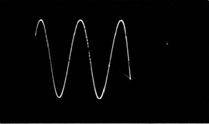
Fig. 4-4. An a-m generator displays a sine-wave signal.
The detector action of a mixer tube is indicated in Fig. 4-5. Partial rectification is illustrated. The modulated rf input signal has an average value of zero, because the positive and negative half-cycles have equal excursions. The output signal, however, does not have an average value of zero. It has a dc component on which the modulating frequency component is superimposed. The modulating frequency is comparatively low, and falls within the response range of the scope. Hence, the modulating frequency waveform is seen on the scope screen.

Fig. 4-5. Detection process in mixer tube. (A) Modulated rf input to mixer.
(B) Partial rectified output contains the modulation.
SIGNAL TRACING IN THE I-F SECTION
A demodulator probe is used to signal-trace the video i-f section.
Fig. 4-6 shows a simplified video i-f circuit, with successive test points lettered. The lowest signal level occurs at point A, and the highest at point H. The normal signal level at point E will be greater than the normal level at point D, because of the stage gain. However, when making demodulator probe tests, the reverse may seem to be the fact.
Input capacitance of the probe causes circuit detuning.
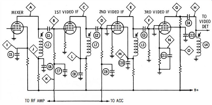
Fig. 4-6. A three-stage video i-f amplifier.
It is helpful to make signal-tracing tests with a signal generator instead of a tv broadcast signal, because you can adjust the level of the generator signal as required. Unless you use a very high-gain scope, a fairly high-level signal is required to check the first i-f stage with an ordinary demodulator probe. If you use an a-m signal generator, the signal-tracing pattern appears as illustrated in Fig. 4-7 A. A sweep-generator signal is also useful, and the signal-tracing pattern appears as shown in Fig. 4-7B. A test-pattern generator can also be used in lieu of a tv broadcast signal.
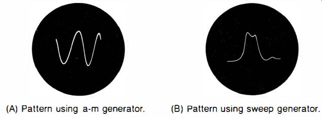
Fig. 4-7. Typical signal-tracing patterns. (A) Pattern using am generator.
(B) Pattern using sweep generator.
Most i-f amplifiers are stagger-tuned. In case L3 is tuned to a lower frequency than L2, application of the probe at point E temporarily makes the resonant frequency of L3 still lower. The impedance of the L3 plate-load circuit becomes abnormally low. The stage may appear to have a loss instead of a gain. Hence, do not consider apparent gain indications as meaningful, and look merely for the presence of a signal. A typical pattern is shown in Fig. 4-8. The scope is deflected at a 30-Hz rate. The pattern is distorted because of limited probe bandwidth, and the vertical sync pulse is the most prominent element in the pattern.
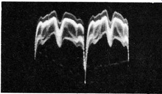
Fig. 4-8. Typical pattern obtained in an i-f signal-tracing test.
In the example cited, wherein L2 is tuned to a higher frequency than L3 (Fig. 4-6), applying the probe at point D may cause the i-f stage to break into oscillation. This occurs when the probe's input capacitance lowers the resonant frequency of L2 to about the same value as L3. The stage then operates as a tuned-plate tuned-grid oscillator. No pattern appears on the scope screen, because the stage is blocked by the high signal-developed bias resulting from oscillation.
Thus, the stage may seem to be dead when tested at point D, but the false conclusion is avoided by observing that a signal is found at point E.
If a signal is found at point C but not at point D, this indicates that coupling capacitor C2 is open. Little or no signal is normally found at decoupling points, such as I, J, K, etc. Do not be misled by the presence of a small signal at decoupling points. It is difficult to get a perfect ac ground at 40 MHz because of the series inductance of connecting leads. Thus, unless the leads of the decoupling capacitor are very short, bypass action is somewhat incomplete. When a stage does not check out satisfactorily in the signal-tracing test, individual components in the stage are tested next. Voltages and resistances are measured and compared with values specified in the receiver service data. Capacitors are tested on a capacitor checker, or by substitution.
Poor Picture Quality

Fig. 4-9. A poor picture-quality symptom.
Fig. 4-10. Bandwidth is measured between the 6-dB points.
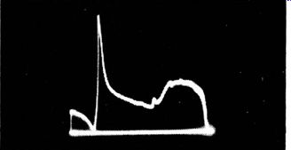
Fig. 4- 11 . A sharp peak on a response curve causes ringing.
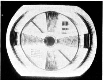
Fig. 4-12. Distortion caused by i-f regeneration.
Trouble in the i-f amplifier can cause a poor picture-quality symptom, as illustrated in Fig. 4-9. If a laboratory-type (wideband) demodulator probe is available, the defective stage can be located directly by a signal-tracing procedure. The video signal is inspected for distortion as the probe is moved progressively through the i-f amplifier section. If a service-type demodulator probe is used, the video signal will be so severely distorted that the needed indication is masked. Therefore, an indirect troubleshooting method must be used.
A sweep generator is used instead of a pattern or signal generator.
Good picture quality depends on adequate bandwidth and a reasonably flat-topped frequency response. Fig. 4- 10 shows how bandwidth is measured between the 6-dB (half-voltage) points. A bandwidth of at least 3 MHz is required for acceptable picture quality. If the top is not reasonably flat, but is sharply peaked as in Fig. 4- 11 , picture quality will be poor even when bandwidth is adequate. A sharp peak causes ringing in the picture (circuit ghosts).
Ringing appears as illustrated in Fig. 4-12. As you turn the fine tuning control, the pattern changes rapidly. This occurs because the picture i-f carrier is being moved up or down on the i-f response curve.
If you bring your hand near the i-f tube(s) which are in the regenerative circuit, the pattern will again change rapidly. Because the i-f response curve is so sharply peaked (Fig. 4- 11), a small change in stray capacitance shifts the ringing frequency considerably. Regeneration is also responsive to signal-level (agc bias) changes. The reason for this dependency is that the sharpness of the peak depends greatly on the amount of i-f signal being fed back. When the i-f gain is reduced, less i-f voltage is fed back. This reduces the amplitude of the peak and increases the bandwidth.
When the distorting stage is localized, the dc voltages and resistances in the circuit are measured, capacitors are checked, and the stage alignment is investigated. Alignment of the tuned circuits is usually checked last, because poor picture quality is most likely to be caused by a defective component. There is usually only one defective component to be localized. If a screen bypass capacitor is shorted, however, it sometimes damages the screen resistor also, because of excessive current drain. (The undistorted video signal is shown in Fig. 4-13.)

Fig. 4-13. Undistorted video signal.
Picture Pulling, or Loss of Sync
When an i-f tube is overloaded, the sync pulses are always compressed or clipped, as seen in Fig. 4-14. Overloading is usually caused by the grid or cathode bias being too low. Thus, if C11 or C9 becomes shorted (Fig. 4-6), sync compression can be expected. Of course, it is assumed that i-f amplifier tubes are good. Vertical sync punching is often observed when bias on an i-f tube is too low. The vertical sync pulse is depressed below the level of the horizontal pulses. Sync punching causes unstable vertical sync, or complete loss of vertical lock.
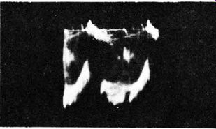
Fig. 4-14. Sync pulses compressed.
Severe overloading in an i-f stage can cause a negative picture when the grid-leak resistance is comparatively high. When a picture is completely negative, all the tones are reversed. When it is partially negative, the deep grays and blacks are reversed in tone, while medium and light grays are reproduced normally. Negative picture reproduction is caused by modulation reversal, whereby positive modulation is converted to negative modulation. Excessive grid current, with suitable circuit constants, results in this conversion.
Hum in the I-F Signal
Two types of hum voltage can enter the video signal. Power-supply hum may be either 60-Hz or 120-Hz frequency, depending on the type of power supply. Heater hum has a 60-Hz frequency. A scope is a sensitive indicator of hum, showing clearly the presence of hum voltage at levels below the point at which hum bars appear in the picture.
When the hum level is high, the video signal appears typically as shown in Fig. 4-15, and the picture contains hum bars as in Fig. 4-16.
Sync stability is often affected when the hum level is high.

Fig. 4-15. Hum in the video i-f signal.
Fig. 4-16. Strong hum bar in picture.
Basically, 60-Hz hum produces one cycle of sine-wave curvature in the video signal, while 120-Hz hum produces two cycles. The pattern is not always simple; agc action tends to smooth out the hum, and amplification becomes non-linear when the hum level is high, distorting the hum waveform. Only heater hum has a sine-wave shape; power-supply hum usually has a distorted sawtooth waveshape.
To trace hum voltage to its source in an i-f amplifier, it is usually necessary to clamp the age line with a bias box or battery. Doing so eliminates the confusion of agc reaction, and the video signal will be normal until the stage injecting the heater hum voltage is reached. Thus, heater hum is easily and definitely localized in a signal-tracing test.
Power-supply hum, however, is a generalized source which feeds into all the i-f stages. The hum component increases from stage to stage, and has its lowest amplitude at the first i-f grid. When power supply hum is suspected, use a low-C probe with the scope, and check for hum on the B+ supply line. There is always some hum voltage present, but it should not be greater than the value specified in the receiver service data.
If normal reception resumes when the agc line is clamped, the hum voltage is entering the i-f amplifier via the agc line. The trouble then will be found in the agc section, and not in the i-f section. Do not confuse hum voltage on the agc line with 60-Hz variations stemming from sync-section trouble. For example, if a fault in the afc circuit causes the picture to pull considerably at the top, a loss of phase will occur between grid and plate pulses in a keyed-agc tube, and a 60-Hz voltage simulating hum will appear on the agc line.
Low Contrast Versus Stage Gain
Low contrast in the picture (Fig. 4-17) is due to low gain. It is sometimes necessary to localize a low-gain i-f stage, to clear up a symptom of low contrast. Localization is uncertain with a demodulator-probe test because of the erratic nature of circuit loading imposed by ordinary probes. However, by using the picture detector as the demodulator, and by using an i-f signal-injection technique, a low gain stage can be quickly localized.
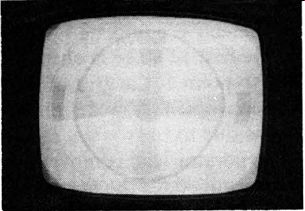
Fig. 4-17. Picture has low contrast.
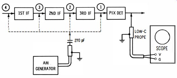
Fig. 4-18. Stage-gain test setup.
The test setup illustrated in Fig. 4- 18 can be used. Connect a scope and low-capacitance probe to the picture-detector output to serve as an indicator. Use an a-m generator as a signal source, and connect a 270-pF blocking capacitor in series with the "hot" lead, to avoid drain-off of dc bias. Clamp the agc line with -1 . 5 or -3 volts dc from a bias box or battery, and apply the generator signal first at point 1 to drive the input of the picture detector. Operate the generator on its modulated-output function, tune to the mid-frequency of the i-f band, and advance the generator output to produce about a half inch of vertical deflection on the scope screen. (This is a sine-wave pattern.) Next, transfer the "hot" lead from the generator to point 2, the grid of the third i-f tube. In case the third i-f stage is operating normally, the sine-wave pattern on the scope screen will increase in height considerably. With -1.5 volts of bias, a gain of 5 is typical; however, the exact stage gain differs depending on the tube type and circuitry details. If the third i-f stage is faulty, the pattern will increase only slightly in height, or may even decrease. In such case, check out the components in the third i-f stage.
The next test is made by connecting the "hot" generator lead to point 3, the grid of the second i-f amplifier. If the pattern is off-screen vertically, go back to point 2 and reduce the generator output for a suitable pattern height, such as .5 inch. Then transfer the generator lead to point 3, and observe how many times the pattern height increases. Again, a substantial gain should be found. Otherwise, there is a defective component in the second i-f stage.
The first i-f stage is checked for gain by transferring the generator lead to point I, the grid of the first i-f amplifier. This progressive test procedure will show definitely whether a low-contrast picture symptom is due to i-f trouble, and, if so, which stage is at fault. Each time the generator lead is moved back one stage, the true gain of the stage is determined for the particular grid-bias voltage to which the agc line is clamped.
This procedure gives a true gain figure, because the a-m generator has low output impedance (the output cable is terminated usually in either 50 or 75 ohms). When the generator signal is applied to the grid of an i-f tube, the low impedance of the source "swamps out" the resonant response of this grid circuit, and the following i-f circuitry operates normally.
Ground-Circuit Difficulties
Although ordinary low-impedance demodulator probes are not susceptible to stray-field interference, extended ground loops can cause application problems in low-level circuits such as the first video i-f stage. In Fig. 4- 19, for example, when the signal is checked at point A, a different pattern may be observed if the probe is grounded at point 2 instead of at point 1. The reason is that the separated ground points have appreciable reactance between them at 40 MHz. If the probe is grounded at point 2, the voltage difference between points 1 and 2 is added to the grid waveform. Obviously, if the demodulator probe is connected between grounds 1 and 2, the probe input will not be short-circuited. Instead, a waveform will be seen on the screen when the scope is operated at high gain. The farther a pair of 40-MHz grounds is separated, the greater the ground-circuit interference.
Some i-f amplifiers have a common ground point for all components within a given stage. In such case, the possibility of ground-circuit pickup is not present. However, this is not true of all i-f strips, as ground points for grid and plate circuits may be several inches apart in some chassis. The most troublesome ground-circuit interference occurs when the probe is moved from one stage to the next without transferring the probe ground lead. That is, the signal is being checked in the first i-f stage, for example, but the probe ground is connected to the chassis at the output of the second stage. This is poor practice, because the ground-circuit drop may introduce more signal voltage than is present at the first i-f grid.
Signal-Injection Precautions in Transistor I-F Strips
A typical transistor i-f strip is shown in Fig. 4-20. Although the dc voltages are much lower than in a tube-type i-f amplifier, the signal levels are not greatly different in normal operation. Hence, signal tracing is essentially the same in both types of amplifiers.
When a signal is injected into a transistor i-f strip, damage to transistors must be avoided. An a-m signal generator may have a substantial 60-Hz output voltage unless the ground lead is connected to the receiver chassis. Therefore, connect the ground lead first, and remove it last. Another precaution is to use a blocking capacitor in series with the "hot" lead of the generator; otherwise, drain-off of base bias can damage the transistor in some i-f configurations. The same precautions apply when a test-pattern signal is injected from a tv analyzer.
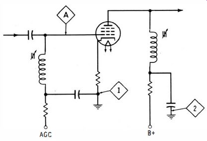
Fig. 4-19. Grounds (1) and (2) are at different 40-Hz potential.
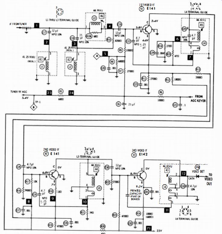
Fig. 4-20. Typical transistor i-f amplifier.
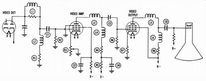
Fig. 4-21. Typical video amplifier.
SIGNAL TRACING IN THE VIDEO AMPLIFIER
A low-C probe is used when signal-tracing in the video-amplifier section. Fig. 4-2 1 shows a typical circuit for the video-amplifier section. This is an ac coupled amplifier. Some video amplifiers are dc coupled, and many utilize only one stage. The coupling capacitors in ac coupled amplifiers are checked easily in the signal-tracing procedure. Fig. 4-22 shows how a low-C probe is shifted from input to output of a coupling capacitor in this test. Practically the same undistorted video signal is found normally at either end of the capacitor.
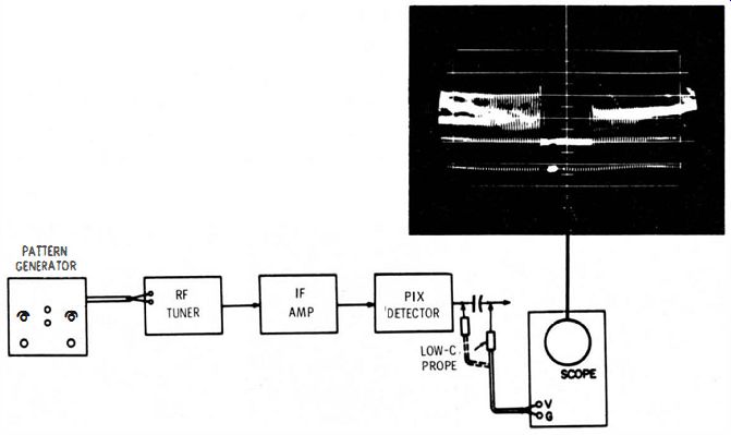
Fig. 4-22. Signal tracing across a coupling capacitor.
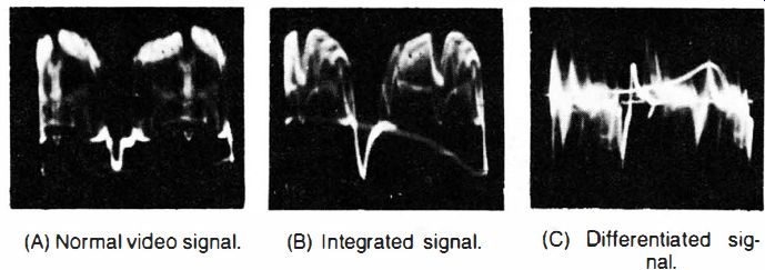
Fig. 4-23. Normal and abnormal video waveforms in Fig. 4-21. (A) Normal video
signal. (C) Differentiated signal. (B) Integrated signal.
If the capacitor is open or nearly open, the video signal will be normal at the input end, but differentiated at the output, as shown in Fig. 4-23. If a good capacitor is bridged across the open unit, the output waveform will be restored to normal. Thus, the scope and low-C probe serve as an efficient in-circuit capacitor checker.
In case an integrated video signal is observed, as shown in Fig. 4-23B, decoupling capacitor C4 (Fig. 4-21) will be the suspect. The suspicion is confirmed by checking across C4 with the probe. If a video signal is present, the capacitor is open. An open decoupling capacitor causes integration of the video signal because the plate-load resistance is thereby abnormally increased. In turn, high video frequencies are attenuated and shifted in phase. Phase shifts in the video signal cause picture smear.
In order to see clearly the nature of frequency distortion and phase shift in a video signal, it is helpful to observe a simplified waveform consisting of a hybrid sine and square wave, as seen in Fig. 4-24. This waveform normally consists of a section of sine wave followed by a section of square wave. When differentiated, the flat top becomes curved downward, showing the loss of low frequencies. Also, the sine-wave section is shifted in phase and leads the normal wave. The flat top becomes curved upward when integrated, showing the loss of high frequencies. The sine wave section is shifted in phase and lags the normal wave.
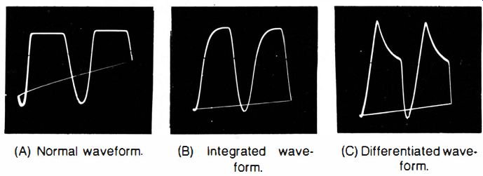
Fig. 4-24. Hybrid sine and square waves. (A) Normal waveform. (B) Integrated
waveform. (C) Differentiated waveform.
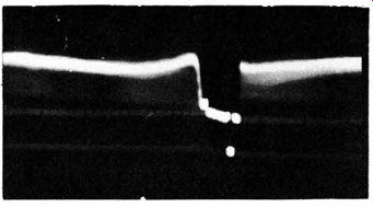
Fig. 4-25. Video signal with white portions compressed.
White Compression
When incorrect operating voltages cause a video-amplifier tube to compress or clip the video signal in the white region (Fig. 4-25), the picture appears muddy and filled up. On the other hand, compression or clipping of the sync tips causes impaired sync lock. Although sync clipping can occur in either the video amplifier or the i-f amplifier, white compression occurs only in the video amplifier.
If white compression is localized to a stage, check the dc voltages at the video-amplifier tube(s). Incorrect grid or cathode bias is the most common cause, although off-value plate and screen voltages are sometimes responsible. A leaky coupling capacitor or a shorted cathode-bypass capacitor changes the grid and cathode bias voltages, respectively. Off-value plate or screen voltages are usually caused by resistors increasing in value (although a resistor occasionally decreases in value). A leaky screen bypass capacitor reduces the screen voltage, and a leaky plate-decoupling capacitor reduces the plate voltage. An open screen bypass capacitor causes a greatly reduced gain figure, and the picture has low contrast.
Gain is checked quickly by comparing vertical deflections at the input and output of the video amplifier. Since normal gain figures vary considerably from one chassis to another, check the receiver service data. Peak-to-peak voltages at the video-amplifier output and input are specified. If the gain is normal but the peak-to-peak voltages are low, the trouble is in a stage ahead of the video amplifier.
Poor Definition
If poor picture definition occurs in the video amplifier, a signal-tracing test with square-wave input will disclose the faulty circuit. The output from a square-wave generator is applied at the video-detector output terminal, and a low-C probe is connected to the video amplifier output terminal. Poor-definition picture, sweep-frequency response, and 100-kHz square-wave symptoms are shown in Fig. 4-26.
The attenuated high-frequency response in the sweep-frequency pattern and the rounded corners in the 100-kHz square-wave pattern correspond to the "wiped out" vertical wedges in the test pattern.
The symptoms shown in Fig. 4-26 throw suspicion on the load resistors or peaking coils in a branch of the video amplifier. Remember that the video-detector output circuit is also the video-amplifier input circuit. Therefore, if the video-detector load resistor increases in value considerably, the symptoms seen in Fig. 4-26 appear. The square-wave signal-tracing procedure is useful because the distorted response is first found at the defective circuit branch.
A peaking coil is sometimes shunted by a damping resistor, as indicated in Fig. 4-2 1. If the peaking coil opens, the circuit will still be operative through the damping resistor. However, high-frequency distortion will be severe, square-wave corner rounding will be evident, and the picture will be badly smeared. If a damping resistor opens or increases greatly in value, the usual symptom is square-wave overshoot (Fig. 4-27). A small amount of overshoot is not objectionable, and has the effect of sharpening the edges of objects in the picture, particularly when old movie films are being televised. However, excessive overshoot causes an objectionable "outlining" of sharp edges in an image.
When the chassis has a one-stage video amplifier, the tube must be driven to maximum output to obtain normal picture contrast.
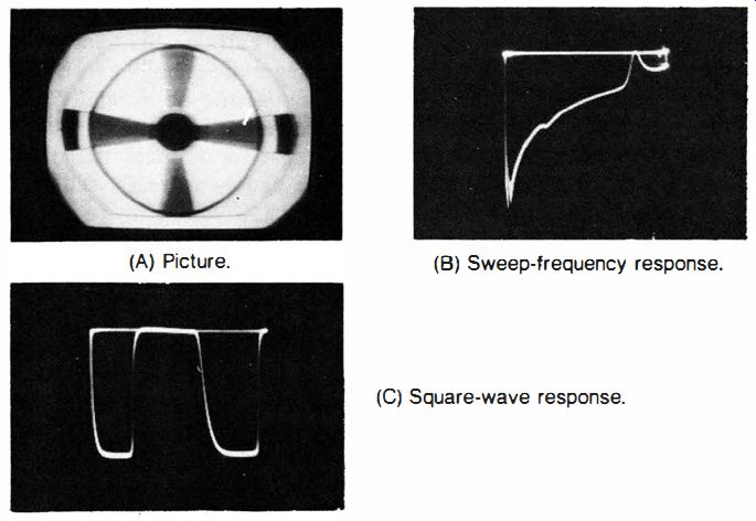
Fig. 4-26. Picture, sweep-frequency, and 100-kHz square-wave symptoms. (A)
Picture. (B) Sweep-frequency response. (C) Square-wave response.

Fig. 4-27. Square wave with overshoot.
Fig. 4-28. Square wave that has an unsymmetrical overshoot.
Unless adequate screen and plate voltages are supplied to the tube, full contrast may require driving the grid into grid current on positive peaks. In that case, any overshoot arising in the grid-circuit branch will appear as an unsymmetrical overshoot (Fig. 4-28). On positive peaks of drive signal, the low grid-circuit impedance damps the peaking-coil response excessively, and the leading corner of the square wave is rounded. On the other hand, during negative peaks of drive signal, the grid-circuit impedance is high and the peaking-coil response is undamped by the tube.
Ringing and Circuit Ghosts
In case the plate-load resistor of a video-amplifier tube decreases in value considerably, the high-frequency response will rise excessively. In turn, a square-wave signal displays both overshoot and ringing, as in Fig. 4-29. Here, the ringing is more prominent on the trailing edge, due to grid-current generated by the leading edge. Ringing produces "repeats," or circuit ghosts, in the picture.
Excessive high-frequency response implies subnormal low-frequency response. This results in more or less tilt in the top of the square wave. The picture symptom is smearing or lack of a solid tone in large objects in a scene. Severe tilt is apparent in Fig. 4-29, along with the overshoot and ringing.
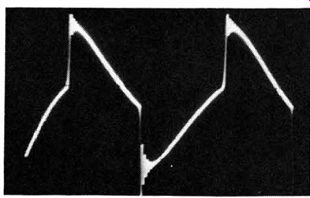
Fig. 4-29. Differentiation, ringing, and overshoot in a reproduced square
wave.
A valid check for ringing cannot be made unless the square-wave generator has a sufficiently fast rise time. The rise time of the generator should be at least as fast as that of the video amplifier. According to a rough rule of thumb, the rise time of an amplifier is given by one-third of the period corresponding to the frequency 3 dB down at the high end of the amplifier's response. In other words, if a video amplifier has a 4-MHz bandwidth, the corresponding period will be 0.25 microsecond, and the rise time will be about 0.08 microsecond. Hence, the square-wave generator should have a rise time of 0.08 microsecond or less for a useful ringing test.
Square-wave tests are also useful for evaluating the performance of a transistor video amplifier. Fig. 4-30 shows the configuration of a typical transistor video amplifier. The test setup is made as shown in Fig. 4-3 1. Although it is not essential to disconnect the video detector diode, doing so will reduce the loading on the square-wave generator and help to obtain a better input waveform. Be careful to avoid overdrive in the case of a transistor video amplifier, because transistors are much more easily damaged than tubes. The output from the square-wave generator should be not more than 1 volt peak to peak.
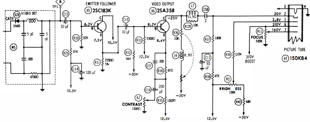
Fig. 4-30 Video amp
In theory, a video amplifier should reproduce a perfect square wave. However, in practice, distortion is always present; the less the distortion, the better the performance of the amplifier. Fig. 4-32 illustrates the 100-kHz square-wave response of a high-performance video amplifier. This type of response is normally observed in color tv and in deluxe black-and-white video amplifiers. The leading edge of the reproduced square wave may be expanded if a triggered-sweep scope is used (Fig. 4-33), and the rise time measured by means of the calibrated sweeps. Rise time is related to bandwidth by the formula BW =0.3S/T, where BW is the bandwidth in Hz, and T is the rise time in seconds (actually, a small fraction of a second).
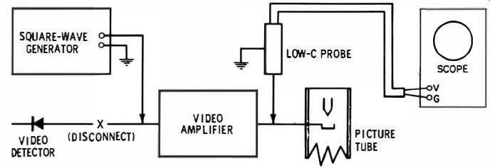
Fig. 4-31. Test setup.
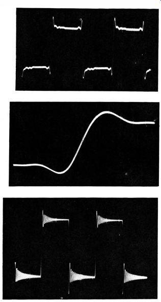
Fig. 4-32. Normal 100-kHz square-wave response of a high-performance video
amplifier.
Fig. 4-33. Expanded leading edge.
Fig. 4-34. Typical 100 kHz square-wave response of an economy-type video amplifier.
Economy-type video amplifiers normally exhibit appreciable ringing, as illustrated in Fig. 4-34. This ringing (along with overshoot) is accepted in order to obtain a reasonably fast rise time. In general, overshoot should not exceed 10 percent. The rise time should be on the order of 0.08 microsecond. If overshoot is excessive, or if the rise time is appreciably slower than normal, check the peaking coils, load-resistor values, bypass capacitors, and decoupling capacitors. It is advisable to check peaking coils by substitution.