AMAZON multi-meters discounts AMAZON oscilloscope discounts
The conventional electronic power supply is designed to provide a d-c output voltage from an applied a-c input voltage. The job of converting the alternating current to direct current is performed by the power-supply rectifier. There are four basic power-supply rectifier arrangements: half-wave, full-wave, bridge, and voltage multiplier.
THE HALF-WAVE RECTIFIER
FIG. 1 shows the basic operation of the half-wave rectifier. In FIG. 1A the a-c voltage is applied to the primary of transformer T1 so that the top of the secondary is positive with respect to the bottom.
Under this condition the plate of rectifier tube V1 is positive with respect to the cathode. Electrons flow from the cathode to the plate, through the secondary winding of T1, and through the load, as indicated by the arrows.
In FIG. 1B, the a-c voltage applied to the primary of T1 has re versed so that the top of the secondary is now negative with respect to the bottom. The plate of V1 is now negative with respect to the cathode, so no electrons flow from cathode to plate, and there is no current in the secondary of T1 and the load. (Remember, the plate of a vacuum tube must be positive with respect to the cathode for electrons to be attracted to the plate from the cathode). On the next half-cycle of the supply, the plate is again positive with respect to the cathode, and electrons again flow through V1, the secondary of T1, and the load. From this you can see that a series of current pulses is produced through the load. These pulses are of such a polarity that the cathode end of the load is positive with respect to the bottom end, as shown in FIG. 1A.
FIG. 2 shows another variation of the basic half-wave rectifier. In this circuit, rectifier V 1 has been reversed so that its cathode is connected to the top of the secondary winding of T1. In FIG. 2A, the top of the secondary is negative with respect to the bottom, and as a result, the cathode is negative with respect to the plate. (This is the same as saying the plate is positive with respect to the cathode.) Electrons flow from the cathode to the plate; the resulting current in the circuit is indicated by the arrows. Note that the bottom of the load is now positive with respect to the top-just the reverse of FIG. 1A. In FIG. 2B, the upper end of the secondary is positive with respect to the bottom end, so the cathode is positive with respect to the plate.
No electrons flow from cathode to plate, and there will be no current in the circuit. FIG. 2C shows the series of negative pulses developed across the load.
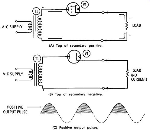
FIG. 1. Operation of half-wave rectifier (positive output). (A) Top of
secondary positive. (B) Top of secondary negative. (C) Positive output
pulses.
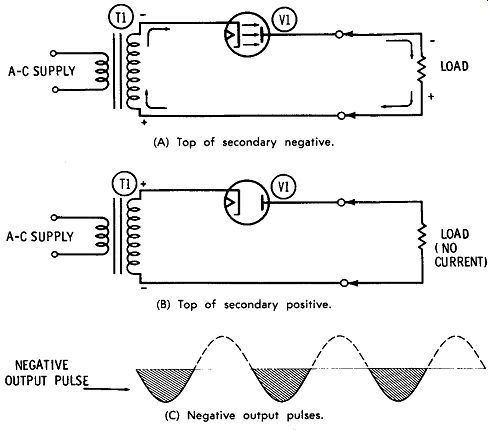
FIG. 2. Operation of half-wave rectifier (negative output). (A) Top of secondary
negative. (B) Top of secondary positive. (C) Negative output pulses.
THE FULL-WAVE RECTIFIER
FIG. 3 shows the basic operation of the full-wave rectifier. Notice that the full-wave rectifier differs from the half-wave rectifier in that two rectifier tubes are required and that the secondary of T1 is center tapped.
In FIG. 3A, the a-c voltage applied to the primary of T1 is such that the top of the secondary is positive with respect to the center tap, and the bottom of T1 is negative. Under these conditions, the plate of V1 is positive with respect to the cathode, and electrons flow through V1, the top half of the T1 secondary, and the load. Since the plate of V2 is negative with respect to the cathode, there is no current in V2.
In FIG. 3B, the a-c voltage applied to the primary has reversed so that the top of the T1 secondary is now negative with respect to its center tap, and the bottom is positive with respect to the center tap.
Now the V2 plate is positive with respect to the cathode. Electrons flow through V2, the bottom half of the secondary, and the load, as indicated by the arrows.
FIG. 3C shows the resulting series of current pulses in the load.
Note that the "gaps" in the pulses produced by the half-wave rectifier ( FIG. lC) are filled in by the full-wave rectifier. This results in a smoother current through the load, because the full-wave rectifier produces an output for both alternations of applied voltage, while the half-wave rectifier produces an output for only the positive or the negative half-cycles.
One disadvantage of the full-wave rectifier is that the transformer secondary, being center-tapped, must generally have twice as many turns as a half-wave rectifier transformer giving the same voltage output. However, the output of the full-wave rectifier is much easier to filter ( smooth out) because both alternations are used.
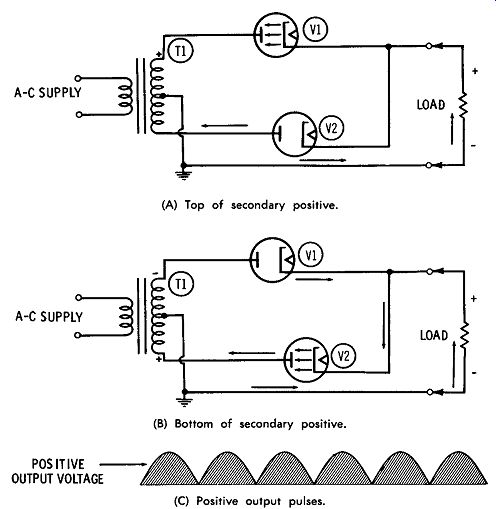
FIG. 3. Operation of full-wave rectifier.
(A) Top of secondary positive.
(B) Bottom of secondary positive.
(C) Positive output pulses.
THE BRIDGE RECTIFIER
The bridge rectifier is similar to the full-wave rectifier in that it provides a d-c output for both half-cycles of the applied a-c input. however, the full-wave rectifier requires only two rectifier tubes, whereas the bridge requires four. Also, the bridge rectifier does not use a center-tapped secondary winding, and the full-wave rectifier does. The entire secondary is used on both alternations in the bridge circuit.
FIG. 4 explains the operation of the bridge rectifier. In FIG. 4A, the a-c input to transformer T1 makes the top of the secondary positive with respect to the bottom. Since the plate of V1 is positive with respect to the cathode, electrons are attracted from the cathode to the plate. This causes a current in the T1 secondary, V2, the load, and finally, V1, as indicated by the arrows.
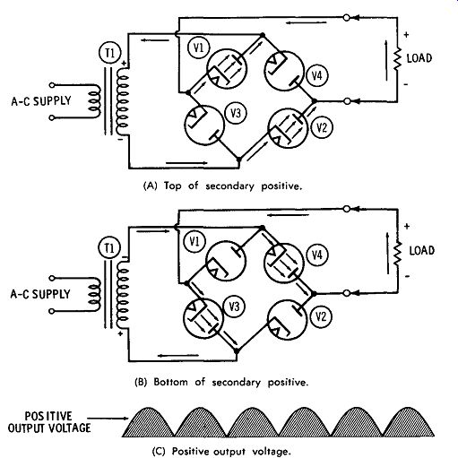
FIG. 4. Operation of bridge rectifier.
(A) Top of secondary positive.
(B) Bottom of secondary positive.
(C) Positive output voltage.
On the following half-cycle ( FIG. 4B), the top of the T1 secondary becomes negative with respect to the bottom. Since the plate of V3 is now positive with respect to the cathode, electrons are attracted to the plate, and there is current in the secondary of T1, V4, and the load, finally returning to the cathode of V3, as shown by the arrows.
Notice that for an entire cycle of alternating current the polarity of the voltage across the load is the same. FIG. 4C shows the resulting voltage waveform developed across the load. As you can see, it is identical to that produced by the full-wave rectifier.
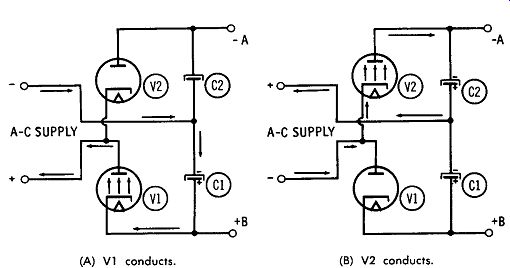
FIG. 5. Operation of voltage-doubler rectifier.
(A) V1 conducts. (B) V2 conducts.
THE VOLTAGE MULTIPLIER
The voltage multiplier represents another basic type of power supply configuration. It can provide an output voltage greater than the applied voltage without the use of a step-up transformer.
FIG. 5 shows one form of voltage multiplier known as a voltage doubler. During one half-cycle of the applied a-c input, the plate of V1 is positive with respect to the cathode. Electrons then flow through V1, charging C1 to the polarity shown.
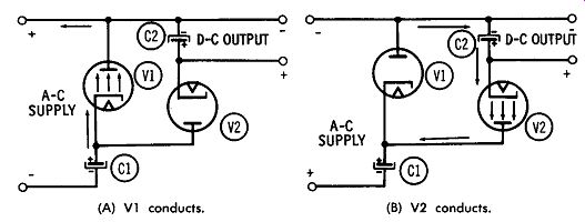
FIG. 6. Modified voltage doubler. (A) V1 conducts. (B) V2 conducts.
On the following half-cycle ( FIG. 5B), the plate of V2 is positive with respect to the cathode, and electrons flow through V2, charging C2. Since the voltages across C1 and C2 are in series, the voltage at the output terminals (points A and B) is the sum of the individual voltages across each capacitor.
FIG. 6 shows another voltage-doubler arrangement. During the a-c input when the plate of V1 is positive with respect to the cathode, V1 conducts, charging C1. On the following half-cycle, the voltage on C1 adds to the supply voltage so twice the supply voltage is applied to V2 and C2. Since its plate is now positive, V2 conducts and C2 charges. Thus, the d-c output is approximately twice the value of the a-c input.
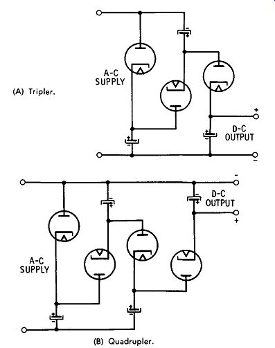
FIG. 7A is the circuit of a voltage tripler, and FIG. 7B is the circuit
of a voltage quadrupler. Their basic operation is the same as that of
the voltage multiplier shown in FIG. 6, except for the use of additional
rectifiers and capacitors.
FIG. 7. Voltage-multiplier circuits.
(A) Tripler.
(B) Quadruple,.
COMPARISON OF THE BASIC RECTIFIER SYSTEMS
Each of the four basic types of power-supply rectifier configurations has its merits and disadvantages. The half-wave rectifier is used primarily where only a relatively modest d-c output current is required up to about 50 ma. It is generally not used to deliver higher currents because of its inefficiency and because of the difficulty in filtering (smoothing out) its pulsating output.
The full-wave rectifier is the most common of all power-supply con figurations. It is more efficient, and its output is more easily filtered than that of the half-wave rectifier. The full-wave rectifier does, however, require a center-tapped transformer winding to supply its operating power, and this can be a disadvantage in some applications.
The bridge rectifier is on a par with the full-wave rectifier in regard to efficiency and ease of filtering the output; it has the advantage of not requiring a center-tapped transformer. On the other hand, the bridge rectifier requires four rectifier diodes, whereas the full-wave rectifier requires only two. The bridge rectifier has become increasingly popular with the development of semiconductor diodes.
Voltage-multiplier circuits are chiefly used where the d-c_ output voltage must be higher than the a-c supply voltage, but where the use of a voltage step-up transformer is not desirable. Voltage-multiplier circuits are used typically on portable tv receivers, electronic photo flash units, etc.
TYPES OF RECTIFIERS
Rectifiers come in a wide variety of sizes, shapes, and methods of construction. Among the first to be developed were the vacuum tubes which featured large glass bulbs. Refinements in manufacturing techniques soon reduced the size and increased the current-carrying capabilities. Gas-filled tubes were developed to fill the need for more powerful units. Although these were used in industrial and commercial applications for the most part, some found places in portable radios, car radios, etc. The cold-cathode tubes resulted from efforts to limit the power lost in tube heaters and filaments.
The introduction of semiconductor rectifiers has created an entirely new field. They are rapidly replacing tubes in many of the conventional rectifier circuits. Their small size makes them particularly attractive in miniaturized equipment.
High-Vacuum Rectifiers
One of the most common rectifiers is the high-vacuum rectifier shown in FIG. 8. The half-wave high-vacuum diode rectifier ( FIG. 8A) consists of a single cylinder-shaped plate that surrounds a heated cathode. The cathode may be either directly or indirectly heated. The directly heated cathode is simply a wire coated with a metallic oxide that emits electrons when heated. The indirectly heated cathode consists of a "cathode sleeve" upon which is deposited an electron-emitting metallic oxide. The sleeve is raised to the proper operating temperature by a coil of heater wire placed inside the cathode and electrically insulated from it. The wire is heated by passing current through it. Half-wave high-vacuum diodes are primarily used as damper diodes (in tv receivers) and as high-voltage rectifiers (in tv receivers and specialized industrial equipment). The full-wave high-vacuum diode ( FIG. 8C) is designed especially for use in full-wave rectifier circuits. It consists of two individual plates, each surrounding a heated cathode. The two cathodes are electrically connected in parallel. Like half-wave diodes, full-wave diodes may use either a directly or an indirectly heated cathode, the former being more common.
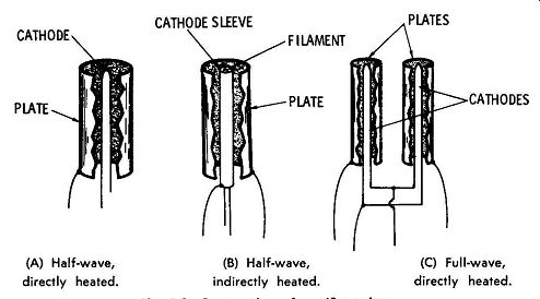
FIG. 8. Construction of rectifier tubes.
(A) Half-wave, directly heated.
(B) Half-wave, indirectly heated.
(C) Full-wave, directly heated.
-------- A full-wave high-vacuum rectifier tube designed for heavy
duty in industrial and commercial equipment. Courtesy RCA.
Mercury-Vapor Diodes
High-vacuum diodes are limited to output currents of about 300 maximum. Higher current outputs than this from vacuum diodes re-quire tubes of excessive size if satisfactory efficiency is to be maintained.
The mercury-vapor rectifier diode has a much higher current capacity because of the introduction of a small amount of mercury into its envelope. As the cathode is heated, a portion of the mercury vaporizes, filling the envelope with vapor. The mercury vapor greatly reduces the internal resistance of the diode, so that the tube can carry large values of current with only a small voltage drop.
FIG. 9 shows how the introduction of mercury vapor reduces the cathode-to-plate voltage drop. When the plate is positive with respect to the cathode, it attracts some of the electrons emitted by the cathode.
Other electrons remain near the cathode, forming what is known as a space charge; this tends to limit the electron flow to the plate. The electrons traveling toward the plate encounter the mercury-gas atoms.
When they collide, electrons are knocked loose from the mercury atoms. The mercury atoms that have thus lost electrons become positive ions. The positive ions neutralize some of the space-charge electrons which surround the heated cathode, so more electrons are able to move toward the plate. As they do, they strike additional gas molecules, producing additional ions. This process "snowballs," producing a large flow of electrons between cathode and plate.
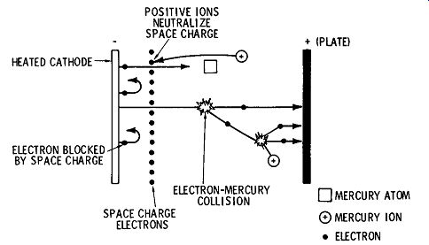
FIG. 9. Operation of mercury-vapor rectifier.
Cold-Cathode Gas Rectifiers
The cold-cathode gas rectifier is similar to the mercury-vapor rectifier just described in that a gas is placed in the envelope to reduce internal resistance. The major difference between the two, however, is that the cold-cathode rectifier does not contain a heated cathode. Its operation is made possible by an internal construction which enables ionization to take place without the need for a heated cathode.
Cold-cathode gas diodes at one time were popular in portable and automotive electronic equipment where only a limited amount of power was available. The saving resulting from the elimination of heater current was an advantage. They have since been almost entirely replaced by semiconductor rectifiers.
Semiconductor Rectifiers
Semiconductor rectifiers, because of their small size, ruggedness, and low voltage drop, are rapidly replacing high-vacuum and gas-filled rectifier diodes in a large number of applications. There are four major types of semiconductor rectifiers-copper oxide, selenium, germanium, and silicon. The copper-oxide rectifier is the oldest type.
However, it has been almost entirely replaced by selenium, germanium, and silicon rectifiers so it is of historic interest only.
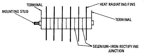
FIG. 10. Construction of selenium rectifier (half-wave).
FIG. 10 shows the physical construction of the selenium rectifier.
The actual process of rectification takes place at the junction of a thin film of metallic selenium with an iron surface. Although selenium rectifiers offer advantages of size and ruggedness when compared to high-vacuum and gas-filled rectifiers, they have the disadvantage of allowing a small amount of current in the reverse direction (when the anode is negative with respect to the cathode). This lowers their operating efficiency.
The amount of current a rectifier passes in the reverse direction compared to the amount it passes in the normal ( or forward) direction determines the forward-to-reverse current ratio of a rectifier. Vacuum and gas rectifiers have a very high forward-to-reverse current ratio because they conduct essentially zero current in the reverse direction.
Semiconductor rectifiers do allow some reverse current, so they have a smaller forward-to-reverse current ratio. However, the small amount of reverse current in the selenium rectifier is of little importance in most circuits, and the small size and ruggedness of selenium rectifiers make them useful in many applications.
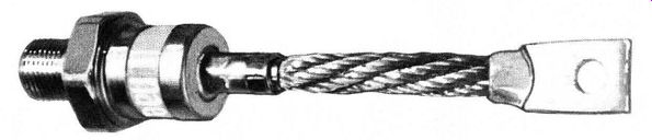
Germanium-diode rectifiers have a much greater forward-to-reverse current ratio than selenium rectifiers. They can handle larger currents, because the ability to dissipate power in the form of heat is not wasted by reverse current in the rectifier. Also, germanium rectifiers have a very low forward-current impedance which further adds to their power-handling capability. The chief factor limiting the power which germanium-diode rectifiers can handle is their maximum operating temperature. When this is exceeded, the rectifier is destroyed.
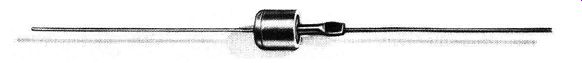
Courtesy Electronic Devices, Inc.
A small silicon rectifier capable of handling 2 amperes, available with a PIV of 20 to 1000 volts, in an axial lead case.
Silicon-diode rectifiers are basically similar in characteristics to germanium rectifiers. However, silicon diodes can withstand a much higher operating temperature and thus can handle greater amounts of power.
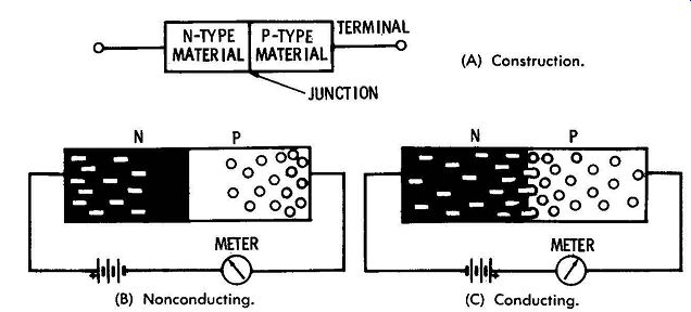
FIG. 11. Operation of silicon junction diode. (A) Construction. (B)
Nonconducting. (C) Conducting.
FIG. 11 shows the basic construction of a silicon-diode rectifier.
(The operation of the germanium rectifier is essentially the same.) A silicon diode consists of a piece of N-type and a piece of P-type semi conductor fused together.
Courtesy International Resistance Co. A 250-ampere silicon rectifier in
a D0-9 case.
The composition of the N-type material is such that there are a large number of molecules with loosely bonded electrons that are available for carrying current. The P-type material is just the opposite. The molecules of material there are capable of accepting additional electrons, so it is said that "holes" exist in their structure. The electrons in N-type material are called negative-charge carriers, and the holes in P-type material are called positive-charge carriers.
When the two materials are fused together a junction is formed that conducts current readily in one direction but not in the other. If a voltage is applied so the P-type is positive and the N-type is negative, there is current in the circuit. When the voltage reverses, there is no current.
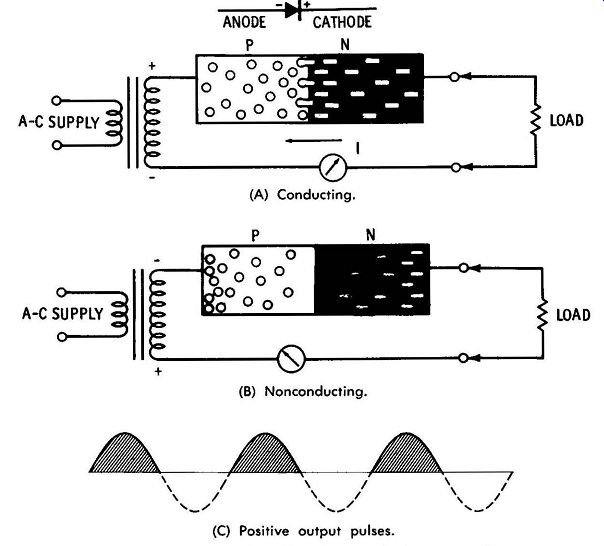
FIG. 12. Operation of a silicon junction diode as rectifier. (A) Conducting.
(B) Nonconducting. (C) Positive output pulses.
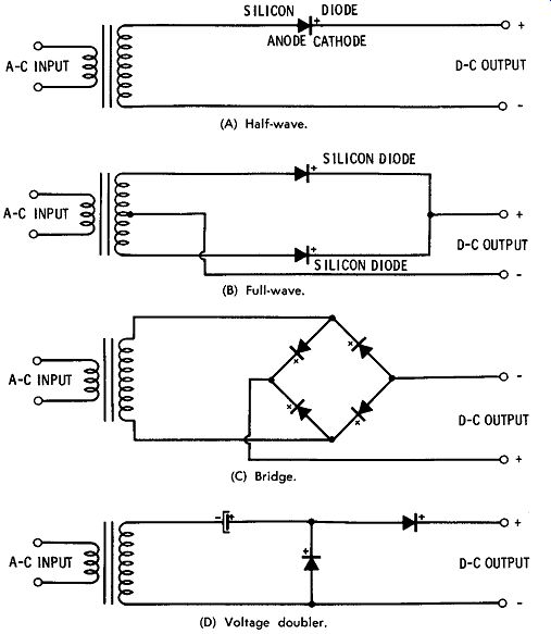
FIG. 13. Silicon-diode
rectifier configurations. (A) Half-wave. (B) Full-wave. (C) Bridge.
(D) Voltage doubler.
FIG. 11B shows the silicon diode connected into a circuit containing a battery and an indicating meter. The negative terminal of the battery is connected to the P-type material, and the positive battery terminal is connected to the N-type material (through the meter). Negative-charge carriers (electrons) are attracted to the positive battery terminal, thus moving away from the junction. The positive charge carriers (holes) are attracted to the negative battery terminal, and thus also move away from the junction. Since there are no charge carriers at the junction, there is no current in the circuit, as indicated by the meter. In a semiconductor diode, current is provided by the flow of charge carriers, either electrons or holes, across the junction.
In FIG. 11C, the battery connections are reversed so that the positive battery terminal is connected to the P-type semiconductor, and the negative battery terminal is connected to the N-type semiconductor. The negative charge carriers are repelled away from the negative battery terminal, toward the junction of the N- and P-type semiconductors. Likewise, the positive charge carriers are repelled away from the positive battery terminal, toward the junction. The positive and negative charge carriers combine at the junction, resulting in current across the P-N junction. Current in the circuit is indicated by the meter.
FIG. 12 shows a silicon diode connected in a simple half-wave rectifier circuit. In FIG. 12A, the first half-cycle of the a-c input is applied so the P-type material is positive and the N-type material is negative. Under these conditions, the positive-charge carriers (holes) in the P-type semiconductor are repelled toward the P-N junction, and the negative-charge carriers (electrons) are likewise repelled toward the P-N junction. Electrons and holes combine at the P-N junction, and current in the circuit is indicated by the meter.
In FIG. 12B, the second half-cycle of the a-c input is applied so the P-type material is negative. Negative-charge carriers (electrons) are attracted away from the P-N junction, as are the positive-charge carriers. As a result, there is no charge-carrier combination at the junction, and no current is indicated by the meter. The resulting current pulses through the load are shown in FIG. 12C. FIG. 13 shows how silicon-rectifier diodes may be used in half wave, full-wave, bridge, and voltage-multiplier rectifier circuits.
Also see: