AMAZON multi-meters discounts AMAZON oscilloscope discounts
Earlier in this guide you learned the basics of electron flow. You discovered that electrical current is actually a flow of negative charge carriers called electrons . Electrons orbit around the nucleus of an atom, just as the earth orbits around the sun. Electrons are held in their orbital paths by their attraction to the positive nucleus, which contains the positive charge carriers called protons. Electrons are attracted to the positive nucleus because of a basic law of physics which states "unlike charges attract, and like charges repel." This same principle can be demonstrated by observing the attraction between two permanent magnets. The two north poles of the magnets will repel each other, but a north pole and south pole will attract. In the same way, the unlike charges of the negative electron and the positive proton attract one another.
Introduction to Solid-State Devices
Because one electron (negative-charge carrier) will equalize the effect of one proton (positive-charge carrier), a normal atom will be balanced in reference to the number of electrons and protons it contains. For example, if an atom has 11 electrons, it will also contain 11 protons. The end result is the negative charge of the electrons will be canceled out by the positive charge of the protons, and the atom will not present any external charge.
The orbital paths of the electrons around the nucleus follow a definite pattern of circular shells or rings. The maximum number of electrons in each shell is defined by the formula 2(n2 )where n = shell number
For example, if you wanted to calculate the maximum number of electrons for the first shell, n would be 1:
2(1 x 1) = 2
The maximum number of electrons in the first shell of any atom is 2, regardless of the total number of electrons in that particular atom. Similarly, the maximum number of electrons in the second shell is
2(2 + 2) = 8
The maximum number of electrons in the second shell of any atom is 8.
This goes on and on, with the maximum number of electrons in the third, fourth, and fifth shells as 18, 32, and 50, respectively.
In electronics, only the outermost shell of an atom is important because all electron flow occurs with electrons from this shell. The outermost shell of any atom is called the valence shell. If the atomic structure of any substance is made up of atoms containing the maximum number of electrons in their valence shells, the substance is said to be an insulator because the electrons are rigidly bonded together. If a substance is made up of atoms with valence shells far from being full, the electrons are easily loosened from their orbital bonds, and the substance is said to be a conductor. The principle can be compared to buying a new bottle of aspirin. In the beginning, when the aspirin bottle is full, you can shake the bottle, but produce very little movement of the pills because they are tightly packed together. But when you have only a few pills left in the bottle, even the slightest movement will produce a chorus of rattling and rolling pills. Think of this illustration the next time that the electrical-electronics field gives you a headache! The atoms in some types of crystalline substances (such as silicon) fill their valence shells by overlapping the orbital paths of neighboring atoms.
An isolated silicon atom contains four electrons in its valence shell. When silicon atoms combine to form a solid crystal, each atom positions itself between four other silicon atoms in such a way that the valence shells over lap from one atom to another. This causes each individual valence electron to be shared by two atoms. By sharing the electrons from four other atoms, each individual silicon atom appears to have eight electrons in its valence shell. This condition of sharing valence electrons is called covalent bonding.
In its pure state, silicon is an insulator because the covalent bonding rigidly holds all of the electrons leaving no (easily loosened) free electrons to conduct electrical current. If an impurity is injected into the pure sil icon, having a valence shell containing five electrons, it cannot fit into the covalent bonding pattern of the silicon. The result is one free electron per impurity atom that can readily move and conduct current.
Similarly, if an impurity is injected containing only three electrons in its valence shell, the absence of the fourth electron (needed for proper covalent bonding) causes a free positive charge. (A free positive charge is another way of describing a hole, or the absence of an electron.) In both cases, a semiconductor has been formed. The term semiconductor simply indicates the substance is neither a good insulator nor a good conductor; it is somewhere in between. (The term "semi-insulator" would be just as accurate as the term semiconductor.) The process of injecting an impurity into a substance to form a semiconductor is called doping.
In addition to becoming a semiconductor, the impure silicon will also possess a unique property, depending on whether it has been doped with a pentavalent impurity (an impurity with five electrons in its valence shell), or with a trivalent impurity (an impurity with three electrons in its valence shell). Silicon doped with a pentavalent impurity will become N-type material, and it will contain an excess of negative charge carriers (one free electron per impurity atom). Silicon doped with a trivalent impurity will become P-type material, and it will contain an excess of positive charge carriers (one "hole" per impurity atom).
Diode Principles
When N-type semiconductor material is sandwiched with P-type material, the resulting component is called a diode, which is a two-layer device that has an extremely low resistance to current flow in one direction, and an extremely high resistance to current flow in the other. Because it is a two-layer device, it can also be considered a single-junction device because there is only one junction between the P and N material, as shown in Fig. 1. A diode is often called a rectifier.
Ideally, you can consider a diode as being capable of passing current in only one direction. If the P-side voltage is positive, relative to the N side, by an amount greater than its forward threshold voltage (about 0.7 volt if silicon, and 0.3 volt if germanium), the diode will freely pass current almost like a closed switch. This diode is said to be forward-biased. If the P side is negative, relative to the N side, virtually no current will be allowed to flow, unless and until the device's breakdown voltage is reached. This condition is referred to as being reverse-biased. If the reverse breakdown voltage is exceeded (the point at which reverse-biased current starts to flow) in most normal diodes, the diode may be destroyed.
The P side of a diode is called the anode. The N side is called the cathode (Fig. 2).
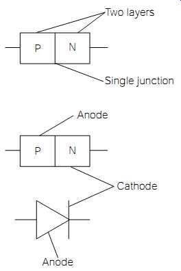
FIG. 1 Basic diode construction.
FIG. 2 Diode labels and electrical symbol.
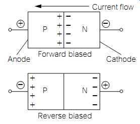
FIG. 3 Diode operational principles.
The principle behind diode operation is shown in Fig. 3. The diagram of a forward-biased diode demonstrates the operation of a diode in the for ward conduction mode (freely passing current). With the polarity, or bias, of the voltages shown, the forward-biased diode will conduct current as if it were a closed switch. As stated previously, like charges repel each other. If a positive voltage is applied to the P material, the free positive-charge carriers will be repelled and move away from the positive potential toward the junction.
Similarly, the negative potential applied to the N material will cause the free negative-charge carriers to move away from the negative potential toward the junction. When the positive- and negative-charge carriers arrive at the junction, they will attract (unlike charges attract) and combine. As the positive- and negative-charge carriers combine at the junction, a new positive- and negative-charge carrier will be introduced to the semiconductor material from the source voltage providing the bias.
As these new charge carriers enter the semiconductor material, they will move toward the junction and combine. Thus, current flow is established, and will continue for as long as the bias voltage remains above the forward-bias threshold.
The forward-threshold voltage must be exceeded before a forward-biased diode will conduct. The forward-threshold voltage must be high enough to loosen the charge carriers from their atomic orbit and push them through the junction barrier. With silicon diodes, this forward-threshold voltage is approximately 0.7 volt. With germanium diode s , the forward threshold voltage is approximately 0.3 to 0.4 volt.
The maximum forward current rating of a diode is based on its physical size and construction. Diode manufacturers will typically specify this rating in two ways: the "maximum continuous (or average) forward cur rent" and the "peak forward surge current." The maximum continuous for ward current is precisely what the name implies: the maximum forward current the diode can conduct on a constant basis. The peak forward surge current is the maximum forward current a diode can conduct for 8.3 milliseconds. This last specification can be between 5 and 50 times higher than the continuous rating. 8.3 milliseconds is used as a standard reference for this rating, because it is the time period for one half-cycle of 60 hertz AC. Diodes used for power rectification experience a surge current on the initial application of power (covered further in Section 5).
FIG. 3 also illustrates a diagram of a reverse-biased diode. As might be expected, the opposite effect occurs if the P material is negative biased, relative to the N material. In this case, the negative potential applied to the P material attracts the positive charge carriers, drawing them away from the junction. Similarly, the positive potential applied to the N material draws the negative charge carriers toward it, and away from the junction. This leaves the junction area depleted; virtually no charge carriers exist there. Therefore, the junction area becomes an insulator, and current flow is inhibited.
The reverse-bias potential might be increased to the reverse-breakdown voltage for which the particular diode is rated. As in the case of the maximum forward current rating, the reverse-breakdown voltage is specified by the manufacturer. The reverse-breakdown voltage is much higher than the forward threshold voltage. A typical general-purpose diode might be specified as having a forward-threshold voltage of 0.7 volt, and a reverse breakdown voltage of 400 volts. Exceeding the reverse-breakdown voltage is destructive to a general-purpose diode. [Some manufacturers refer to the reverse-breakdown voltage as the peak inverse voltage (PIV) or as the peak reverse voltage (PRV).] Diodes are commonly used to convert alternating current (AC) to direct current (DC). This process is called rectification. A single diode used for rectification is called a half-wave rectifier. When four diodes are connected together, and are used to redirect both the positive and negative alternations of AC to DC, the four diode configuration is called a diode bridge, or a bridge rectifier. These configurations can be demonstrated in a few common types of circuits.
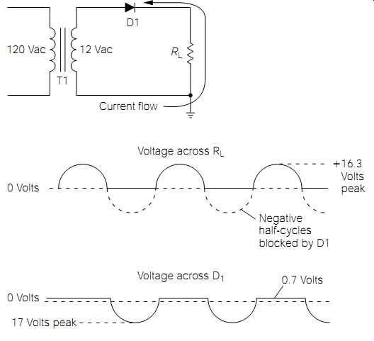
FIG. 4 Half-wave rectifier circuit.
FIG. 5 Waveshapes across D1 and RL from circuit illustrated in Fig. 4.
FIG. 4 shows a simple half-wave rectifier circuit. Common house hold power (120 volts AC rms) is applied to the primary of a step-down transformer (T1). The secondary of T1 steps down the 120 volts AC rms to 12 volts AC rms. The diode (D1) will only allow current to flow in the direction shown (from cathode to anode). Diode D1 will be forward biased during each positive half-cycle (relative to common). When the circuit current tries to flow in the opposite direction, the diode will be reverse-biased (positive on the cathode, negative on the anode), causing the diode to act like an open switch. As shown in Fig. 5, this results in a pulsating DC voltage applied across the load resistor (Rload ). Because common household power cycles at a 60-hertz frequency, the pulses seen across Rload will also be at 60 hertz. FIG. 5 also shows the voltage waveform across D1.
During the positive half-cycle, D1 will drop the 0.7 volt forward threshold voltage. Rload will drop the majority of the voltage, about 11.3 volts in this case. The term drop refers to the fact that a certain voltage difference appears across an electrical device, or component, as a current flows through it. In this example, 0.7 + 11.3 = 12 volts DC total. The entire negative half-cycle will be dropped across D1 while it is reverse biased. The negative half-cycle is dropped across D1 because it looks like an open switch when reverse-biased. An open switch is an infinitely high resistance. Note that D1 is in series with Rload. As discussed previously, in a series circuit, the higher the resistance value of a component, the more of the source voltage it will drop. Because D1 looks like an infinitely high resistance when reverse-biased, it will drop the total source voltage (output of T1's secondary) during the negative half-cycle.
Consider the amplitude of the voltage developed across Rload. As shown in Fig. 4, the secondary of T1 is 12 volts AC rms (AC voltages are always assumed to be V rms values unless otherwise stated). Therefore, the peak voltage output from the T1 secondary is:
Peak _ (rms value )1.414 _ (12 volts AC) 1.414 _ 16.968 volts peak
For discussion purposes, the 16.968 volts can be rounded off to 17 volts.
The previous calculation tells us that for each full cycle, the T1 secondary will output one positive 17-volt peak half-cycle, and one negative 17 volt peak half-cycle. The negative half-cycles are blocked by D1, allowing Rload to receive only the positive half-cycles. The actual peak voltage across Rload will be the 17-volt positive peak, minus the 0.7-volt forward threshold voltage being dropped by D1. In other words, 16.3-volt positive peaks will be applied to Rload , as shown in Fig. 5.
The diode circuit illustrated in Fig. 4 is called a half-wave rectifier, because only one-half of the full AC cycle is actually applied to the load. However, it would be much more desirable to utilize the full AC cycle. The circuits shown in Fig. 6 are designed to accomplish this, and they are called full-wave rectifiers.
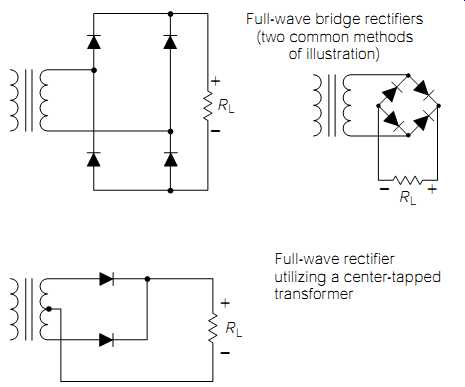
FIG. 6 Two types of full-wave rectifiers.
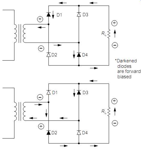
FIG. 7 Current flow through a full-wave bridge rectifier.
The full-wave bridge rectifier illustrated in Fig. 6 is the more common type of AC rectifier. It consists of four diodes. The operation of a full wave bridge rectifier can be examined by referring to Fig. 7. When the transformer secondary outputs a half-cycle with the polarity shown in the top illustration, the current will follow the path indicated by the arrows. (Remember, forward current always flows through a diode from cathode to anode.) With this polarity applied to the bridge, diodes D1 and D4 are forward-biased, while D2 and D3 are reverse-biased.
The lower illustration of Fig. 7 shows the current path when the polarity on the transformer secondary reverses. With this polarity applied to the bridge, diodes D2 and D3 are forward-biased, while D1 and D4 are reverse-biased. In either case, the current always flows through the load resistor, Rload , in the same direction; meaning that the voltage polarity across Rload does not change. Essentially, the switching action of the diode bridge actually turns the negative half-cycle upside down.
Referring back to the circuit of Fig. 4, and to its associated waveforms shown in Fig. 5, note that Rload receives the positive half-cycles only of the AC being output by T1's secondary. These positive half-cycles occur at a 60-hertz rate because the full AC cycle is at a 60-hertz rate. Compare this to the circuit of Fig. 7, and to its associated waveshapes shown in Fig. 9. Note how Rload will now receive the negative half-cycle turned upside down (converted to another positive half-cycle) as well as the regular positive pulse. In a sinusoidal waveform, the negative half-cycle is the exact inversion of the positive half-cycle; thus, the waveform across Rload will begin to repeat itself at the end of the first half-cycle. In simple terms, the frequency will double. The frequency of the transformer secondary is 60 hertz AC, but the frequency at the output of the diode bridge is 120-hertz pulsating DC.
You might be confused about the difference between AC and pulsating DC. As stated in the previous section, AC is characterized by a voltage polarity and current flow reversal. With pulsating DC, there is a large AC component, usually called ripple, but the current flow never changes direction through the load. Obviously, this means that the voltage polarity never changes either. In Fig. 9, note that the pulsating DC never crosses the zero reference line into the negative region.
The functional diagram of a full-wave rectifier, utilizing a transformer secondary with a center tap, is illustrated in Fig. 8. This functions just as well as the bridge rectifier discussed previously, and all of the wave shapes shown in Fig. 9 are applicable to this circuit as well. The secondary center tap becomes the circuit common (or circuit reference). As shown in Fig. 10, the two outputs from each side of the secondary are exactly opposite to each other, in reference to the center tap (180 degrees out of phase). If one output is in the positive half-cycle, the other out put must be in the negative half-cycle and vice versa. Thus, during each half-cycle (of the applied AC to the primary), one of the two secondary outputs will output a positive half-cycle.
The circuit of Fig. 8 is actually two half-wave rectifiers connected to the same load. The two outputs from the transformer secondary are inverted (opposite) from each other. Therefore, if D1 is forward-biased, D2 will be reverse-biased. When D1 becomes reverse-biased, D2 becomes for ward-biased. The end result is that the inverted action of the two half wave rectifiers are combined to form one full-wave rectifier. The effect is the same as that achieved with the circuit of Fig. 7. However, to obtain the same DC voltage amplitude to the load, the transformer's rated secondary voltage, in Fig. 8, must be twice the value of the transformer shown in Fig. 7. This is because the center-tap will divide the voltage in half when it is used as the common, or reference. For example, a 24-volt, center-tapped transformer secondary will measure 12 volts rms from the center tap to either side of the secondary.
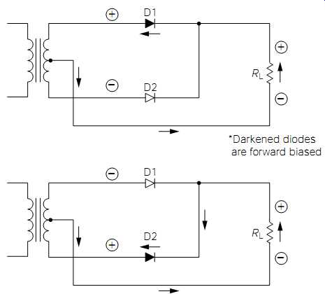
FIG. 8 Current flow through a center-tapped transformer full-wave rectifier.
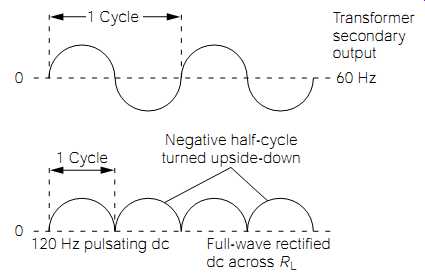
FIG. 9 Applied 60-hertz AC waveshape compared to the 120-hertz pulsating
DC output of a full-wave rectifier.
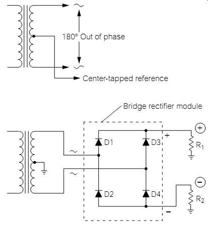
FIG. 10 Two leads of a center-tapped transformer 180 degrees out of
phase when ct is used as the reference.
FIG. 11 Dual-voltage rectification circuit.
A third common full-wave rectification circuit is illustrated in Fig. 11. This circuit is actually the same center-tapped full-wave rectifier circuit as shown in Fig. 8, but with two additional diodes incorporated. Referring to Fig. 8, the top diagram illustrates how the upper half of the secondary output is applied to Rload , while the lower half of the secondary output is blocked by D2. The reverse occurs in the lower diagram. In both cases, half of the secondary output is not used.
The circuit in Fig. 12 utilizes this unused portion of the secondary output to form another DC output of the opposite polarity. This can be more easily understood by referring back to Figs. 11 and 8. FIG. 12 is exactly the same circuit (with the same component labeling) as illustrated in Fig. 11. Compare Fig. 12 with Fig. 8. Notice how the positive full wave rectification section of Fig. 12 is identical to the circuit illustrated in Fig. 8. The circuit of Fig. 12 incorporates two additional diodes (D4 and D2) to form another full-wave output from the unused half-cycles.
Because of the orientation of the diodes, it will be negative in respect to the circuit common. Dual-polarity power supplies are very common because of their extensive use in operational amplifier and audio circuits; both of which will be discussed later in this guide. As in the case of the center tapped full-wave rectifier circuit of Fig. 8, the voltages across R1 and R2 will be only half of the amplitude of the secondary rating.
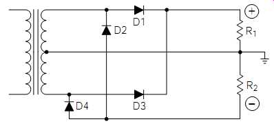
FIG. 12 Redrawn schematic of Fig. 11.
Referencing
By now, you might be beginning to appreciate the importance of wave shapes in the electrical and electronics fields. All of the waveshapes shown in the previous sections are shown just as they would appear if they were viewed with an oscilloscope. When discussing voltage wave shapes, they are always said to exist with respect to some point of "reference." As pointed out in Section 2, voltage readings are always taken in respect to some common point of reference.
To help in understanding this, consider the following analogy. If an airplane is said to be flying at an altitude of 10,000 feet, it is always assumed that the point of reference is sea level. If the point of reference was changed to a 5000-foot mountaintop, the plane would then be said to be flying at a 5000-foot altitude. If the plane were to be flying close to the ground, it could be said that it was flying at nearly a "negative" 5000-foot altitude.
Referring back to Fig. 10, the center tap essentially splits the trans former secondary into two halves when it is used as the common reference. In the same way that you could make the airplane fly at a negative altitude by moving the reference point up, you can provide an inverted output by moving the circuit reference up to the halfway point of the secondary output.
Unless otherwise stipulated, voltage amplitudes and waveshapes will always be in reference to the circuit common (usually the chassis "ground") on all schematics and electrical drawings.
Assembly and Testing of Second Section of a Lab Power Supply
The following materials are needed:
Quantity | Description
1 6-amp, 200-volt PIV bridge rectifier module
2 10-kohm, 1/2 -watt resistors
The type of bridge rectifier module specified is commonly available.
Although the case styles vary somewhat with different manufacturers, it should be a square or rectangular block, about an inch on each side, with a mounting hole in the middle. (There are some rectifiers with these ratings, meant for PC board installation; they do not have a hole in the middle, and they will be harder to mount.) The two 10-kohm resistors will be used for testing purposes only. Their tolerance rating, and other parameters, are not important.
Testing Bridge Rectifier Modules
Before mounting the bridge rectifier module, it is good practice to test its functional operation. This will help you understand it and provide you with more experience at using your DVM.
A DVM measures resistance by applying a low voltage to the unknown resistance value, measuring the current through the unknown resistance, and converting the current reading to a resistance reading. The older forms of DVMs, usually called vacuum-tube voltmeters (VTVMs), would apply about 1.5 volts to the unknown resistance value for measurement purposes. When checking resistance values on solid-state equipment, it is often undesirable to use 1.5 volts as a measurement standard, because this is above the forward threshold voltage of junction devices (diodes, transistors, etc.), causing them to "turn on," and to interact with the component being measured. Interaction of this sort will cause errors in resistance measurements. For this reason, most modern DVMs use only a few tenths of a volt as the measurement standard. When the need arises to check a semiconductor junction, the DVM must be set to the "diode test" position. In this position, the DVM will apply about 1.5 volts to the semiconductor junction under test. The black DVM test lead is of negative polarity, and the red lead is positive. (Be sure you have the DVM test leads plugged into the correct holes on the instrument; black to common.) When testing a diode, touch the black DVM test lead to the cathode (the "banded" side of the diode body), and the red lead to the anode.
This forward-biases the diode, and the resistance reading should be low [the actual resistance reading is irrelevant; when testing semiconductor junctions, you are concerned only with "high (or infinite)" versus "low" readings]. By reversing the DVM leads (red on cathode; black on anode), the diode is reverse-biased, and the resistance reading should be infinitely high.
Be aware that some volt-ohm-milli-ammeters (VOMs) are reverse-polarized for their resistance checks; the positive DC potential being on the black probe. In this instance, your readings will always be reversed. Test about a dozen common diodes (1N4001 or 1N4148/1N914). If they all test "good" only when the probes are reversed, then you have positive volts on your black probe.
The bridge rectifier module you obtained for this project actually contains our diodes connected in a bridge configuration, as shown in Fig. 11. Four individual diodes would function just as well. The four internal-module diodes can be tested with a DVM just as though they were four standard diodes.
The bridge rectifier module should have four connection terminals, or leads, extending from it. Each terminal, or lead, should have an identification symbol associated with it, on the case of the module. Two of the terminals will be marked with an "AC" or the symbol for a sine wave; these are the AC input terminals from the transformer. The other two terminals will be specified with polarity symbols ("+" or "-" ); these are the DC output terminals. FIG. 11 illustrates the actual external and internal connections associated with the bridge.
Referring to Fig. 11, if you wanted to test the internal diodes labeled D1 and D3, you would place the black (negative) DVM lead on the - terminal of the diode module, and the red (positive) DVM lead to either one of the AC terminals of the module. A low resistance reading would indicate either D1 or D3, respectively, was functioning correctly. You actually wouldn't know which one of the diodes you were testing because the module will not specify any difference in the AC terminals.
The issue is totally unimportant; if either one of the diodes is defective, the whole bridge module must be replaced.
Rather than detailing each individual diode measurement, Table 1 will make it easy for you to check any bridge rectifier module. Use this table, in conjunction with Fig. 11, to understand how the measurements will check each internal diode.
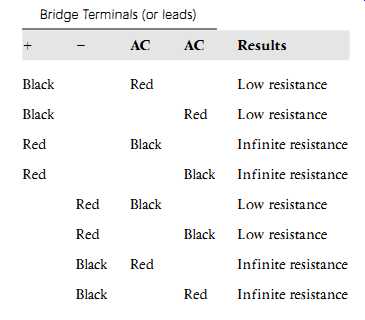
TABLE 1 Testing Bridge Diodes
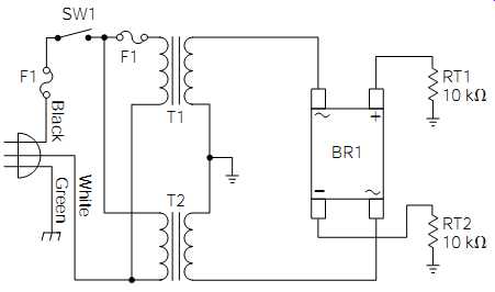
FIG. 13 Schematic diagram of the first and second sections of the lab
power supply.
Assuming that there were no problems with the bridge rectifier module, mount it close to the T1 and T2 secondaries, with the appropriate hardware. Wire and solder the connections from the T1 and T2 secondaries to the AC input terminals on the bridge module as illustrated in Fig. 13. Using an alligator clip lead, temporarily connect one side of test resistor RT1 to the positive terminal of the bridge rectifier. Connect the other side of RT1 to the circuit common connection between the two transformer secondaries with another clip lead. Using two more clip leads, connect one side of test resistor RT2 to the negative terminal of the bridge, and the other side to the same circuit common point as RT1.
Verify that your wiring is the same as is shown in Fig. 13. Be sure that all four clip leads are secure, and not touching anything except the desired connection point.
Turn off your lab outlet strip, and set SW1 to the "off" position. Plug the circuit into the outlet strip, and (using only one hand) turn on the outlet strip. Again, using only one hand, set SW1 to the "on" position. If F1 blows, turn off all power immediately; unplug the circuit; and double check all wiring. If the wiring is good, the fault must be in the bridge rectifier (assuming that you followed the test procedures for the first section of the power supply in the previous section).
Hopefully, F1 didn't blow, and you can leave the power applied to the circuit and continue with the test. Set your DVM to indicate "DC volts" on at least the 100-volt range. Use one more clip lead (and only one hand!) to connect the black DVM test lead to circuit common. Touch the red DVM test lead to the side of RT1 that is connected to the positive terminal of the bridge rectifier. You should read about 24 volts DC. Touch the red lead to the side of RT2 that is connected to the negative terminal of the bridge rectifier. You should read about -24 volts DC. Leave the black DVM test lead connected to the circuit common, and set the DVM to indicate "AC volts" on the same range. Again, measure the voltage across RT1 , and then RT2. Both readings should be about 12 volts AC.
Turn SW1 off, turn the outlet strip off, and unplug the circuit.
Referring back to Fig. 9, the DC voltage across RT1 and RT2 was pulsating DC as shown in the bottom waveform illustration. The DVM did not measure the peaks of the DC pulses; it read the effective DC level. You might think of it as "cutting off the peaks, and using that energy to fill in the valleys." The AC voltage across the resistors is called the AC component , or the ripple. The DVM measured the rms value of this AC component.
If you own an oscilloscope, read the owner's manual, and be sure you understand how to operate it correctly and safely. Then, use it, in con junction with this power supply circuit, to observe these waveforms.
They should appear just as shown in the various illustrations. Do not try to view the waveforms of the transformer primaries without using an isolation transformer.
Resistors RT1 and RT2 were used for testing purposes only. They can now be removed from the circuit, together with the alligator clip leads used to temporarily connect them.