AMAZON multi-meters discounts AMAZON oscilloscope discounts
Transistorized RF stages are found in automobile radios be cause of the low signal input required and the high noise level at which the receiver operates. These considerations apply to both AM and FM broadcast receivers and to mobile receivers used for two-way communications.
Ordinary portable transistor radios seldom need or use RF stages. The first receiver stage is the converter, the output of which is the IF signal.
The IF stages are, of course, single-frequency RF stages.
Usually tuned transformer circuits are used for coupling. In these transformers, the primary is usually tapped at a low-impedance point to match the impedance of the driving stage. The other four leads are the primary and secondary windings.
Neutralization is sometimes used for stability. Actually, neutralization can be considered as negative feedback. In most broadcast-band RF or IF stages, transistors are chosen because they require no neutralization.
THREE-BAND RF AMPLIFIER
Using a 2N370 transistor, this RF amplifier covers the broad cast, the 4.5-11.5 -mhz, and the 10.5-23 -mhz bands. Each band has a separate tuned antenna and tuned output tank circuit. Tapped autotransformer coils are used in all antenna circuits except the broadcast band, where the transformer is wound around a ferrite rod. T1 is the standard broadcast antenna coil; L2 and L1 are the 4.5- to 11.5 -mhz and 10.5- to 23 -mhz coils, respectively. Output to the mixer is from an interstage transformer (L5 for the standard broadcast band, L4 for the center band, and L3 for the high band). Gain is reduced by adding feedback resistor R3 to obtain stable operation. The tank circuits are tuned with individual gang capacitors on each band, with provision for individual slug tuning of the coils.
The RF transistor ( 2N370) is biased with voltage divider R1 C14-R2 in the base-emitter circuit.
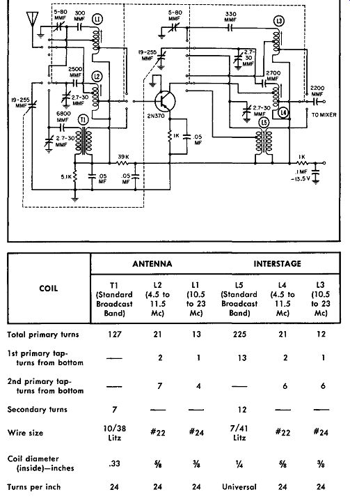
------------ Three-band RF amplifier. --- NOTE: Standard Broadcast Band
Antenna Coil ( T1) should be wound on an 8" x .33" ferrite rad.
WIDE-BAND VHF AMPLIFIER
This circuit shows a VHF ( 225-mhz) amplifier with a band width of 34 mhz and a gain of 33 db. Silicon mesa transistors ( Nl04B) are used in a common-base configuration. Although the circuit has less gain than the common-emitter type, its band width is greater and the circuit design is simpler at this frequency.
Short leads and good shielding are required for proper operation of this amplifier.
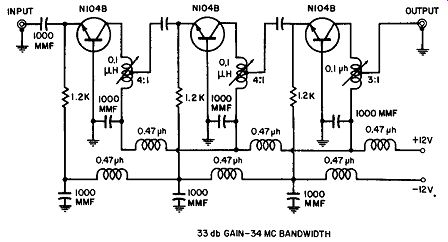
-------- Wide-band VHF amplifier.
50-mhz AMPLIFIER
This figure shows a 2Nl493 used as an RF amplifier operating at 50 me. It has a power output of 600 milliwatts ( 0.6 watt) and a gain of 10 db, with a collector voltage of 28 volts and a current of 23 mils. With an 8-db gain at 50 volts and 20 mils, an output of 1 watt can be obtained.
As shown, the circuit acts as a common-emitter amplifier--even though the collector is grounded--because the emitter and base are both isolated from ground. The potential of the entire trans former-secondary winding varies with the load voltage, and this potential difference drives the transistor.
The amplifier is biased well into Class C, depending on how much incoming signal is available. Increased drive permits more cutoff bias and thus a higher efficiency.
In operation, the transistor case should be firmly clamped to the chassis. This arrangement provides an adequate built-in heat sink. A 3" x 3" chassis is suitable for most environmental conditions at power levels of up to 1 watt.
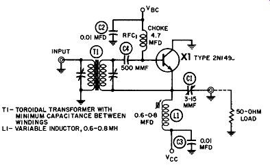
----------- 50-mhz amplifier.
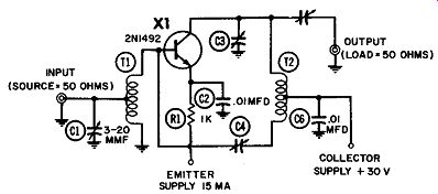
------------ 70 -mhz power amplifier.
70-mhz POWER AMPLIFIER
By using proper neutralization techniques, it is possible to de sign high-frequency transistor power amplifiers. This figure shows a 70-mhz power amplifier which can be used in intermediate or power-amplifier circuits to boost the output of either a low-level or a crystal oscillator.
This circuit has a power gain of 15 db at a collector voltage of 30 volts and a collector current of 15 ma. If a 2N1493 is used with the same supply voltages, power gain will be 12 db.
SELF-OSCILLATING MIXER (6 TO 26 Mhz)
This 2N1516 PNP germanium transistor is shown as a self-oscillating mixer. Conversion gain is 25 db at 6.5 mhz and 18 db at 26 me. ( Conversion gain is defined as the ratio between the IF power in a 2,500-ohm average load resistor connected across the output terminals of the IF filter, to the available HF power in the antenna circuit.) Self-oscillating mixer (6 to 26 mhz).
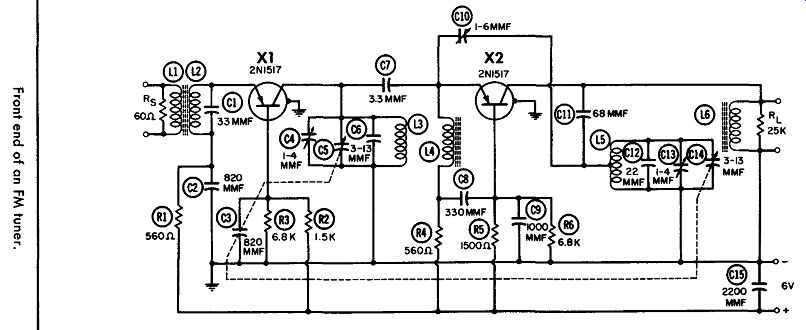
FRONT-END OF AN FM TUNER
This FM tuner consists of an RF amplifier and a self-oscillating mixer stage, each utilizing a 2Nl517 transistor. The total avail able power gain is 26 db average, 22 db minimum. The noise factor is less than 11 db ( 9 db average), and the image-rejection ratio is 22: 1.
The circuit is designed for use with a 6-volt battery. Shift of the oscillator frequency ( as a function of the battery voltage) is about 50 khz from 6 to 5 volts and about 100 khz from 5 to 4 volts.
At large input signals, the amplification of the RF stage must be reduced (e.g., by reducing the collector current of the stage) to avoid overloading the mixer stage.
The RF transistor operates at a collector current of 1.4 ma, and the mixer has a collector current of 1.5 ma. The tuner is designed for a frequency range of 87 to 101 me.
For optimum performance, adjustment of the oscillator voltage is recommended. At a battery voltage of 4 volts, the oscillator signal at the emitter should be adjusted to 80 millivolts by means of capacitor C10.
----------------
455-khz IF AMPLIFIER AND DETECTOR
This figure shows a single-stage 455 -khz IF amplifier using an MADT transistor. A 6-volt DC, one-mil supply is required. The maximum power gain is 55 db, but the maximum useful unneutralized power gain is only 44 db.
A diode detector ( 1N60A) provides audio across the 10K volume control.
DC SUPPLY VOLTAGE Vee ....................... -6 V
DC EMITTER CURRENTI E.. . . . . . . . . . . . . . .. . . . . .. 1 MA
MAXIMUM POWER GAIN .... . .................... 5 5 db
USEFUL UNNEUTRALIZED POWER GAIN ..... 44db
INPUT RESISTANCE . .. . ........ . . .............. 1200..n.
OUTPUT RESISTANCE ...... • 5M
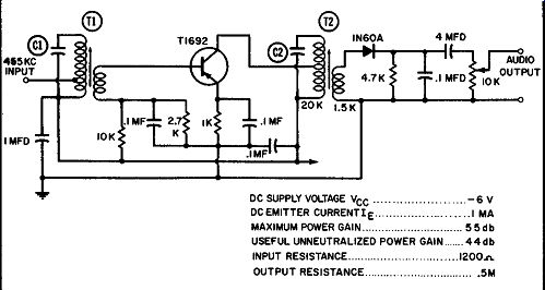
---------- 455 -khz IF amplifier and detector.
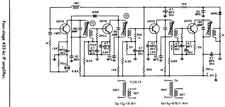
FOUR-STAGE 455-khz IF AMPLIFIER
A four-stage 455-khz IF amplifier using 2N715 silicon transistors is shown in Part A of the diagram. A 300-ohm load across the secondary of the transformers compensates for temperature changes.
Gain and bandwidth can be seen from Part B. AGC is obtained by adding a diode detector and an audio de coupling filter in the output of the IF strip. The detector diode produces a negative-going DC voltage, and an increased signal input tends to bias off the first stage. A diode is also used between the first and second stages to prevent overload.
Stage bias is such that a reverse voltage is developed across the diode detector under no-signal and low-signal conditions. As the signal level increases, the first stage draws a low enough cur rent that the diode can conduct. The forward impedance of the diode is now placed from the collector of the second stage to AC ground. Thus, the over-all IF gain is reduced.
--------------
43-mhz IF AMPLIFIER
This circuit shows a 2N623 used as a 43 -mhz IF amplifier operating from a -12-volt supply. Power output is 20 milliwatts with an 11-mhz bandwidth. Noise figure is 6 db, with a power gain of 15 db.
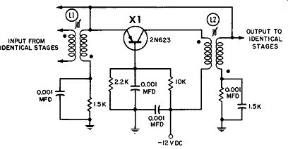
-------------- 43-mhz IF amplifier. L1, L2-Primary: 21T #30
-Secondary: 2¾ T #30
•secondary wound over bottom end of primary-¼ dia. form
--------- (A) Single stage.
------------------ (B)
60-mhz IF AMPLIFIER
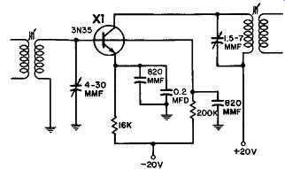
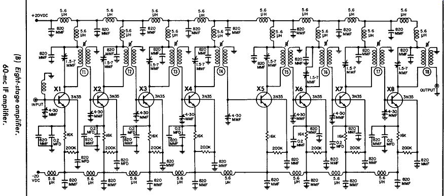
Here a 60-mhz IF amplifier using 3N55 tetrode silicon transistors is shown. This amplifier requires no neutralization and has a bandwidth of 20 me. The coupling transformers have a primary inductance of 1.365 µ-h and a secondary inductance of 0,2475 µ-h.
The coefficient of coupling is 0.43. Part A of the diagram shows a single stage of the eight-stage amplifier. All stages are identical except for the input and output, the transformers of which may be designed for the appropriate driving and load resistances.
In Part B, a two-battery supply is used to obtain a symmetrical circuit arrangement. Each transistor is biased common-base even though the RF circuitry is common-emitter. The large resistors in the emitter and base-2 leads keep currents constant in these elements. These resistors are bypassed for signal frequencies by appropriate capacitors. An additional 0.2-mfd capacitor helps in sure that the bias point will remain constant during a pulsed input signal. Decoupling is accomplished by the chokes and by pass capacitors shown in the complete amplifier schematic.
10.7-mhz IF AMPLIFIER
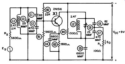
The schematic here shows a single 2Nl516 stage of a four-stage IF amplifier. The amplifier is operating at 10.7 me. The load of the stage ( input resistance of the following transistor) is 100 ohms, and the source resistance ( output resistance of the pre ceding transistor) is 5,600 ohms.
Instead of the last band filter, a discriminator filter with a selectivity of 1.5 can be used. ( The selectivity of the total amplifier at ±300 khz off-frequency is about 100.) The ratio of power out put to power input is 22 db. This figure includes the insertion losses of both tuned circuits ( 3.8 db each).
----------- 10.7-mhz IF amplifier.