AMAZON multi-meters discounts AMAZON oscilloscope discounts
Almost every form of electronic circuit must be operated from a power source such as a battery or an AC supply. Since the ad vent of semiconductors, power supplies ( and their associated regulating circuits) have taken on radical new designs and features. This section presents a wide variety of these newer transistor circuits.
Transistors are well suited for use in power supplies, since they provide varying amounts of power dissipation. This is possible because the transistor ( having a low internal IR drop) acts as a variable resistor in the circuit. By effective amplification of the circuit capacitance, the transistor can also be made to act as an excellent ripple filter.
Zener diodes, which in many ways resemble a gas-tube regulator, are often applied to circuits where a voltage reference is required. In most regulated power supplies, a fixed voltage is used as a reference, to establish an operating point for the power supply circuits.
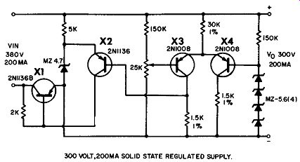
--------------- 300 VOLT,200MA SOLID STATE REGULATED SUPPLY. 300-volt
regulated supply.
300-VOLT REGULATED SUPPLY
Zener diodes, along with a transistor having an 80-volt collector-to-emitter bias and 16 watts' dissipation, can be used in the 300-volt range of power supplies. In this diagram, the transistor is in series with the negative lead of the regulated supply, while the series diodes are in parallel across the supply. The difference between the output and input voltage is 80 volts under minimum load conditions. At a maximum power-supply rating of 200 ma, the transistor dissipates approximately 16 watts.
In operation, an increase in load current will cause the parallel combination of X3 and X4 to conduct more heavily. X2 will then be biased more positive and cause the bias of X1 to also rise.
As a result, the output voltage will return to its nominal value.
A decrease in load current will reverse this action. Therefore, the output voltage of the power supply will be regulated to the particular voltage level required.
LOW-VOLTAGE POWER SUPPLIES
Here are four typical low-voltage power supplies that can be used with either audio amplifiers or test equipment.
Part A of the diagram shows a bridge of four 1N1692 silicon rectifiers with a single 1,500-mfd filter capacitor across them.
With a transformer secondary voltage of 25.2 volts AC, the power-supply output at no-load is -40 volts, and the output at 400 mils is - 33 volts. This supply can be used to power up to a 7-watt amplifier.
Part B of the diagram shows a supply that can be used to power two 7-watt audio amplifiers. With a secondary voltage of 24 volts AC, the no-load voltage is -38 volts; and with a 400 m-ohm load, the voltage drops to - 34 volts.
Part C of the diagram uses the same rectifiers across a 33-volt secondary. Here, the load is split into two parts by bringing the bleeder tap to ground and doubling the filters in capacity. Each output is - 50 volts at no-load and - 45 volts at 400 mils. This power supply can be used for two separate audio amplifiers of 10 watts each.
In D of the diagram, a 12-volt, 1-ampere supply is shown.
There are two -12-volt outputs. The one across the 12-volt zener diode is for a low-current load while the other-through the regulating power transistor-is for a high-current load.
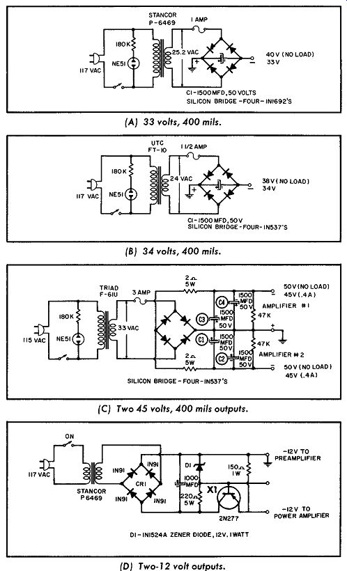
--------------- (A) 33 volts, 400 mils.
(B) 34 volts, 400 mils.
(C) Two 45 volts, 400 mils outputs.
(D) Two-12 volt outputs.
Low voltage supplies.
DC SUPPLY PHASE CONTROL
This figure shows a pair of SCR's in a single-phase power-control circuit in which control R7 permits adjustment of the output voltage from zero to maximum. The single UJT ( X1) is used to develop a gate signal to fire both SCR's on alternate half-cycles.
Through the rectifying action of CR1 and CR2-and the clipping action of CR3 and R1-a square-wave voltage with an amplitude of 20 volts is applied to UJT XL This voltage causes X1 to operate as a relaxation oscillator, and deliver a pulse of gate current to the SCR' s at a firing angle determined by the time constant of R6, R7, and Cl. The SCR which has a positive anode voltage during the gate pulse is the one that will fire, thus applying voltage to the load for that half-cycle.
When X1 reverses its degree of oscillation, the other SCR will fire, thus maintaining the output voltage constant. The firing angle can be adjusted by means of R7. At 60 hz, the firing angle of this circuit can be varied from approximately 10° to 180° ( fully off).
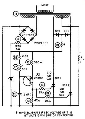
------------- DC supply phase control.
ZENER-CONTROLLED HIGH-CURRENT REGULATOR
A high-current power-supply design depends on the needs of the load. The unregulated source must be able to deliver between three and six volts more than the required output under full-load conditions. Also, the current dissipation of the transistors must be taken into consideration in the design of a power supply.
The circuit in this diagram consists of two cascade current amplifiers controlling four parallel-connected current transistors.
Since the output requirement of this power supply is high, the cascaded transistors act as a current amplifier to increase the power rating to 25 watts.
For higher-current applications, several parallel-connected transistors should be used as the current-passing element. As shown here, the four 2Nll36 transistors will easily handle 150 watts; and with ideal heat-sink conditions, they can handle up to 240 watts.
The output voltage is adjusted by potentiometer R2. However, if the input voltage is reduced, the drop across the transistors will increase and the maximum output current will be reduced.
This condition can be avoided by incorporating a separate input supply for the zener regulator. In this case, a Variac or an adjustable autotransformer would be used at the AC input and would be mechanically ganged to voltage-adjusting potentiometer R2. With this circuit, then, the collector-to-emitter voltages of the current-passing transistors would not exceed 3 to 6 volts. Thus, a great increase in output current would be provided at low voltages.
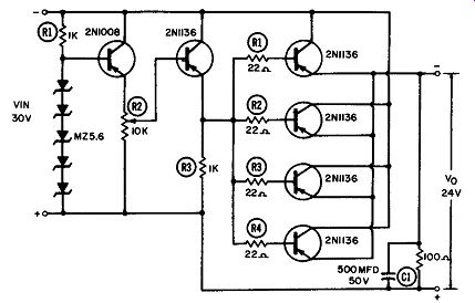
------------- Zener-controlled high-current regulator.
REGULATED POWER SUPPLY
This is a 115-volt AC regulated power supply in which the out put voltage remains constant for wide input variations. The value of secondary AC voltage should never exceed a maximum of 25 volts rms, and the output voltage should be less than one-half volt higher than the reference battery. If desired, the 6-volt battery may be replaced by a zener diode ( type A5B or equivalent). Half-wave rectifier D1 is made up of two paralleled 500-ma selenium rectifiers.
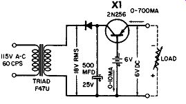
---------------- Regulated power supply.
150-WATT VOLTAGE REGULATOR
This is a 150-watt voltage regulator for use ( with a variable load) on a 117-volt line. The components used in this circuit are small, low-current devices, thus making it easy to mount the entire assembly in a small wall switch box for use in dimming a lamp load. Efficiency of this circuit is lower than the back-to-back arrangement of controlled rectifiers because of the added voltage drop in the diodes. This type of circuit is limited to systems operating at power frequencies and using standard silicon-controlled rectifiers ( SCR's) near their maximum ratings.
In this circuit a full-wave rectified voltage is applied to the SCR through diodes CR1, CR2, CR3, and CR4. On each half cycle the current will reach almost zero because of the three for ward-biased diode drops in series ( two diodes and the SCR). Thus, for a 117-volt, 60-cycle system, the current is reduced to microamperes for at least 20 microseconds during each half-cycle.
Because of the slow rise of forward voltage at the power frequency, this time interval is enough for the gate of the controlled rectifier to regain control of its anode. The SCR and its firing circuit ( using phase control on each half of the AC cycle) will then apply controlled AC voltage to the series load in the AC line.
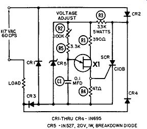
------------- 150-watt voltage regulator.

------------------(A) Waveshapes in switch.
----------------- (B) Electrical phase control. (C) Voltage-current waveform.
Phase-controlled AC switch.
PHASE-CONTROLLED AC SWITCH
Silicon-controlled rectifiers ( SCR' s) can be easily controlled by applying AC to their gate electrode, just as a thyratron can be controlled by applying the proper AC to its grid.
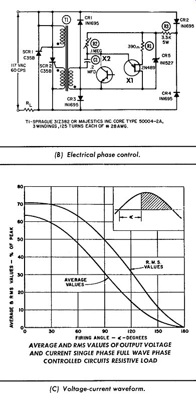
In this diagram, the SCR's are connected back-to-back ( or cathode-to-anode) across the input. Four diodes ( CR1 to CR4) form a bridge across the supply, with the control circuit ( X1, X2, and CR5) across the center of the bridge.
Part A-1 of the diagram shows the AC input, and Part A-2 shows the waveform developed across ( 1 ) the bridge rectifiers, ( 2) the zener diode, and ( 3) bridge load R3. The positive voltage ( Part A-3) that appears across UJT X1 also charges C1 through voltage control R2.
When C1 charges, it causes XI to conduct, thus discharging C1 through X1. This current flowing through T1 fires either SCR1 or SCR2 ( whichever anode is driven positive). The resultant waveforms are shown in Parts A-3 and A-5. When one SCR fires, the voltage across both of them decreases to approximately one volt. This keeps capacitor C1 discharged until the supply voltage is reversed. At this time, a new timing cycle starts for the firing of the alternate SCR. The firing angle of both SCR' s is controlled by potentiometer R2. Minimum output voltage occurs with R2 in its maximum position.
If desired, an NPN transistor ( X2) can be used to electrically control the firing angle. The circuit in Part B of the diagram shows how the voltage and current applied to a load can be con trolled. This is done by delaying the point in the AC cycle at which an SCR switches from the blocking to the conducting state.
Part C of the diagram illustrates the effect of this delayed firing on the average and rms output voltage and current in single phase, full-wave AC or DC resistive load circuits. This circuit can be used for lamp dimming, temperature control, and voltage regulation. By using the primary of a transformer for the indicated load, it is possible to control very high voltage or current loads on the secondary.
--------------
(A) 1N1763 half-wave rectifier.
(B)1N1764 half-wave rectifier.
(C) 1N1763 half-wave voltage doubler.
(D) IN1764 half-wave voltage doubler.
(E) IN1763 full-wave voltage doubler.
(F) 1N1764 full-wave voltage doubler.
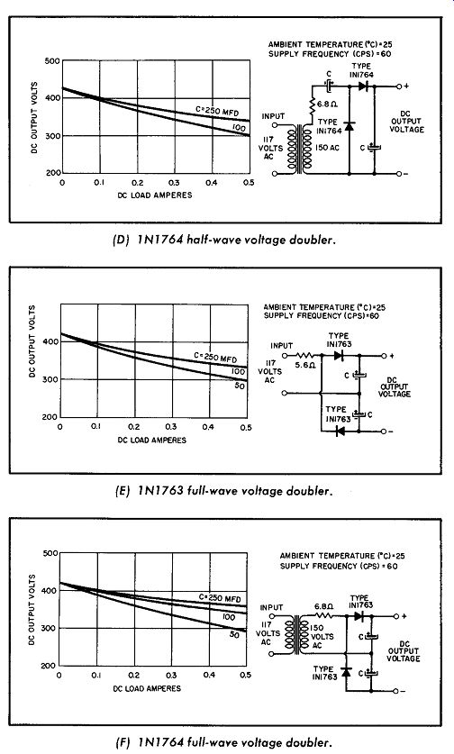
------------- Receiver power supplies.
RECEIVER POWER SUPPLIES
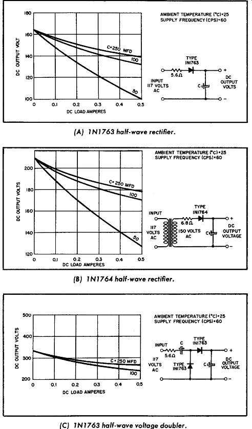
Some TV power supplies use either the IN1763 or IN1764 diode in their circuits, as shown in the diagram.
The INI63 has a peak inverse rating of 400 volts, and a rated DC forward current of 500 milliamperes. It also has a maximum reverse-current rating of 100 microamperes ( at the rated peak inverse voltage and 25°C. ambient temperature). This diode is intended for applications in which peak inverse AC voltages up to 140 volts are found. The INI 764, however, has a maximum peak inverse voltage of 500 volts; it is intended for rectifier applications subject to inverse peak voltages up to 175 volts.
Parts A and B of the diagram show the output and voltage current curves for half-wave rectifiers, while C and D show the curves for half-wave voltage doublers. Finally, E and F show full wave voltage-doubler circuits and their characteristic curves.
METER-CALIBRATION SUPPLY
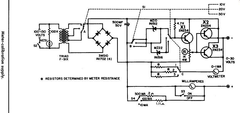
This diagram shows an adjustable regulated power supply for use in transistor testing or meter calibration. Voltages range from 0 to 30 volts, with a regulation of 0.1 % for an input of 100 to 130 volts. The supply has a multiratio power transformer for providing an adjustable voltage to the bridge-rectifier system.
On the 10-volt range, a 1N1512 zener diode is connected be tween the base of X1 and the positive bus, thus causing a regulated voltage to appear across potentiometer R1. A portion of this voltage is fed to the bases of parallel-connected X2 and X3 as bias. Since R1 sets the bias on these current amplifiers, it therefore controls the output voltage of the power supply.
On the 20-volt range, a 1Nl516 replaces the 1Nl512 and the maximum output voltage increases to 22 volts. On the 30-volt range the two diodes are series-connected, which allows a maximum output voltage of approximately 32 volts. On each voltage range the appropriate tap of the T1 secondary winding is selected to minimize the voltage drop across X2 and X3. This decreased voltage drop reduces both the collector dissipation and the collector-to-emitter voltage of X2 and X3. Thus, the bias across the transistors remains constant for the different input voltages. A fourth section of the range switch changes the multiplier resistor for the voltmeter.
Switch S4 changes the multipliers for the MA meter; and as a precaution against overload, S3 shorts the terminals when the meter is not in use. The resistances for the current or voltage meter depend on the particular meter used.
300-VOLT, 200-ma DC SUPPLY
This power supply provides 300 volts DC up to 200 mils. It is a high-voltage supply that can be used where size and regulation are important factors. Each leg of the bridge rectifier contains either one 1N540 or two 1N538's. Following the rectifier is a pi filter and the transistor regulator section.
The regulation of this supply is + 1 % from 0 to 200 ma DC, with an output ripple of less than 3 millivolts peak-to-peak.
SHUNT ZENER DIODE-TRANSISTOR VOLTAGE REGULATOR
Zener diodes used with transistors make effective shunt voltage regulators. The voltage-regulating factor of such a setup is improved by the current gain of the transistor used; hence, more power can be handled by the regulator.
----------------

--------------
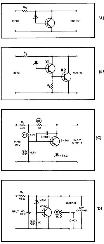
-------------- Shunt zener diode-transistor voltage regulator.
(A) Diode controlling 10-watt load.
(B) Diode controlling base of X1.
(C) Circuit for Vo higher than zener voltage.
(D) Circuit for Vo lower than zener voltage.
In Part A of the diagram, a I-watt zener diode can control a load of 10 watts, whereas in Part B the diode controls only the base potential of XL Here, X1 is used as an emitter follower and current amplifier with its collector-to-base voltage determining the bias on shunt regulator X2. If this regulator were to be used where an extremely large current variation is encountered, several shunt-connected transistors would then have to be employed in place of X2.
Part C of the diagram shows a shunt-regulated supply for out puts greater than the zener voltage (Vz). Here, the output voltage is determined by the formula R1+R2 Vo= R2 (Vz). For example, if R1 and R2 are the same value, the output voltage (Vo) will be twice Vz. Resistor R3 more or less compensates for variations in the supply voltage to the regulator. However, by using a potentiometer in place of R3, the exact value of variations can be compensated for. Excessive resistance at R3 should be avoided because Vo will drop as the input voltage increases. The output-voltage ripple will be less than 10 mv when the regulator is supplied by a full-wave rectifier with a 20-mfd capacity.
When lower than the zener voltage is required, the circuit in Part D of the diagram may be used. Here, the transistor collector-to-emitter potential is regulated by the diode, and the setting of potentiometer R2 determines the regulated output voltage. This potentiometer should have as low a resistance as possible, to minimize voltage variations due to load changes.
POWER TRANSISTORS AS DIODE RECTIFIERS
Since transistors connected in series have only a small voltage loss, they can be used for high-voltage applications. Inverse voltage and power dissipation are the two principal ratings to be considered when setting up simple rectifier circuits. Because of these considerations, power transistors ( which have low forward conduction characteristics) are quite useful as rectifiers.
Inverse voltage is that value of peak AC applied across the rectifier( s) in the reverse direction. It may be as high as 2.8 times the average DC output.
In Part A of the diagram, an example of series-connected transistors operating as a 20-ampere half-wave rectifier is shown.
For 117-volt line operation, the peak inverse voltage (PIV) of the four transistors in series will be approximately 400 volts. One watt, 5,000-ohm resistors are used, as shown, to prevent the entire 400 volts from appearing across any one transistor.
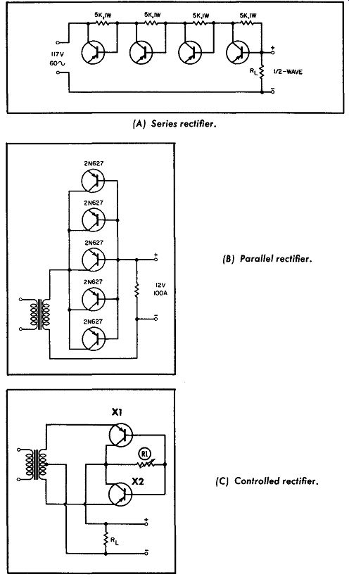
--------------209 Power transistors as diode rectifiers. (A) Series rectifier.
(B) Parallel rectifier. (C) Controlled rectifier.
Power transistors used as rectifiers have a small power loss due to their very low forward-voltage drop. A value for rectifier output-power dissipation is approximately 0.5 watt per ampere.
For a 2.5-ampere load current, these transistors do not require a heat sink at room temperature. However, for a load requiring 10 amperes, a heat sink capable of dissipating 5 watts must be provided; and at 20 amperes, the heat sink must be capable of dissipating 10 watts. In most equipment these heat-sink requirements are satisfied by anchoring the transistors to the chassis.
The transistors can be made to handle more power by operating them in parallel, as shown in Part B. Five 2N627 transistors may be used as a 12-volt, 100-ampere half-wave power supply. Center tapped or bridge-type power supplies can also be designed using parallel transistors.
A simple, controlled full-wave rectifier circuit is shown in Part C of the diagram. The current passed on each half-cycle ( limited by the load impedance) is controlled by the value of R1. As the resistance of R1 is increased, the base currents of X1 and X2 be come more and more limited, thus reducing the current applied to the load. The result is a very smooth and effective control of the output current and voltage.
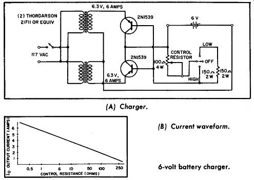
-------- 6-volt battery charger. (A) Charger. (B)Current waveform.
BATTERY CHARGER
A six-volt battery charger is shown in Part A of the diagram.
Two 6.3-volt transformers, each across the AC line, provide 12.6 volts. Two 2Nl539's are used as rectifiers, to control the DC current.
Three positions are available-low, high, and off. With the 150 ohm resistance in the circuit ( low position), current flow is as shown in Part B. Current flow on each half-cycle depends on this resistance, and is limited only by the load (battery) impedance.
ELECTRONIC RIPPLE Filter
An electronic power-transistor filter is very effective in reducing power-supply ripple. The filter capacitance across the load is approximately the value of the base filter multiplied by the current gain of the transistor.
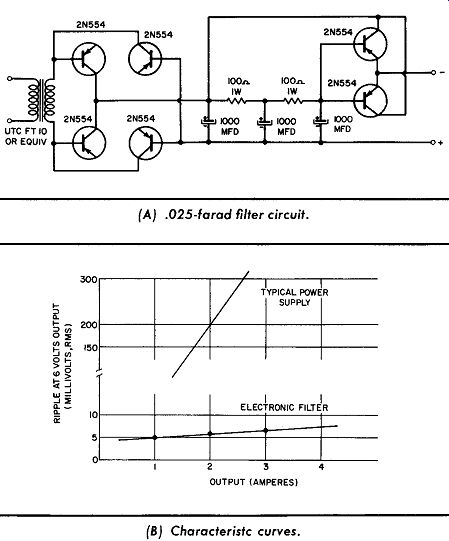
---------- Electronic ripple filter.
(A) .025-farad filter circuit.
(B) Characteristic curves.
-------------------
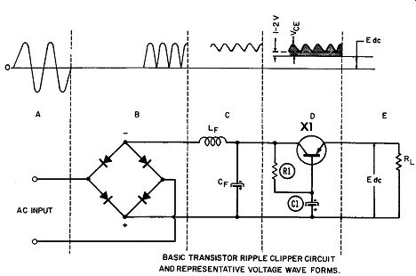
BASIC TRANSISTOR RIPPLE CLIPPER CIRCUIT ANO REPRESENTATIVE VOLTAGE WAVE FORMS. (A) Basic circuit with waveforms.
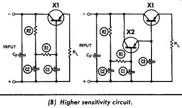
----------------- (B) Higher sensitivity circuit.
Ripple filters.
This capacitance multiplying factor results in an effective filter capacitance of 25,000 mfd in the circuit of Part A. The curves in Part B show the very low ripple voltages obtained at high load currents. Equally effective filtering by the conventional choke capacitance method would require the use of a very large and ex pensive inductor and/or capacitor.
This type of filter may be applied to almost any DC voltage power supply if a low collector-to-emitter voltage is maintained.
RIPPLE FILTERS
Acting as a variable series resistance, a power transistor makes an effective ripple filter for a DC power supply, where the gain of the transistor is a measure of circuit effectiveness.
Part A shows a basic circuit with (I) the AC input, ( 2) the rectifier output, ( 3) the output of the LC filter, ( 4) the voltage across the transistor, and ( 5) the circuit output. The shaded portion of ( 4) represents that part of the voltage dissipated in the transistor. The ripple filtering effect of the transistor is comparable to that in a conventional filter circuit, in which C2 is equal to C1 multiplied by the current gain of the transistor.
The ripple filter will be most efficient when the transistor is operated close to saturation. The minimum voltage drop across the transistor is I to 2 volts for the maximum load current expected. In Part B the use of decoupling network R2-C2 improves the circuit sensitivity, as does the addition of a second transistor.
Typical circuit values for Parts A and B are shown in Part C of the diagram.
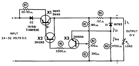
------------- Series voltage regulator.
SERIES VOLTAGE REGULATOR
Designed for an output of 21 volts with 1% regulation, this power supply provides an output current up to 3 amperes. voltage input can vary from 24 to 32 volts DC. This circuit operates by controlling the regulating impedance in series with the load. Here the variable impedance is a transistor which is controlled by comparing the voltage across R1 with a reference voltage, amplifying any difference in the compared values, and applying this difference to the regulating transistor. The end result is a closed loop in which the load cur rent is proportional to the difference between the measured load voltage and the reference voltage.
Diode D1 determines the reference voltage, and R4 limits the current through D1 to a nearly constant value. The combination of R1, R2, and R3 represents the output-voltage sensing network, a portion of which is compared by X3 with the voltage of D1.
The voltage difference between D1 and the portion of the output being compared determines the bias on X3. This difference is amplified by X3 and X2 and applied to X1, where it is again amplified and used as current control. R5 compensates for the difference voltage required to vary the current from no-load to full-load, and R6 limits the current through X3.
The tetrode power transistor ( X1) makes possible an improved series-voltage regulator for systems where current requirements vary widely. The second base connection provides good control of the total system leakage. This means the output terminals can be opened without loss of control and with very low standby cur rents. Good gain linearity assures constant regulation over wide current ranges. The degree of regulation can be selected and varied by means of current feedback.