AMAZON multi-meters discounts AMAZON oscilloscope discounts
BEFORE an automobile can be built, all the materials for its manufacture must be assembled. Since the same sort of thinking applies to the transistor, you now have one more clue to the purpose of the preceding section. We were getting the transistor's component parts all ready. These consist of n-type germanium and p-type germanium. And, just so that we can identify these
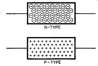
Fig. 201. We can represent n-type germanium (or any other semiconductor)
by a rectangle filled with minus signs. These indicate an excess of electrons.
For p-type germanium (or any other semiconductor) we can show a shortage
of electrons by plus signs.
items readily, we have drawings of n-type and p-type germanium in Fig. 201. These drawings, in their own exaggerated way, emphasize what we have already learned--that p-type germanium contains numerous atoms that suffer from electron shortages. Be cause of this, p-type germanium is shown as a rectangle with numerous plus signs scattered throughout. The atoms in the n-type germanium suffer from an embarrassment of richness--they have a surfeit of electrons and so we show this by numerous minus signs inside the little rectangle. More often, though, a semiconductor is shown in block form, as in Fig. 202.
Now you might very well object to the drawing in Fig. 201, since it may be difficult for you to regard the absence of an electron as a positive charge. But if you feel this way, consider a storage battery. One terminal is positive, while the other is negative. They are even stamped this way or have some other sort of identifying mark. But what is the true difference between the two terminals? The only real difference is that one terminal (the negative terminal) has far more electrons than the other terminal (the positive terminal). Note precisely what it is we are saying here. The terms negative and positive are relative. We do not say the positive terminal has no electrons; just that it has fewer electrons than the negative terminal.
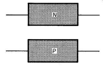
Fig. 202. A common method of representing n-type and p-type semiconductors
in block form. These are not electronic symbols.
Recombination and movement
Have you ever been in a train that was packed so tightly with people that no one could move? We hope you have, because the inconvenience you suffered will now help you one step forward in understanding transistors.
Imagine a train, with no seats at all. The train is absolutely jammed with people, packed so tightly that no one can possibly move. The train pulls into a station and just one person gets off.
This creates a vacancy (or hole) into which a person could move.
And so now we have a condition in which some movement inside the train is possible. Thus, one person adjacent to the vacant space could move into it; but in so doing, he would also create a vacant space into which the next person could move. The important thing to notice here is that movement is possible.
Now suppose that by this time the train pulls into the next station and one person gets on. This person occupies the only available space, and so movement stops entirely.
What sort of conclusion does this bring us to? Simply that if a person is to move, there must be a space for him (or her) to move into. This isn't a revolutionary idea, but what happens to our thinking if we apply it to an electron? An electron has ·mass and it occupies space. But here the analogy between people and electrons breaks down. An electron has a charge. When an atom loses an electron-or gains one-the net charge of the atom in creases or decreases (Fig. 203). The atom becomes more negative if it gains an electron, more positive if it loses one. And if an atom reverts to its status quo, it is neutral once again.
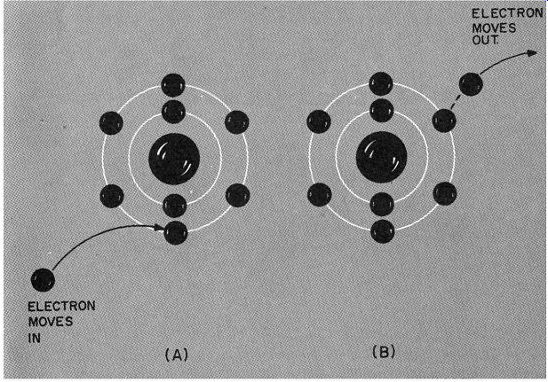
Fig. 203, An atom that has its regular quota of electrons is electrically
neutral.
It becomes an ion if it loses or gains an electron. If it gains an electron, it be comes a negative ion, as in drawing A. If it loses an electron (as in B), it becomes a positive ion.
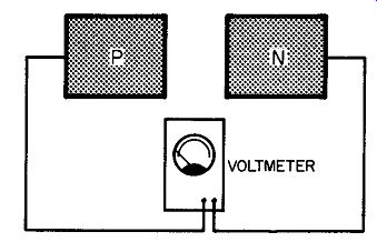
Fig. 204. The situation here is not the same as a battery. There is
no movement of electrons from n-type to p-type germanium.
Grand union
The ancient Chinese had a belief that the world was made of opposites, and these they called yin and yang. Many are immediately apparent--black and white, hot and cold, up and down, male and female, rich and poor. So it wouldn't surprise our friends of the far east if we came up with n-type and p-type germanium.
And because opposites have a habit of wanting to cling to each other, let's join our two types of germanium and examine the results. Before we do though, suppose we consider our two germanium types just a bit further.
Our n-type germanium is called that because it is electron rich. Unfortunately, though, this sort of language may create a wrong impression. Fig. 204 illustrates the problem. Here we have a block of n-type germanium and a block of p-type. We have a volt meter connected across the two, but the voltmeter reads zero. Why should this be so? Isn't the situation here exactly the same as a battery? Don't we have more electrons on one side than the other? To get the answer, think back to the way in which we made n-type germanium. We added donor atoms. In trying to adapt its own structure to the lattice structure of the germanium, the donor atom creates a condition in which an electron has been released so that it can travel. That is all that has been done. The net charge of the slab of the n-type germanium is zero. Similarly with the p-type. We have added an acceptor element with the result that the p-type germanium is in a position to allow the passage of electrons. That is all we have done and the net charge of the p-type germanium is also zero.
But now let's put our two blocks of germanium in as intimate contact as we can get them. In doing so we create a very pleasant situation for the germanium. The single-valence electrons of the donors in the n-type germanium will now move because there is good reason for them to do so. Not too far away from them is an area of p-type germanium with holes just waiting and receptive for any stray electrons. And so we get a recombination of electrons and holes.
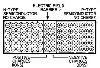
Fig. 205. The area at which n-type and p-type germanium (or any other
semiconductor) meet is known as a junction. In this area we get a diffusion
of electrons and holes. The result is a buildup of positive and negative
charges which stops any further diffusion. The charges form an electric
field, or barrier, which prevents any additional movement of charges.
Farewell to neutrality
The events that just took place did so at the junction of the two blocks of germanium (Fig. 205). Our first thought might be that all of the spare electrons in the n-type germanium and all the holes in the p-type would combine, but they are prevented from doing so. Let's consider the atoms at the junction. What has happened to the atoms of p-type germanium? The holes of these atoms (at the junction) have disappeared. They've been filled with electrons. But because of this these atoms are no longer neutral. The atoms have acquired an electron and so are negative.
Similarly the atoms of the n-type germanium (at the junction) have lost electrons and so are positive. These charged atoms at the junction form a barrier. This barrier is an electric field-or voltage, since we have had an electron movement.
Now we can see why all of the atoms in the p- and n-germanium do not swap charges. They can't. The barrier, or electric field, prevents the rest of the holes in the p-type germanium and the remainder of the electrons in the n-type germanium from getting together.
The electric field
We cannot dismiss the condition ex1stmg at the junction of n- and p-type germanium blocks so summarily. The reason we may not is that transistors work the way they do because of the barrier that exists. The barrier is the heart of the transistor.
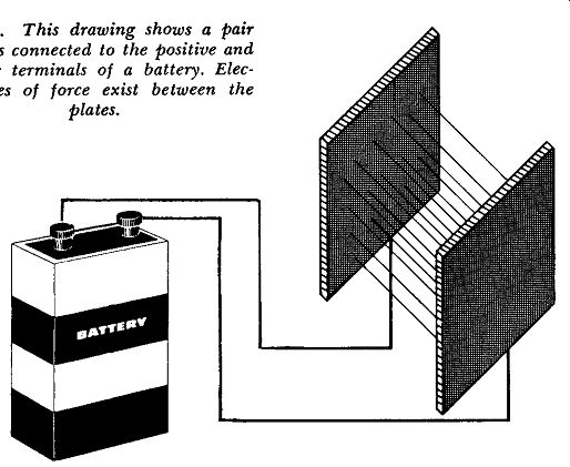
Fig. 206. This drawing shows a pair of plates connected to the positive
and negative terminals of a battery. Electric lines of force exist between
the plates.
Suppose, as shown in Fig. 206, we have a pair of metal plates connected to a battery. A force exists between the two plates.
We cannot see this force any more than we can magnetic lines of force, but it exists just the same. And just as we can draw imaginary lines to represent a magnetic field, so too can we draw lines between the two plates. We can call these lines an electric field.
If we were able to pick up an electron and deposit it in this electric field, the electron (carrying a negative charge) would promptly accelerate over to the positive plate. And if you could, without overstraining your imagination, pick up a positive charge and put it in the region of this electric field, it would just as promptly move to the negative plate.
But let's be contrary for a while. Suppose we did put an electron into the electric field and decided that we wanted it to go to the negative plate. The electron would oppose our efforts. For the electron the negatively charged plate is a force in opposition
- a sort of barrier. And we would have exactly the same results if we tried to push a positive charge toward the positive plate.
Again we would get that same frustrated feeling of opposition--a barrier.
Ionization
It is very easy to see, in Fig. 206, how we get our electric field. It is supplied by the battery. A battery is something tangible. We can buy it, we can touch it, we can connect it. But how do we get an electric field at the interfaces (the junction) of our two blocks of germanium? To get the answer to this question we must think about our atoms once again. Suppose we deprive an atom of an electron.
An electron, remember, carries a negative charge. So our atom, having lost a negative charge, is now considered positive--and quite rightly so. All we are really saying is that the atom isn't quite so negative as it was before the robbery took place. If our atom manages to acquire an extra electron we think of it as being negative.
Back in Section 1 we told you that atoms that gain or lose electrons are no longer the same. They have changed, and because they are different than they were originally, we call them ions. An ion is an atom that has gained or lost an electron. An ion is a charged atom and can be either positive or negative. An atom is neutral, but when it becomes an ion, that fence-straddling neutrality is gone.
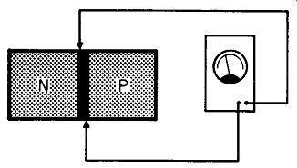
Fig. 207
Back to the barrier
Armed with this information, let us see how an electric field is set up at the junction. Electrons migrate from the n-type germanium. They are attracted to those beautiful open spaces which are really positive charges. But the departure of an electron from an atom changes it from an atom to an ion. All along the inter face of the n-type germanium we have ions. But what sort of ions? Since these atoms have lost electrons they must be positive, or plus, ions. What a strange thing to have happened. Out n-type germanium now has one side or face filled with positive charges.
What about the p-type germanium? The atoms along its face are gaining electrons. But if they are, they are no longer really atoms. They are ions--and negative ions at that! And so, facing each other (Fig. 205) we have positive and negative ions--or, more simply, positive and negative charges.
But how different is this from the charged plates in Fig. 206? If, in Fig. 206, we put a voltmeter across the charged plates, we would read a voltage. But isn't the situation the same in Fig. 207? In the case of Fig. 207, though, we did not need to depend on a battery to supply an electric field. Because of the ionization that takes place at the junction of the n- and p-type germanium, we have a measurable voltage. The effect is just as though we had somehow managed to insert a tiny cell between the two germanium blocks.
Going back to Fig. 205, we have a drawing which sums up what we have done thus far. We have two blocks of germanium--p and n--closely joined. Where they join, we have the formation of ions. On the p-side, the ions are negative. On the n-side, the ions are positive.
What about the electrons in the n-type germanium? How do they feel about all this? They would like to get across to the p-type germanium, but they are unable to get past the positive ions.
We have the same sad situation in the p-type germanium. Here the atoms would like nothing better than to play host to some electrons, but the negatively charged ions on their side stand in the way.
We now have an impasse. We have a potential, or voltage, across the interfaces of the two types of germanium. This is our barrier potential. The electrons in then-type germanium need some help at this point since, on their own, they just do not have enough energy to overcome the potential barrier. At this stage of the game, we have a p-n junction. This junction has its own electric field which keeps electrons on the n-side and holes on the p-side from getting together.
A matter of potential
We now have a rather odd situation. Here are two blocks of germanium--one n- and the other p-type. Each is electrically neutral. Yet some of the extra electrons in the n-type have moved across into the p-type. At the interface, the n-type, having lost electrons is now positive. And the p-type, having gained electrons, is now negative. This difference of potential, though, just exists at the interface.
Away with the status quo
We have been talking quite a bit about the potential barrier because it is so important to our story, but compared to the total number of available electrons in the n-type germanium, the amount that actually move are trifling. If we want to transfer any substantial amount of electrons, we're going to need to supply the electrons with energy. We could do it with heat, but there is a more practical method available.

Fig. 208. We can use a battery to force current through the semiconductor.
Fig. 208 shows the technique we are going to use. Here we have connected a battery so that the positive terminal is attached to the p-type germanium and the negative terminal to the n-type germanium. Electrons will now move from the negative terminal of the battery into the n-type. What is this motion? It isn't a calm or leisurely affair. The battery must overcome opposition, actually force or inject electrons into the n-type germanium. It's like get ting a shot for the flu. However cooperative the patient, and how ever sharp the needle, some amount of force is needed to accomplish the injection. In the case of germanium, the battery supplies the force, and the higher the voltage, the more force we have available.
What have we accomplished? We've injected electrons into the n-type germanium. But isn't this the germanium that, just a short time ago, lost some electrons at its interface? We even said that this region had become positive because of this loss. Now, we have re-supplied electrons to make up for that loss, so the number of positive ions at the n-side of the interface decreases. If we re duce the number of ions, though, what happens to our potential barrier? Since the potential barrier exists because of ionization, a reduction in the number of ions lowers the potential barrier.
Wasn't it the potential barrier that kept more than a limited number of electrons from moving across the interface? With the lowering of the barrier, electrons can now move across from the n- to the p-type germanium.
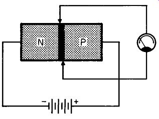
Fig. 209. The application of a voltage to the n- and p-type semiconductor
reduces the potential barrier.
What's going on here?
When we first joined n- and p-type germanium, ionization, caused by movement of holes and electrons, could not exist until the two blocks of germanium were physically joined. When we finally did unite the germanium we obtained ionization on both sides. The voltage across the barrier--the barrier potential--soon put a stop to further movement of any charges. But if we lower the barrier potential, we lower the hindrance.
Does this mean that we eliminate the barrier completely? Not at all. We have lowered the potential difference across the inter face but we haven't done away with it completely, since we will have ions constantly being formed. The situation has changed because we are now able, with the help of the battery, to de-ionize many of the ions being formed. Most--not all--of the atoms that lose electrons (hence become positive ions) will receive electrons because of that electron storehouse--the battery (Fig. 209). Up to now, though, we have been neglecting the positive terminal of the battery and the bit of p-type germanium to which we have connected it. The positive terminal of the battery is characterized by a very important feature. It does have electrons--but far, far fewer than the negative terminal of the battery. What effect will this have on the p-type germanium? Actually, we should have been speaking about the ions at the interface. What sort of ions are these at the p-type interface? In this case we are dealing with negative ions--atoms that have one electron more than in their neutral state.
These negative ions now have a wonderful chance to become neutral once again. Their extra electrons, heeding the siren call of the positive terminal of the battery, soon start to move in that direction. Again we have de-ionization, only this time it is the negative ions that become neutral.
Let's recapitulate what happens when we connect our battery.
The positive ions at the n-type interface acquire electrons and so de-ionize. The negative ions at the p-type interface lose electrons and so de-ionize. With de-ionization taking place on both sides, the potential barrier is lowered.
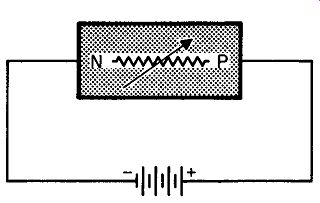
Fig. 210. The potential barrier acts like a variable resistor. Its value
at any moment depends on the battery and the diffusion taking place at
the interfaces of the n- and p-type semiconductors.
What happens to the electrons from an overall point of view? They move from the negative terminal of the battery, through the n-type germanium, across the lowered barrier, through the p-type germanium over to the positive terminal of the battery.
How many electrons will flow? That depends on the potential barrier. If it is low, more current will flow. If it is high, less cur rent. We can, if you like, regard the barrier as a resistance (Fig. 210). With a comparatively large potential barrier, we'll get small current flow. A large potential barrier would correspond to a high value of resistance.
Hole movement and electron movement
How shall we regard the movement of charges in our diode? We have three choices. We can consider it from-the viewpoint of electron flow. Or we can think of it as hole flow. Actually, it is both, but there is a practical aspect we must consider. As long as we confine our attention to the germanium, and to the germanium only, the true action is a movement of electrons and holes, and in opposite directions. But the transistor is simply a means to an end. It will be used, just as a vacuum tube is used, to control current (electron) flow. Thus, in all circuits external to the transistor, in the wiring and the various components we are going to connect to the transistor, we are only going to consider electron flow, for that is all that will take place. Recombination--the re-union of holes and electrons, hole and electron movement combined, takes place only in the transistor. Outside the transistor we have only electron movement.
Why, why, why?
It might seem that what we have accomplished thus far is not too important, but consider what has been done. We took germanium, which in its pure state is an insulator, and made a conductor out of it. But to do this required that we trick the germanium in some way. We did this by making one block of it so that it had an electron surplus, and another block so that it had an electron deficiency. When we joined the two blocks we did get a small amount of current drift, and if electron movement had not been blocked by ionization, we would have had a gradual diffusion, a gradual equalization of electrons on both sides. That equalization is never reached, since, when we connected a battery to the germanium, electrons were coaxed into entering the positive terminal of the battery as fast as electrons departed from the negative terminal.
Forward bias
We have so many different sizes, shapes, styles and chemical arrangements in batteries, that the word battery, used by itself, is somewhat meaningless. If we say flashlight battery, auto battery or filament battery, then the modifying word adds some sense; it paints a picture. The battery that we used in Fig. 209 also needs a name. It is a bias battery. And because this battery helps over come the potential barrier, because it makes numerous electrons march where relatively few moved, we call it forward bias. Note well that in forward bias the negative terminal of the battery connects to the n-block of the semiconductor; the positive terminal to the p-block.
Reverse bias
The opposition to the flow of current, that is, to hole movement and electron movement, that exists as a result of the potential barrier can be lowered by using forward bias. But the control of current flow is not really complete if all we can do is to increase it.
To see how we can raise the opposition to current flow, look at Fig. 211. We are still using our two blocks of p- and n-type germanium. They are still in very intimate contact. The only change we seem to have made is to transpose the battery. But this reversal of polarity produces important changes at the junction of the two germanium blocks.
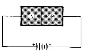
Fig. 211. Reverse biasing of a semiconductor diode.
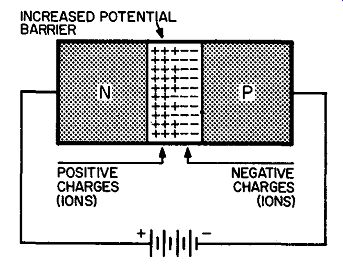
Fig. 212. Reverse biasing increases the potential barrier.
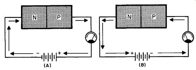
Fig. 213. The drawing in A shows forward biasing; the one in B is reverse
biasing. Although current flows through the diodes in opposite directions
its movement is still from minus to plus.
The drawing in Fig. 212 shows that the number of ions on both sides of the junction has increased. We have more negative ions and we have an equal amount of positive ions. But the formation of ions on both sides results in a potential difference. This potential difference, or voltage, is our barrier, hut now our barrier is stronger than it ever was.
What has produced this condition? The positive terminal of the battery, connected to the n-type germanium, has provided a haven for electrons. Some of these move into the positive terminal of the battery. At the same time an equal amount of electrons move way from the negative terminal of the battery into the p-type germanium.
In Fig. 213 we have a drawing in which we can compare the two ways in which we connected a battery to the semiconductor.
In both cases the electron current flows away from the negative terminal of the battery, toward its positive terminal. And yet, as you can see by the arrows, the currents flow in opposite directions through the transistor. To emphasize the opposite flow of current, a semiconductor diode that has a reverse (or opposite) flow of current is said to be reverse biased.
A matter of degree We can get forward current or reverse current, depending entirely on how we connect our battery to the semiconductor diode.
But there is an implication of equality here that is not true. Re verse current is small, generally measured in terms of microamperes. Forward current is large and is usually milliamperes or amperes. But you can no more consider current by itself than you can operate a seesaw alone. High current connotes low resistance.
Similarly, low current means that its opposite, resistance, is way up in the air. Forward biasing is just another way of saying low potential barrier or low resistance at the junction. Reverse biasing goes hand in hand with high resistance at the junction or a high potential barrier.
The diode
It may seem to you a little late in this section for us to give a name to our two blocks of germanium. It is known as a diode, a rather lazy selection, since the name was borrowed directly from its vacuum-tube counterpart. The dictionary definition is certainly not applicable. The prefix is di (from the Greek dis, meaning two) while the suffix is ode (from the Greek hodos, meaning a way or path). Thus, a diode has two paths, and if we think of the forward and reverse flows of current, then perhaps the name diode isn't too poor a selection after all.
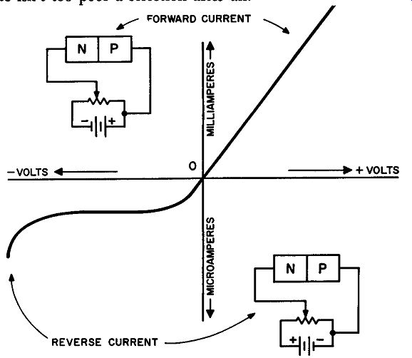
Fig. 214. Forward and reverse currents of a semiconductor diode.
Graphs
Now you might wonder why we have spent so much time on the diode, since our basic interest is the transistor. There are a number of good reasons for this. The transistor (as we shall learn in our next section) is developed directly from the diode. To under stand how the transistor works you must first know what happens in the diode. Actually (again, as we shall learn later) the transistor can be considered as a pair of diodes, back to back, so you are really studying transistors, possibly without realizing it. Finally, transistors can be used as diodes.
In Fig. 214 we have the graph of the forward and reverse cur rents of a semiconductor diode. Let's examine the graph to see what information we can extract from it. First, consider the situation in which the diode is forward biased. As the voltage is gradually increased the forward current increases. Now consider the case when the battery is transposed. As the voltage is increased, we get a very small rise in reverse current. Note, in the instance of reverse bias, that the reverse current remains fairly uniform for a large part of the curve.
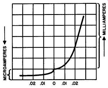
Fig. 215. Forward and reverse currents of a semiconductor diode. As
the for ward bias is increased, the current in creases gradually ( at
first) but a point is soon reached where the current takes a sharp rise.
The reverse current is much smaller than the forward current, is measured
in microamperes. In this diode the forward current is in milliamperes.
The difference is much more marked than would seem offhand since it takes
a thousand microamperes to make up one milliampere.
Fig. 216. If the reverse bias is in creased, a value is reached at which the reverse current increases drastically. This is at point X in the graph.
It is also very important for you to see that the forward current is plotted in milliamperes and the reverse current in microamperes. Technically, both curves should have been plotted in the same units but even here you can see that relatively, the forward current is far more substantial than the reverse current.
While the graph of Fig. 214 is useful as a comparison between forward and reverse currents, it does not supply an adequate picture in the region near zero voltage. It is close to this point that the potential barrier exists and, graphically, we are interested in seeing what happens to it. Fig. 215 is an enlargement of the graph close to the zero point. As we increase our forward voltage, from zero to .01, there is a bare increase in current. This tells us that we have not yet overcome the potential barrier. But look what happens to the curve as we reach .01 volt. The current rises dramatically. Since this occurs at approximately the .01-volt point, we can assume that this was the value of the potential barrier.
Now let's examine the reverse current in the same way--near the zero-volt point. Here there is a small, but steady, increase in reverse current, as we go from zero to .01 volt. But beyond this point the current levels off.
How high is high?
With the p-n diode, as with everything else, a limit exists some where. Fig. 216 illustrates this very nicely. As we increase the reverse bias, the reverse current remains quite uniform. But when we hit a certain voltage point we get an extremely abrupt increase in current. Increasing the voltage beyond this point has no effect, since the maximum reverse current 1s now going through the diode.
To understand what has happened we must go back to our potential barrier. With the application of reverse bias, the potential barrier increases. But this barrier is a voltage, and so there is an electrostatic stress between the two ionized regions--one in the p-type germanium and the other in the n-type. This stress--or field--is a strong force. Electrons that would normally be quite content to remain in the outer orbit of their atoms, are pulled away. Of course, in moving out of position, they leave holes thus creating quite an opportunity for other electrons to get moving.
Still more electrons are added to the general stampede through collision--electrons being knocked out of orbit, just as a pedestrian could get bowled over by a mad rush of people.
What we get now is a flood, an avalanche of electrons--and the graph in Fig. 216 shows this very well. The whole chain of events we have described is called avalanche multiplication. The critical point at which this multiplication of electrons in motion starts, producing a current that is independent of voltage, is called avalanche breakdown. Point X on the graph is the avalanche break down point.
The Zener diode
Earlier, in Fig. 212, we showed you a magnified view of the interface region in the n-p diode. Where the battery voltage is below the critical point we get a small current. Above the critical point, the current through the interface is large, the voltage across the interface is constant.
Now you might think (and quite correctly, as far as transistors are concerned) that we don't want this avalanche effect. For certain applications, though, this sudden transition from small to large current is very useful. Some diodes are manufactured especially to take advantage of this characteristic. They are known as Zener diodes.
Our interest in the Zener diode stems from the fact that we are going to use them in conjunction with transistors. Also, any transistor with sufficient reverse voltage will suffer the avalanche effect.
Resistance characteristic We've been talking about voltage and current, but whenever we do, you can be sure that you will find resistance lurking some where about. Fig. 217 is the graph of the resistance characteristic of a semiconductor diode. But while we refer to it as a resistance characteristic, it is really a measure of the effectiveness of the potential barrier. Examine the curve in the region of zero volts.
Put your finger at the zero mark and then move up on the vertical line until you reach the curve. The value here is somewhere be tween kilohms and megohms. From here we can move down on the curve in the direction of forward bias. As the forward bias overcomes the potential barrier, we get a decreased opposition to current flow. This is just as though we had reduced the resistance at the junction.
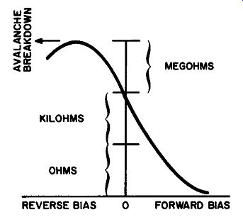
Fig. 217. Diode characteristics can be interpreted fn terms of resistance.
An increase in forward bias results in a de crease in resistance. An
increase in reverse bias raises the resistance.
Moving in the other direction, you can see that the resistance curve rises to a peak. This peak is really a plateau, for the resistance remains high, remains uniform. But as we move further to the left we are moving in the direction of higher reverse bias. At some voltage we will reach the breakdown point, and, of course, the resistance will take a precipitous drop.
A few implications
A graph is more than just a pretty picture and there is a lot more significance to the curve in Fig. 217 than its resemblance to a scenic railway. What we are really saying is that we can control resistance by means of voltage. Now this might not seem like a startling innovation until we remember that we ordinarily think of current as being controlled by voltage. Ohm's law emphasizes this for us in no uncertain terms. But in Fig. 217 we have managed to adjust the resistance of our diode in two ways. The first depends on polarity--that is, whether we are forward- or reverse-biasing our diode. And the second is predicated on the amount of bias voltage used.
In the meantime, you may have noted that, while we discussed the effects of an excessive reverse voltage, no mention has been made of excessive forward voltage. This bit of information is being reserved for the discussion on transistors.
The transistor cometh
Since the start of this guide there has been implied a promise to talk about transistors, and it would seem as though that promise has not been kept. And yet, as you will see in your next section, we are going to need every bit of information we have gathered so far to understand and use transistors.
QUIZ
1. What is reverse bias? Forward bias?
2. What is a negative ion? A positive ion?
3. Describe ionization at the p-n junction.
4. What is the potential barrier? How can we increase it? How can we decrease it?
5. What is electron injection?
6. What is avalanche voltage? Avalanche current? What conditions produce avalanche current?
7. What is the name of the battery connected to the p-n diode?
8. In terms of quantity, what is the difference between forward and reverse current?
9. What is the relationship between the resistance of a p-n junction and the potential barrier?
10. What type of field is set up between blocks of p- and n-type germanium in close contact?