AMAZON multi-meters discounts AMAZON oscilloscope discounts
THE transistors we have been discussing thus far have all been lumped into two very broad and general categories. They have been either p-n-p or n-p-n units, but other than the fact that we have designated them as triodes, we have said nothing to you so far to give you a hint that there might be some very strong differences in transistors. The electronic symbols for an audio power transistor and a converter transistor will look exactly alike, and yet the operating requirements for these transistors are opposites.
The output transistor must handle power at comparatively low frequencies. The mixer is much less concerned with power but works at considerably higher frequencies. Obviously, since their functions are so dissimilar, there must be considerable differences in the way they are fabricated and packaged.
Transit time Although we may be inclined to look on the electron as a speedy little cuss, yet electrons can be slowed when they encounter obstacles and barriers, just like people. Consider the electron in a vacuum tube. If we have a triode, nothing (with the exception of the control grid) stands in the way of a rapid passage from the cathode to the plate. And even here we make the grid as much of an open mesh as possible so as not to interfere with electron travel.
But what do we have in the transistor? Instead of open space, we have a crystal lattice structure, and so we are, in effect, forcing the electron to hop from one atom to the next. But the frequency at which we can operate is determined by how fast we can get the electron from the emitter to the collector or from the collector to the emitter. And, quite unlike the tube, we always have a barrier between these two electrodes. This barrier is the base, and while we can make the base extremely thin, the fact remains that the base exists between the collector and emitter. (A typical value of base thinness would be .001 inch or less.)

Fig. 701. The diode has some resemblance to a capacitor.
There are other factors which tend to limit the frequency range--that is, the upper limit of frequency at which the transistor will operate. One of these is the capacitance existing between the transistor electrodes. In Fig. 701-A we see how we can come to regard the transistor as a capacitor. Here we have the p-n section and, as you will observe, the diode is reverse biased. Current flows initially, but ceases shortly thereafter, because of the build-up of opposing charges at the junction between the two blocks of semiconductor material. But isn't this action very remm1scent of the way a capacitor charges. When we connect a capacitor to a battery as in Fig. 701-B, there is a momentary rush to charge the capacitor. The current flowing in the circuit rapidly drops as opposing charges collect on the plates. In the transistor, the effect is just as though we had a capacitor in shunt with the elements of the transistor. But as we go up in frequency, the reactance of this shunting capacitor becomes less and less, and, if the frequency is high enough, acts like a virtual short across the transistor.
There is still another factor with which we must contend when considering transit time and that is the material of which the base is made. We will get swifter movement of electrons through certain semiconductor materials than through others.
Alpha cutoff frequency
As we increase the frequency of a signal to be amplified by a transistor, there will come a point at which we will simply be wasting our time, for there will be no amplification. The transition from a condition of gain to one of no-gain isn't an abrupt change. As a basis for comparison among all transistors, we can establish the gain of a transistor at 1 khz as standard. We can consider the practical operating limit to exist when the gain drops to .707 of the gain at 1 khz (as we increase the frequency). This is known as the alpha cutoff frequency.

Fig. 702. The tetrode transistor gets the effect of a reduced base area
by applying an additional bias to it.
The tetrode transistor
We have now revealed the base as one of the chief culprits in limiting alpha cutoff frequency. This means that if we want to increase the operating frequency of a transistor we must force the base to yield to some sort of treatment. There are various pleasant ways of doing this, one of which results in a unit known as a tetrode transistor.
At this point you have probably jumped headlong to a wrong conclusion, based on your experience with vacuum tubes. In the tube we make a tetrode by adding a fourth element known as a screen grid. The name tetrode means four elements, so applying it to the transistor is somewhat misleading.
Fig. 703. Electronic symbols for p-n-p and n-p-n tetrode transistors.
In Fig. 702 we have a block diagram of a tetrode transistor. All we have really done, though, is to add another lead to the existing· base. Basically, what we have is a transistor, with the added lead biased negatively with respect to the base. The transistor can be either a p-n-p or an n-p-n type, but, as you can see, the one in Fig. 702 is an n-p-n. Since we now have two base leads, one is identified as base 1 and the other as base 2. The transistor is for ward and reverse biased in the usual way. R1 and R2 are the biasing resistors for the base-emitter input circuit. A single battery, B2, supplies both forward and reverse bias for the transistor.
However, we have an additional battery, B1, connected between base leads 1 and 2.
Now examine the lead going to base 2. It is connected to the negative terminal of B1, and so, apparently, we have made the base negative with respect to the emitter. But this isn't entirely correct, since the other base lead (#1) is connected tapped up on voltage divider R1-R2. But how do we want the base biased? Since we have an n-p-n unit, we want the base to be positive with respect to the emitter. The effect of B1, then, is to reduce the amount of area of the base that is really positive with respect to the emitter. But reducing the area gives us the same effect as reducing the volume of the base. Since the alpha cutoff frequency depends on the thickness of the base we have increased our avail able operating frequency. Actually, the situation is a little better than we expect, since the alpha cutoff frequency varies as the square of the thickness of the base. Thus, if we manage to cut the thickness in half, we raise the alpha cutoff frequency by a factor of four. If we cut the thickness. to one-third of the original, we in crease the alpha cutoff frequency by nine. As you can see, the re wards are great for this effort.
Just as we have symbols for n-p-n and p-n-p triodes, so too do we have symbols for n-p-n and p-n-p tetrode transistors. These are shown in Fig. 703.
Fig. 703. Electronic symbols for p-n-p and n-p-n tetrode transistors.
The surface-barrier transistor
Since our objective (at the moment) is to get a high-frequency transistor and since we can do this by making the base thin, why not shave the base down as much as possible? This may sound terribly difficult, since the thickness of the base is often fractions of a thousandth of an inch, but it can be done. When we do this, we solve one problem only to be faced with another. How do we fasten a lead to something that must be so thin? A pleasant and practical solution to this problem is achieved by the surface barrier transistor. We have a sliced-through section of one of these in Fig. 704.
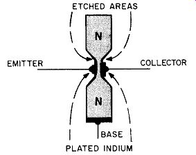
Fig. 704. The surface-barrier transistor uses a single section of n-type
germanium.
The effect is that of a p-n-p transistor. Most of the base remains just as it is in an ordinary transistor. However, in the region between the emitter and the collector, the base material has been etched away, and as a result the emitter and the collector may be separated by as little as ten thousandths of an inch. Since the remainder of the base is as thick as it was before, there is no additional problem of fastening the base lead.
We now have two techniques for reducing base thickness. One is electrically, as in the tetrode transistor, and the other is physically, as in the surface-barrier. In both cases we must pay a price to get what we want, and the price is a reduction in power handling capabilities. An electric strain exists between emitter and collector due to the battery. By reducing the thickness of the base, we have really brought the negative and positive terminals of the battery much closer (electrically) to each other.
The surface-barrier transistor, though, is not quite the same as all the other transistors we have studied. The base is a single crystal or wafer of n-type germanium, and that is all--no p-type germanium is used. The emitter and collector electrodes are made of a metal called indium. These metals are plated onto the etched out part of then-type germanium wafer. The metal does not melt or diffuse into the germanium, simply forming a plated electrode.
We do have a barrier, though, just as in any ordinary transistor.
This barrier exists between the plated electrodes (emitter and collector) and the base, and as a result we get the equivalent of transistor action.
The symbol for the surface-barrier transistor is the same as for a p-n-p unit, and is treated as such with respect to bias. That is, the emitter is made positive, the base less so, while the collector is negative with respect to the emitter.
The element, indium, selected for the emitter and collector of the surface-barrier transistor, belongs to the acceptor group, gallium, boron and aluminum, mentioned in an earlier section.
Since it has but three electrons in its outermost ring, indium is short an electron, hence the p-type designation. For this reason, all surface-barrier transistors using indium for emitter and collector, and n-type germanium for the base must be of the p-n-p type.
There is a very important difference between the surface-barrier transistor and all the others we have studied so far. In the usual transistor, the semiconductor material is doped with an impurity--either donor or acceptor type--to form n-type or p-type semiconductor material. In the surface barrier transistor, however, just one element is so treated--and that element is the base, made of n-type germanium. The other electrodes, the emitter and the collector, consist of a small plated area of a metal-indium.
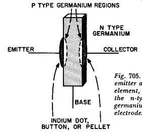
Fig. 705. The diffused transistor has an emitter and collector made
of an acceptor element, indium. The indium, melted into the n-type germanium,
creates p-type germanium in the immediate region of the electrodes. This
results in a p-n-p transistor.
The diffused transistor
There is still another type, the diffused transistor, which seems to resemble the surface-barrier transistor, yet possesses a very significant difference. The diffused transistor appears in Fig. 705.
In this transistor, as in the surface barrier transistor, we start with a section of n-type germanium. This is our base. A small amount of indium is melted into the base on each side, forming the emitter and collector. The melting process is continued until the emitter and collector almost touch each other, resulting in a very narrow base region between them. This is just what we want, of course, to permit a high alpha cutoff frequency.
When the indium melts into the germanium, we get the effect of doping the immediate region around the indium. And since indium, as we mentioned earlier, is an acceptor impurity, the result is that we get the formation of p-type germanium in the region of the impurity.
Note the difference between the surface barrier and diffused p-n-p transistors. In the surface-barrier transistor, the indium is just a plated electrode. There is no physical penetration into the n-type base. The surface-barrier transistor depends on an etching process to reduce the base thickness. The diffused transistor depends on the melting of the indium to narrow the base. For both types of transistors, the symbol is identical--and is that of a p-n-p transistor.
Micro-alloy transistor There are different methods used in putting the emitter and collector electrodes onto a surface-barrier type transistor. They can be plated on or they can be alloyed as a very thin film of metal on the n-type germanium base. This produces a unit known as a micro-alloy transistor. An alloy consists of two substances that are melted or diffused into each other and so, in this respect, the micro-alloy transistor is more closely related to the diffused transistor.
In working with transistors you will come across many rather descriptive names, perhaps g1vmg you the idea that these transistors must be radically different in many respects. As you can see from our description of the diffused transistor, the surface barrier, and the micro-alloy transistor, one of the biggest differences is in the way the particular transistor is manufactured. The micro-alloy transistor, as an example, is sometimes referred to as a MADT--a micro-alloy diffused-base transistor. And, to compound the growing confusion, this same transistor is often called just an alloy-diffused transistor, or an alloy transistor. The alloy material, indium, is termed a dot or button, because of its shape on the surface of the n-type germanium base.
Manufacturers of transistors often use names of their own to describe transistors, sometimes creating the impression that there must be many different types of transistors. Thus, what we have called a diffused transistor is also called a diffused junction transistor, a fused transistor, a fused junction transistor, a diffused emitter-collector transistor, a diffused E-C transistor, graded dif fused, or (quite strangely) drift transistors. The tetrode transistor, described earlier, is also known as a double-base junction transistor. These are not all, because there is no doubt that we must have missed a few, or somewhere there must be a manufacturer concocting still another name. If you come across a transistor whose name seems unusual (and you will) stop and reflect for a moment. It may be just the name that is new--not the transistor type.
Junction transistors
These are the workhorses in transistor radios and are the units we used in describing our audio, if and rf amplifiers. And, as we have emphasized so often, they come in two basic types--n-p-n and p-n-p. A receiver may use n-p-n's, p-n-p's, or both, in a single set. P-n-p's seem to be more popular for radio receivers.
Before you rejoice over the fact that the name for this very widely-used transistor type is so simple and easy to remember, it is our sad duty to inform you that like almost all other transistors it is available under a variety of names, the choice depending upon the semantic ability of the manufacturer's engineering department. Thus you may find the junction unit listed as a fusion alloy junction transistor or alloyed junction transistor. Either germanium or silicon can be used as the semimetal, and so this information is often included in the name. We will then get names such as silicon fusion alloy junction transistor or germanium fusion alloy junction transistor.
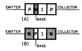
Fig. 706. An intrinsic transistor raises the alpha cutoff frequency
by reducing capacitance between collector and base.
Intrinsic transistors
These are also known as intrinsic-region transistors, p-n-i-p transistors, n-p-i-n transistors. Unlike the surface-barrier and diffused transistors in which we try to make the base as thin as possible, the intrinsic transistor may actually increase the base thickness and yet have an extremely high alpha cutoff frequency.
This may seem to contradict what we said earlier so let us ex amine Fig. 706 to see if we can come to some sort of reconciliation.
As you can see, in Fig. 706-A, we have what appears to be an ordinary p-n-p transistor, but sandwiched in between the base and the collector, we have a block of material marked with the letter I. This letter I is the first letter of the word, intrinsic. The intrinsic region consists of a semiconductor that is free of any doping impurity. This means that the semiconductor has an equal number of holes and electrons, hence is neither n-type or p-type. Since its facilities for current flow are very poor, it has a high resistance.
The virtue of the intrinsic region is that it separates the collector and the base. This is like moving the plates of a capacitor further apart. When we do this, we reduce the capacitance. Earlier we mentioned that one of the hurdles a transistor must overcome is capacitance between electrodes. In an ordinary junction transistor, the base (input) and the collector (output) are in intimate contact. This makes the capacitance large enough to lower the alpha cutoff frequency considerably.
There is probably one statement that is now worrying you and that is the high resistance of the intrinsic region. If it is, think of the resistance that appears between cathode and plate of the ordinary vacuum tube. In power tubes or power transistors, where we work with high values of current, resistance between elements is important and we want it to be as low as possible. But for rf work, where the current in a transistor (or in a tube, for that matter)
is so very small, high resistance does not seem to be detrimental.
The intrinsic transistor comes in two types, as shown in Fig. 706-A and 706-B.
Fig. 707. Hook transistor resembles combined p-n-p and n-p-11 transistors.
Hook transistors
Every cook has a specialty, and those that feature soup, come up with some surprising (and often tasty) combinations. The true culinary artist will put anything and everything into the soup (at least once) just to see what will happen. So too in electronics do we have engineers who will try anything once. The more successful of these artists graduate to transistor design, where we can recognize their deft hands in the manufacture of unusual transistor combinations. One such is known as the hook transistor, or four-layer triode.
We have an example of this transistor in Fig 707. At first glance it looks as though we have a pair of p-n diodes, but we can wipe our glasses and look again. Now you can see that what we really have (reading from left to right) is a p-n-p transistor or (starting at the base) an n-p-n transistor. If this shocks you, consider a cascade circuit in which we go from the cathode to the plate of one tube, and then immediately into the cathode of the next.
Getting back to the hook transistor, the chief difference is in the way the collector is constructed. It has a slice of p-type germanium sandwiched in between itself and the base. With this sort of an arrangement, the hook transistor is most unusual in that it has an alpha greater than 1. No other transistor has such a characteristic except the point contact, the original transistor to be developed and which is now obsolete. Unlike the usual grounded emitter transistor arrangement, the hook transistor has an output which is in phase with its input.
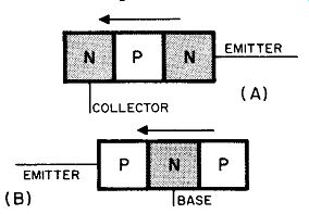
Fig. 708. The hook transistor can be separated into an n-p-n, as in
A, and a p-n-p, as in B.
Now let's consider the n-p-n side of this unusual combination.
Starting at the extreme right we have n-type germanium and we have marked this as collector for the entire hook transistor, but right now let's think of it as the emitter for the n-p-n. From here we pass to a base which has no connection, and then to the n-germanium marked base but which is really the collector for our n-p-n transistor. Since this is all very confusing, suppose we separate the n-p-n section as in Fig. 708. In a typical n-p-n transistor we would have a negative voltage at the emitter and a positive voltage at the collector. But this is exactly what we have, since the collector in Fig. 708 is the base of the hook transistor and so really has a positive voltage on it. We haven't put any voltage on the p-section. This acts as the base of our n-p-n unit, but it isn't biased in the usual manner. Because of the thinness of the base, electrons have no problem in flowing from the emitter to the collector. Note the direction of current movement for the n-p-n transistor. As you know, in an n-p-n transistor, current moves from emitter toward collector, and so the drawing in Fig. 708-A fulfills this requirement.
Right below Fig. 708-A, in Fig. 708-B, we have the remainder of the hook transistor. This is the p-n-p section and, as usual in this type of transistor, current flows toward the emitter. Now if we recombine our two transistors into the single unit of Fig. 707, we have two currents, and the output coming out of the emitter is the sum of the two.
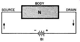
Fig. 709. We start our field-effect transistor with a core of n-type
germanium, connected to a battery.
Field-effect transistor
Before we begin with the next transistor, let's list its other name. It is also known as a unipolar transistor. We can start our construction of the unit with a single block of n-type germanium, as in Fig. 709. We can regard the germanium in this case just as we would a resistor. We will call the germanium the "body", the connection at the left side the "source" and the exit point for the electrons, the "drain". The electrons flow through the entire body, utilizing the full volume of the body for passage from the left of the unit to the right.
Our next step is to put a jacket of p-type material around the body, as shown in Fig. 710-A. It may be a little difficult to visualize this from a cross-sectional view, but Fig. 710-B will give you a better idea of the construction. The jacket of p-type material is entitled to a name of its own, and so we will call it a gate. We have added another battery (B2) in the drawings in Fig. 710 and have arranged the battery so the gate is biased negatively with respect to the body.
We now have a negatively charged semiconductor surrounding another semiconductor through which electrons are bravely moving along from source to drain. But our new addition hasn't added to their ease or comfort. Electrons don't like negative charges and so now, instead of using the full volume of the body, they all try to get as far away from the gate as possible, constricting their passage to the central portion of the body. What is the effect of all this? It is just as though we had removed a portion of the volume of the body. If we did this, though, we would be increasing the resistance of the body. And, raising the resistance reduces the current.
Of course, since we have p-type germanium (the gate) in con tact with n-type germanium (the body) we have a p-n junction, and if we reverse bias this junction (just as in Fig. 710-B) we will get very little current (few electrons) passing between the gate and the body.
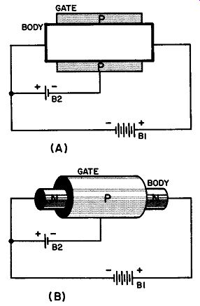
Fig. 710. The field-effect transistor. A cross-section is shown in A.
In B we see how the gate, made of p-type germanium, fits snugly as a
jacket around the n-type germanium.
What we are interested in, though, is control of the current going from the source to the drain. As we increase the reverse biasing between gate and body, current flow from source to drain also decreases, until finally it levels off to a steady value.
Never content to let a condition of status quo exist, suppose we turn our attention once again to the voltage between source and drain, shown as B1 in Fig. 710-B. As we increase this voltage you would expect two things to happen: a) faster current flow and b) more current flow. Electron speed is accelerated, but be yond a certain value of gate voltage, known as the pinch-off voltage, we do not get an increased flow of current through the body from source to drain. This might seem strange until we consider that the gate has surrounded the body with a strong electric field which repels electrons.
The field-effect transistor, complete with input and output, is shown in Fig. 711. The input resistance, because of the reverse biasing supplied by battery B2, is extremely high and is in the order of megohms. This was to be expected, because, as we mentioned earlier, the current flow between gate and body is negligible. The output is a lower impedance, since, even though we have restricted the amount of current flow through the body from source to drain, it is still much greater than between gate and body.
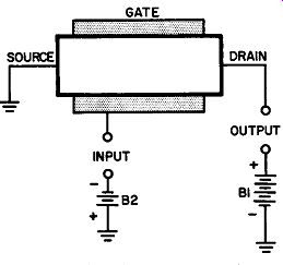
Fig. 711. The field-effect transistor has a high-impedance input, a
lower impedance output.
The field-effect transistor works more like a tube than any other transistor. We can consider the source as the cathode, the drain as the plate and the gate as the control grid. The input and output impedances are like those of a tube. But, while the field-effect unit is a triode transistor, its characteristic curve is somewhat like that of a pentode vacuum tube.
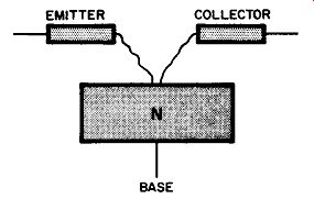
Fig. 712. Point-contact transistor is the forerunner of the junction
type.
The point-contact transistor
Now that we have covered a few (and we mean just a few) of the possible transistor types, it is our sad duty to tell you that we have thus far completely ignored and neglected the honorable ancestor of all transistors--the point-contact. Its glory dimmed by its illustrious offspring, the point-contact may yet come back into its own since it has some remarkable characteristics. It has an alpha greater than 1, and it is adept where a transistor is needed for rapid switching purposes.
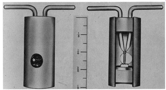
Fig. 713. Exterior and interior views of a point-contact transistor.
(Bell Telephone Laboratories, Inc.)
We have a drawing of the point-contact transistor in Fig. 712 and a photo in Fig. 713. As you can see, we've started with a slice of n-type germanium and have placed two springy metallic points on it. One of these is called the emitter, the other the collector, while the n-type section is the base. A voltage is placed across the emitter and collector leads momentarily, so that a current passes between them. This is believed to form p-type germanium regions in the immediate area around the contacts, thus supplying us with a p-n-p type transistor. In use, the point-contact is biased in the same way as a p-n-p junction type transistor.
It is quite some time since we talked about alpha. Briefly, it is the ratio of collector current to emitter current and for transistors (except the hook transistor and the point contact) is less than I. In other words, collector current is always less than emitter cur rent. In the point contact transistor, collector current is some times as much as twice the emitter current. This might seem a great advantage, but it leads us into a trap. Current flowing through a transistor (uncontrolled) tends to produce more cur-rent. This is current runaway and can destroy a transistor faster than you can reach for a switch to turn off the current.
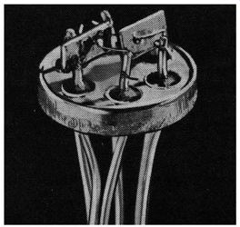
Fig. 714. Interior view of a multi-headed transistor. (Electronic Transistors
Corp.)
Multi-headed transistors
Ever pack a suitcase? With a little ingenuity, planning and some brute force to close the cover, the amount of clothing you can get into a small space is amazing. A similar technique is used in vacuum tubes, ranging all the way from duo-diodes, diode triodes, triode-triodes, right on up to the Compactron--a multiplicity of tubes all within the single glass envelope.
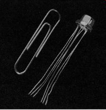
Fig. 715. Multi-headed transistor, shown in actual size. This unit contains
two transistors in one package. (Electronic Transistors Corp.)
Transistors aren't to be outdone by this. Multi-headed transistors can be had in any desired combination. We have an inside view of one of these in Fig. 714. This unit contains two transistors in one package. The two transistors are completely independent of each other, can be used singly or in combination. Each multi headed unit has six leads. You can get an idea of the size of the unit in Fig. 715.
Tandem transistors
In some vacuum tubes certain elements are internally connected; in others, each element is independent. Thus, we can have Fig. 716. The tandem transistor is connected internally.
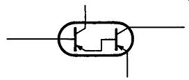
Fig. 716
A suppressor grid internally connected to the cathode, or wired to a pin in the base so we can make any use we want of the suppressor.
The multi-headed transistor is designed for external wiring, but as shown in Fig. 716, we can also have transistors connected internally. The unit in Fig. 716 has the emitter lead of the first transistor wired to the base of the following one. In some tandem units, the collector is the tied-in element, wired to the base of the following transistor. All sorts of combinations are possible but aside from the saving in space, there is no particular advantage in using a tandem transistor instead of two separate units.
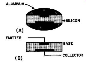
Fig. 717. The evaporation-fused transistor uses aluminum, fused into
the silicon, for the emitter and collector connections.
Germanium and silicon
In an earlier section we brought in a little bit of chemistry for you to examine. At that time we became particularly interested in those elements which had four electrons in their outermost orbit. We have a nice collection of these--carbon, silicon, germanium, tin and lead. Now the order in which we have listed these elements isn't accidental. Carbon has two electron rings, silicon has three, germanium has four, tin has five and lead has six. Thus we started with the lightest element and moved along to the heaviest. Although all of these elements are related in that they have similar outermost electron rings, they do have very definite differences. Consider the two heaviest--tin and lead.
These are metals, nor do you have any doubt that they are. Silicon and germanium, though, aren't really metals, but semimetals. And when we get to carbon we arrive at an element that does not have metallic properties.
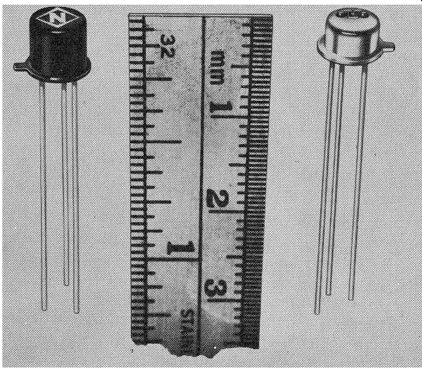
Fig. 718. These silicon mesa transistors are about 3/16 inch long (National
Semiconductor Corp.)
Germanium is the most widely used semimetal or semiconductor. Silicon transistors, though, do have certain characteristics that may make them more desirable. They do not suffer as much from high temperatures as germanium transistors. Also, they have lower leakage currents. Silicon is a much more abundant semi metal than germanium, but it is much more difficult to purify.
1. As in the case of germanium, silicon must be purified and then "doped" with controlled impurities so that we get either p-type or n-type silicon. One type of silicon transistor, known as the silicon alloy or evaporation-fused transistor, is shown in Fig. 717.
In the manufacture of the silicon-alloy transistor, cavities are cut into the silicon wafer. Aluminum is evaporated and allowed to alloy into the surface of the silicon. The result of this process is shown in Fig. 717-A. The excess aluminum is then removed.
The aluminum that remains in the upper and lower cavities forms the emitter and the collector, illustrated in Fig. 717-B.
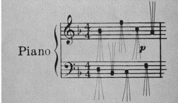
Fig. 719. The transistors shown here in actual size are smaller than
the musical notes they represent. (Raytheon Co.)
1. The nonmetal carbon, and the semimetal silicon, as elements or as compounds form all living material. Practically all of the earth's minerals are accounted for by just these two elements.
Transistor dimensions
Transistors, other than those used for work as power amplifiers, are well-known for their smallness. Typical units are shown in the photograph, Fig. 718. But small as they are, even tinier units are needed for special applications where all space is at a very high premium. This could include missile units or computers using tremendous numbers of transistors, or in hearing aids. Fig. 719 shows some of these, representing the notes on a musical staff.
Actually, these subminiature transistors, intended for hearing-aid use, are smaller than the musical notes they will amplify.
At this point we must be careful not to fall into the trap of thinking that reduction in size means an increase in the alpha cutoff frequency. With vacuum tubes, one way of raising the operating frequency was to bring the cathode closer to the plate, and since the tube envelope accommodated this space shrinkage, the result was a smaller tube. This situation is not analogous in the case of transistors. In some cases, subminiature transistors have a lower alpha cutoff frequency than their bigger brothers.
A representative subminiature might have a height of 0.160 inch compared to 0.260 inch for the more common type. This is a difference of only a tenth of an inch, but think of it in terms of percentage and you will see that the decrease in size is quite astonishing. But this doesn't mean that the end has been reached.
The hearing-aid transistors in Fig. 719 are less than 0.1 inch in height, while some are down to 0.05.
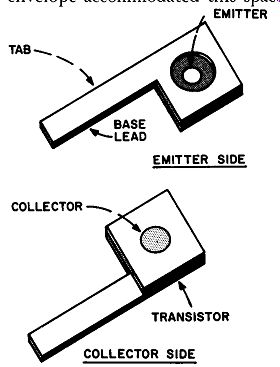
Fig. 720. The transistor is mounted on a tab which forms the lead for
the base.
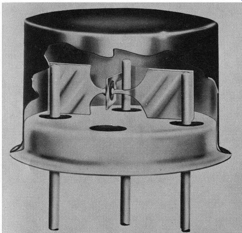
Fig. 721. Interior view of an alloyed-junction transistor. A pair of "bow
ties" connects the emitter and collector to their external leads.
The center, or base lead, is connected to the body of the transistor
by a tab. (Raytheon Co.)
Transistor manufacture
The first step, and probably the most important in the manufacture of transistors of all types, is refining the semiconductor material. The refining process is carried to the point where the semiconductor is almost 100 percent pure. The silicon or germanium is then melted. While the semiconductor is in this molten state, either donor or acceptor impurities are added. The type of impurity will determine whether we will have n-type or p-type semiconductor.
At this time, a small bit of crystalline material known as the seed is dipped into the melt and is then withdrawn slowly. The effect of the seed is to trigger the crystalline formation of the semiconductor. This crystalline formation, though, is not in the direction of millions of tiny crystals, but rather more like that of a single, large crystal.
Did you ever watch a salami being sliced by a machine? That's our next step, but the cutting of the semiconductor crystal is carried on in sanitary surroundings that no delicatessen could duplicate. Each thin semiconductor wafer is then cut into tiny chips. These tiny bits of semiconductor crystal are our transistors.
In the manufacture of the most common type of transistor, the junction transistor, tiny dots of indium, aluminum or antimony are alloyed to the surfaces of the semiconductor.
Our transistor is now completed, but we must somehow make connections to the emitter, collector and base. As a start, we mount the transistor on a metal tab, as shown in Fig. 720. This tab now forms our connection to the base of the transistor. As you can see in the drawing, a hole is cut in the tab to permit access to the dots of indium. The unit is now mounted in its housing or package and is ready for testing.
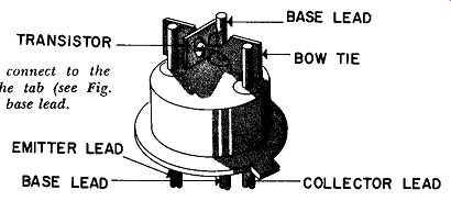
Fig. 722. The bow ties connect to the emitter and collector. The tab
(see Fig. 720) connects to the base lead.
In Fig 721 we have a cutaway photo of an alloyed-junction transistor. As you can see, this resembles the drawing in Fig. 722.
However, various manufacturers all have their own techniques.
Thus, a similar transistor in Fig. 723 shows wires connected to the indium dots. These wires help support the transistor and also make connections to the external emitter and collector leads. No tab is used in this particular construction with the exception of a small rectangular block from the body of the semiconductor to the base lead.
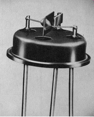
Fig. 723. In this alloyed-junction transistor, a pair of wires is used
to help support the transistor and to connect to the emitter and collector.
Note the circular holes cut in the "package" to permit the
external leads to come through to the emitter, base and collector. (Raytheon
Co.)
Power transistors
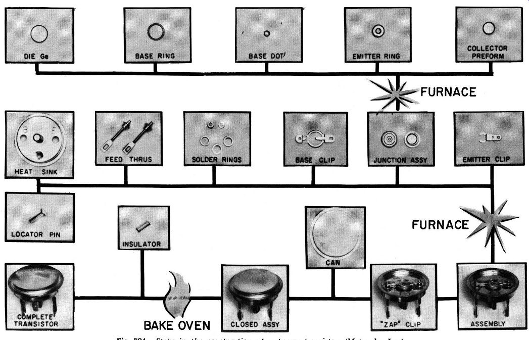
Fig. 724. Steps in the construction of a power transistor (Motorola,
Inc.)
Power transistors, as their name implies, represent the final link between the load and the signal. In the case of a radio receiver the load is the speaker and since the voice-coil type of speaker is a current-operated device, it must be driven by a transistor capable of delivering audio power. Power transistors are no different than ordinary transistors, except they are specially de signed to handle large values of current. Thus, in the case of ordinary amplifying transistors we are accustomed to currents in microamperes and milliamperes; for power units we can have de collector currents of 10, 20 amperes or more. These large currents raise immediate problems, for where we have a high current there is always the pressing question of an IR drop. When currents are measured in amperes, just a small amount of resistance causes a voltage loss. Of equal concern is the fact large amounts of heat result from PR losses. Since the power to be dissipated (in the form of heat) varies as the square of the current, heat sinks must invariably accompany power transistors. Thus, if we consider the movement of a moderate amount of current such as 10 amperes through a 1-ohm resistor, we would have (based on the formula: W = FR) 10 X 10 X 1 or 100 watts. Now this may not sound like much, but try touching a 100-watt electric-light bulb after it has been on for a few minutes and you will get the skin-blistering idea.
Number of leads
In Fig 724 on the we have the step-by-step processes used in the manufacture of power transistors. The heat sink is an integral part of the transistor assembly, but in itself this is often inadequate. The metal chassis on which the transistor is mounted helps dissipate the heat, or specially-designed separate heat sinks are provided. These are often corrugated or ribbed to supply the maximum amount of radiating surface.
Not only are power transistors much heavier and larger than ordinary amplifying transistors, but instead of having three connecting leads most have just two. These leads are for the base and the emitter. The collector of the power transistor is mechanically and electrically connected to the metal shell of the unit. Incidentally, as you might expect, while the majority of amplifying transistors (other than power transistors) have three leads, there are some that have four. A transistor of this type is the post-alloy diffusion transistor (abbreviated as PADT) which has an extra lead connected to the case.
Mounting transistors Since transistors (other than power types) are so extremely small and light, mounting them is no more of a problem than mounting a quarter-watt resistor. Just keep in mind that transistors aren't too partial to the heat of a soldering iron and there should be some sort of thermal shunt on the transistor lead, between the tip of the soldering iron and the transistor proper, to bypass the heat of the iron. You can avoid the need for a thermal shunt by using a clean, well-tinned iron and soldering with the correct melting point solder. Transistors are not affected by the rather substantial magnetic field surrounding a soldering gun or the smaller field around the usual soldering iron.
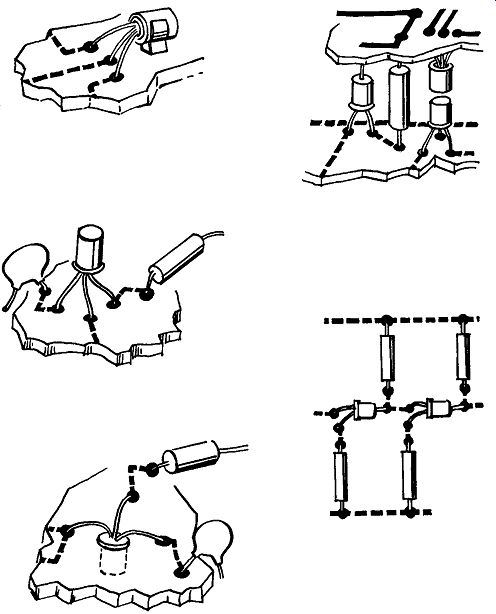
Fig. 725. These are some transistor mounting techniques. Transistors
can be placed in any position. (Raytheon Co.)
Sockets
Sockets are sometimes used for transistors, but since the life expectancy of a transistor is equal to or better than most other components, the transistors can be soldered directly into place.
Unlike tubes, transistors can be soldered in any position. They can be mounted vertically, horizontally, below, above or between printed boards, as shown in Fig. 725. Transistors can be connected so that they sit on their leads, or hang from them.
Circuit packaging
When you service a radio or television receiver you do so with the idea of finding the one component that is defective. Granted that sometimes the trouble is caused by more than one defective part, the fact remains that servicing consists first in localizing the difficulty and then in isolating the troublemaker.
For equipment used in industry and in military applications this approach is time-consuming. It can also be expensive, since the down time of a machine such as a computer can cost far more than any amount of servicing. For this reason a circuit that does not work properly is completely replaced. Granted that a half dozen or so good parts might surround one weak component, this is still faster and far more economical than to institute a search for and replacement of an individual resistor, capacitor, transistor, etc.
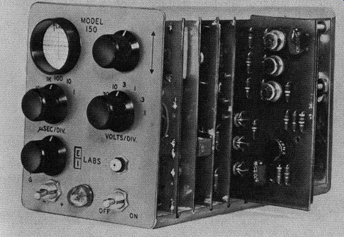
--------- Plug-in modules often contain complete stages. It is a
form of construction that supplies a very high component packaging density.
In the instrument shown above, components are mounted on boards which
slide into grooves. Connections are made through special connectors on
the inside edge of each of the boards. [El Labs]
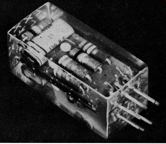
Fig. 726. Packaged transistor
circuit. (Bell Telephone Laboratories, Inc.)
Earlier we have a number of packaged circuits. These can be used in original design applications or as replacements. A complete electronic device can be built of these blocks and can be repaired by simple substitution. The components are connected and are then encapsulated and potted into a variety of packages - tubular, rectangular, bathtub shape, etc. Connecting leads are brought out to a 9-pin standard plug-in base, octal and subminiature in-line base, a 7-pin standard base, or with pig-tail leads or pin terminals. Replacement is as simple and as easy as replacing a tube. Fig. 726 shows an experimental model of a transistor amplifier for telephone switching circuits. All components of this miniature plug-in type device, including the beaded-junction transistors, are compactly embedded in Lucite. The model is about 1 %-inches long.
Other transistor types
The transistors we told you about earlier in this section are just a few of the many different types. There are so many of them now, and so many constantly being developed, that a book could be written just describing them. And each new type that is produced may have as many as a half-dozen different names depending on the manufacturing techniques being used. Little purpose would be served in listing them all here, for the list would be out of date on publication.
There is one more item we should discuss and that is that transistors represent just one branch on the semiconductor tree. There are many types of semiconductor devices. Among the best known of these are the diodes. Transistors are the most glamorous, have been the most publicized, and are the only types of semiconductors described in this guide.
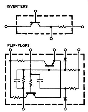
-------- Inverters are well named since they are used to do just
that to an electrical signal.
Basically amplifiers, they have no gain. The out put has .the same amplitude but opposite polarity of the input.
Flip-flops, equally well named, come in many varieties. Some are used for counting, others for pulse shaping or pulse generating.
Amplifiers need no further explanation as to their application. They may be used before, after or between any of the modules.
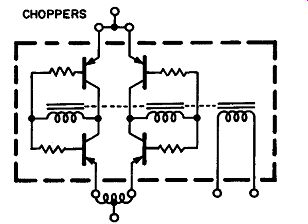
----------In the chopper, the three-winding transformer, indicated by
the dotted line, feeds a pulse to the transistor bases. The polarity
of the pulse causes one or the other of each transistor pair to conduct.
These modules are plugged in to connection boards for rapid setup of
complex control systems or small computers.
-----------Modules are taking the place of much electronic wiring. Some modules are no bigger than a transistor alone. Computers and data control equipment may consist of a dozen module types repeated several hundred times. One group of modules is logic circuits which have multiple in puts. A signal or the lack of a signal at one or more of these inputs will cause or prevent an output signal to the next stage which may be an other logic module, an inverter, a flip-flop of one of many varieties or a relay or readout device.
Transistors are probably best known to you through their use in radio receivers. But the radio receiver circuits we covered in earlier sections represent just the beginning, not the end of the tremendous number of ways in which transistors can be used in circuits. In our next section we are going to examine some of them.
QUIZ
1. What is transit time? How does it affect transistor operation?
2. What is alpha cutoff frequency?
3. How does the tetrode transistor differ from the triode transistor?
4. How does a surface-barrier transistor overcome the problem of transit time?
5. What are the differences between a micro-alloy transistor and a MADT type?
6. Describe the major characteristics of germanium and silicon as a semiconductor.
7. What characteristic does the hook transistor have in common with the point contact transistor?
8. What are modules?