AMAZON multi-meters discounts AMAZON oscilloscope discounts
IC chips can be divided broadly into two main categories-complete circuits or subcircuits with internal connections, and arrays. The latter consist of a number of individual components connected only to the external pins of the IC chips, or, in some cases, two (or possibly more) internally connected components together with individual components.
For example, Darlington pairs of transistors included in an array would be connected within the chip.
An example of a simple IC array is shown in Fig. 14-1. It consists of three transistors (two interconnected), two types of diodes, and a Zener diode.
Circuits are commonly designed around IC arrays, in this case, a voltage regulator using two of the transistors, the SCR diode, and the Zener diode. This circuit design is shown in Fig. 14-2. The components to be utilized which are contained in the IC are enclosed in the dashed outline, TR1, TR2, D2 and D3. The other components in the chip (D1 and TR3) are not required. Resistors R1, R2, R3, and R4 and a capacitor C, are all discrete components connected externally.
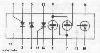
Fig. 14-1. CA3097E IC array (schematic).
Figure 14-3 shows this circuit redrawn as a physical diagram, relating the connection of external components to the chip. Pins in this diagram are shown in the actual physical order they appear on the integrated circuit.
For ease of reading, pins are shown numbered and enclosed in circles rather than numbered tags.
On circuit drawings, pin numbers may be shown circled or not. For clarity, the integrated circuit is drawn much larger in proportion to the external components.
Note that the arrangement of the leads does not necessarily follow the schematic diagram (Fig. 14-1) where the pins are in random order to clarify connections to internal components.
The actual pin arrangement on ICs follows a logical order reading around the chip.
Schematic diagrams may or may not follow in the same order (usually not). Connections for completing the circuit of Fig. 14-3 are:
Leads 1, 2, and 3 are ignored as D1 is not used.
Lead 4 connects one side of the Zener diode to the common ground line.
Lead 5 to Lead 13, connects the Zener diode to the correct side of the SCR (diode).
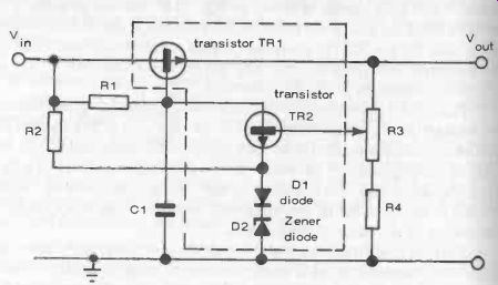
Fig. 14-2. Voltage -regulator circuit using CA3097E array.
Leads 11 and 12 connect together (as the SCR is worked as a simple diode in this circuit, and the gate connection is not required).
Now to pick up the transistor connections; The base of TR1 (15) connects to the external resistor R1, and the collector lead (14) to the other side of R1, which is also the input point for the circuit. The emitter lead (16) connects to output.
TR2 and TR3 in the chip are interconnected, but only one of these transistors is required. Connecting lead (6) to (9) shorts out TR2, which is not wanted.
Connecting the emitter lead (8) of TR3 to 11-12 (already joined), the collector lead (9) to (6), and the base lead (7) to the center tap of the external potentiometer R3 connects TR3 into the circuit.
It only remains for the external component connections to be completed.
These are:
R2 to lead (14) and lead (12).
Capacitor C to lead (6) and ground point.
Lead (10) on the IC is also the substrate or ground point of the IC, so should also be connected to the common ground line.
One end of the potentiometer R3 to the top (output) line.
The other end of the potentiometer to R4.
The other end of R4 to the bottom common ground line.
It will be appreciated from this circuit, and a study of others, that the number of components in an array may not be used in a particular circuit, but the cost of the single IC can often be less than that of the equivalent transistors or diodes ordered separately and used individually to complete the same circuit.
A circuit using the IC will also be more compact and generally easier to construct.
A little study sometimes shows where further savings are possible.
Figure 14-4 for example, shows a voltage doubler circuit for a 1 -kHz square -wave input signal, based on a CA3096E IC array which contains 5 transistors. Only three of these transistors are used in this particular circuit, leaving two "spare."
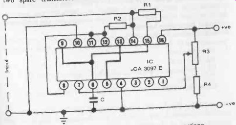
Fig. 14-3. Complete voltage -regulator circuit with wiring connections.
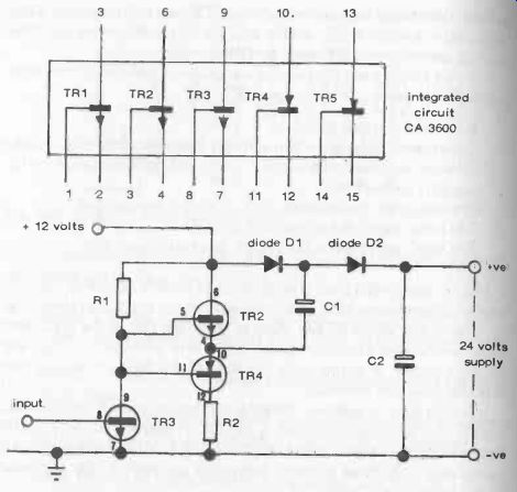
Fig. 14-4. Schematic diagram of CA3600 array (top) and voltage-doubler circuit
(bottom).
The circuit calls for two diodes, D1 and D2 (as well as three resistors and two capacitors), to be added as discrete components.
Transistors can also be worked as diodes (by neglecting the collector lead), and so the functions of D1 and D2 could be performed by the two "spare" transistors in the array (thus using up all its components).
Alternatively, since the current needs a square wave input signal, the two "spare" transistors could be used in a multivibrator circuit to provide this input, in this case using discrete components for D1 and D2. Since diodes are cheaper than transistors, this is a more economic way of using all the components in the original array.
The fact that popular ICs are quite cheap means that is seldom worthwhile going to elaborate methods of trying to use all the components available in an array, unless such utilization is fairly obvious, as above.
Using only part of an array can still show savings over the purchase of individual components for many circuits.
Component values for Fig. 14-4 are:
R1 = 10 ohms
R2 = 1 k-ohm
C1 = 2.5 uF
C2 = 2.5 µF
Diodes:
D1 an D2.