AMAZON multi-meters discounts AMAZON oscilloscope discounts
An amplifier can be defined as a device, or circuit, providing multiplication of a signal, i.e., an output signal greater than the input signal.
It is a characteristic of a transistor that it works as an amplifier of signals. In the most widely used mode of connection of transistors for such duties, with input and output circuits both connected to the emitter (common -emitter mode), the degree of amplification or current gain is called the "beta" (Beta) of the transistor. This is given as h_FE (or static forward current ratio) in transistor characteristics data.
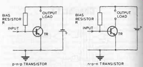
Fig. 17-1. Basic amplifier circuit.
BASIC AMPLIFIER CIRCUITS
A basic transistor amplifier circuit is very simple-and is identical for a PNP or NPN transistor, except for the battery polarity, see Fig. 17-1.
Virtually any low -power of transistor can be used in this circuit. The bias resistor (R) must have a value providing a collector current not exceeding the maximum specified rating for the transistor used, the actual current flowing in the collector circuit also being influenced by the voltage of the battery.
Knowing the transistor characteristics, a suitable value for R in Fig. 17-1 can be calculated as follows:
R = gain x battery voltage collector current battery voltage
= hFE x
where I is equal to, or preferably less than, the specification figure for I max. Example: A small signal transistor has the values of I max = 250 mA, c and h_ = 30 to 90. Taking the maximum gain, and 175 mA as a "safe" working figure for the collector current:
R = 90 x -9
0.175
= 4,630 a
A suitable (preferred -value) resistor would thus be 4.7 k.
Figure 17-2 shows the complete circuit for an elementary of amplifier of this type, coupled to the "front end" of a basic crystal set. The detector (output) is coupled to the amplifier via capacitor C2, a suitable value for which would be 10 uF or higher (20, 25, 30, 40, or 50 µF): Capacitor C1 (0.001µF) may not be necessary. The output load in the collector circuit is formed by high -impedance phones.
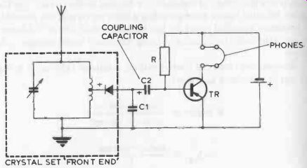
Fig. 17-2. Crystal set with one stage of amplification.
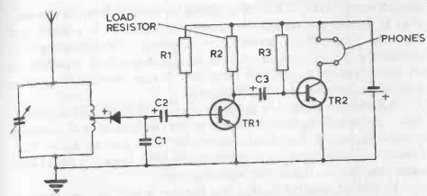
Fig. 17-3. Crystal set with two stages of amplification. Component values
matching 0071, 0072 or near equivalent for TR1 and TR2:
Note that the polarity of the battery used to power this circuit is R1, 6.8 or 10 k R2, 4.7 k R3, 22 k
Battery voltage 6 to 9 V.
C1, 0.001 uF C2, 8 or 10 uF C3, 8 or 10 µF important as far as the transistor connections is concerned and also because of the connections to the diode and C2 (which will normally need to be an electrolytic type to provide the high-capacitance value required).
With an NPN transistor, the battery polarity would be reversed, as would be the diode and electrolytic-capacitor connections.
The same type of circuit can be used to provide additional amplification, if required, simply by adding another amplifier stage (Fig. 17-3).
The second amplifier stage can be identical to the first, or based on a higher-power transistor taking the output present and providing even greater gain.
The load in the output (collector) of the first amplifier stage is provided by a resistor (R2) (which should be about the same value as the phone resistance, 3.3 to 4.7 k). The two stages are coupled by a capacitor (C3). Value of R3 depends on the second transistor used, and may be anything from 130 to 1 k ohm. Capacitors C2 and C3 can be 10µF or larger.
A more compact two-stage amplifier circuit is shown in Fig. 17-4.
This may prove capable of operating a small loudspeaker direct, although the current drain will be quite high.
Alternatively, three or four stages of amplification using low -power transistors, following a basic "front end" crystal set, should provide enough power to drive a small loudspeaker at the final output, through a suitable step-down transformer to provide an impedance match.
Simple amplifier circuits of this type have the important limitation that performance of the transistor(s) will tend to vary with temperature. There Is also the possibility of "thermal runaway" developing, which can destroy the transistors, because, as the external temperature increases the collector current also tends to increase, which in turn causes a further increase in junction temperature. The effect is cumulative and goes from bad to worse, even to the point of ruining the transistor completely. It is possible to overcome this trouble by arranging for the circuit to be self-biasing or dc stabilized so that a constant collector current is provided, regardless of transistor type or temperature variations. In other words, the working point of the collector circuit is stabilized.
A further advantage of a stabilized circuit is that it makes the performance of the amplifier less dependent on the characteristics of individual transistors, which can differ appreciably even for the same type, Capacitor-coupling between stages should be used, since this makes each stage independent, rather than interdependent.
To achieve this, the original bias resistor is split into two separate values, R1 and R2 (see Fig. 17-5). A further bias resistor (R3) is applied directly to the emitter, in parallel with a capacitor (C) to act as a by-pass for of currents.
A receiver design incorporating two stages of amplification with stabilized circuits, following a conventional front end is shown in Fig. 17-6.
This, in fact, is about as far as it is practical to go with such a basic circuit because, although additional complete stages will provide more gain and greater final output power, any deficiency in the circuit will also be aggravated--notably lack of sensitivity and selectivity in the front end.
The amplifier stages also provide a convenient point to insert a volume control into the receiver circuit. This takes the form of a potentiometer which can replace one of the bias resistors, or be placed in series with the flow of the current after the first stage of amplification, Fig. 17-7. This will introduce minimum distortion over the volume control range.
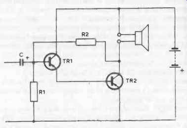
Fig. 17-4. Amplifier for loudspeaker output.
Components:
TR1, OC44
TR2, AD140 C, 8 or 10 AF
Loudspeaker, 8 ohm
R1, 6.8 k
R2, 33 k
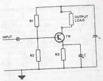
Fig. 17-5. Transistor amplifier stage with stabilized bias. Typical values
for low/medium-power transistors:
R1, 22 k
R2, 10 k
R3, 1k
C, 8 or 10 uF
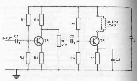
Fig. 17-7. Two-stage amplifier with volume control.
Amplifier Output Stages
Single transistor outputs
work in "Class -A" operation, which means that the values of bias and signal voltage applied to the transistor ensure
that collector current always flows. Figure 17-8 shows a basic Class -A
output circuit incorporating
transformer coupling to a loudspeaker.
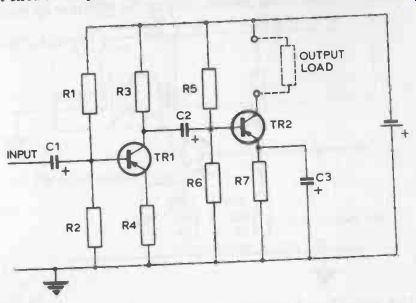
Fig. 17-6. Two -stage amplifier circuit.
A more economic way of producing satisfactory output power is to use a single transistor driver working a complementary pair of transistors (an NPN and a PNP selected with matched characteristics) in push-pull configuration. The output power obtained from a pair of transistors in push-pull is considerably more than double the power obtained from a single transistor of the same type.
With "Class B" operation, the transistors are biased to nearly cut-off, so that only a marginal current flows under "quiet" conditions. Push-pull outputs may, however, also be designed for "Class-AB" operation, with rather higher current drains.
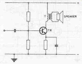
Fig. 17-8. Basic Class-A amplifier circuit.
Basically, distortion is lowest with Class-A operation, while Class -B operation provides the lowest current drain but introduces the possibility of crossover distortion being present. This can be overcome by applying a slight forward bias to each transistor. Class-AB offers a compromise between the two.
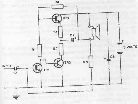
Fig. 17-9. Push-pull amplifier.
Components:
TR1, BC109 TR2, AC1281
Complementary pair
TR3, AC176
Loudspeaker, 3 11 or 8 R1, 68 R2, 1 R3, 1 R4, 1 k R5, 1 k C1, 5µF C2, 250 uF C3, 50 uF
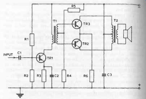
Fig. 17-10. Push-pull amplifier with transformer coupling. TR1 is the driver;
TR2, TR3, AD140 or AD149. Typical component values:
R1, R2 to match
TR1 (depending on type used)
R3, 1k
C2, 50 µF
R4, 100
C3, 50 µF or 80 µF R5, 4.7 k
T1, coupling transformer
R6, 10
T2, output transformer
Two types of basic push-pull output circuits are shown in Figs. 17-9 and 17-10, one with direct coupling and the other using transformer coupling, both interstage (between driver and push-pull input) and to the loudspeaker. The coupling transformer can provide voltage step-up.
An output transformer, on the other hand, is invariably a step-down type to adjust the loudspeaker impedance to the required output impedance. Both types of circuits have their advantages and disadvantages, although for simpler receivers, all-transistor circuits are usually preferred.
Much also depends on the requirements of the receiver. To operate a small loudspeaker successfully, an audio power output of 5 mA or better is required (higher still for larger speakers, of course). At the other extreme, about 10 µA represents, for most people, the threshold of audibility in high-impedance phones; and 0.1 mA is a normal minimum for comfortable listening and ready identification of sounds in headphones. For easy listening with high-impedance phones, an audio output power of up to 0.5 mA is desirable. Higher signal levels will tend to "swamp" headphones but can, of course, be reduced by a volume control. Typical characteristics of head phones, earpieces, and loudspeakers are:
Headphones
High-impedance type, dc resistance 2,000-4,000 ohms, typical impedance 10,000 ohms (at 1 kHz).
Low-impedance types, (i) dc resistance 15 ohms, typical impedance 80 ohms (at 1 kHz); (ii) dc resistance 80 ohms, typical impedance 120 ohms (at 1 kHz).
Earpieces
High -impedance types, (i) dc resistance 2,000 ohms, typical impedance 15 ohms (at 1 kHz); (ii) dc resistance 14 ohms, typical impedance 60 ohms (at 1 kHz); (iii) dc resistance 60 ohms, typical impedance 250 ohms (at 1 kHz).
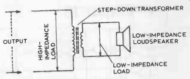
Fig. 17-11. Using an output transformer to balance the load.
Loudspeakers
Typical dc resistance 3 ohms, typical impedance 8-16 ohms.
It will be obvious from a study of these figures that low-impedance phones, a low-impedance earpiece, or a loudspeaker will be a mismatch for coupling to an output requiring a high-impedance load (as in the case of most of the simple all-transistor output circuits).
To employ low-impedance phones, earpiece, or a loudspeaker with an output requiring a high-impedance load, a matching step-down transformer (output transformer) must be used. The primary of the transformer then provides the required output load, indirectly coupled to the secondary to which is connected the low-impedance phones or speaker, Fig. 17-11. The turns ratio required from the transformer is easily calculated as:
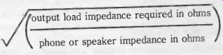
output load impedance required in ohms ( phone or speaker impedance in ohms
Some typical transformer ratios and their suitability for matching are:
Ratio 41:1
Listening device
Speaker
Equivalent output load impedance ohms 29,000 35:1 4-ohm earpiece 20, 000 30:1
Speaker 10, 000 18:1 14-ohm earpiece 20,000 14:1 15-ohm earpiece 20,000 9:1 60-ohm earpiece 20,000 5:1 80-ohm headphones 20,000