AMAZON multi-meters discounts AMAZON oscilloscope discounts
Table of Contents:
- Introduction
- Junction Transistors
- NPN Transistors
- PNP Transistors
- Alloy-Junction Transistors
- Review
- Self-Test Questions
- Field-Effect Transistors
- Junction-Gate Field-Effect Transistors
- Insulated-Gate Field-Effect Transistors
- Review
- Self-Test Questions
- Answers to Self-Test Questions
- Lesson Questions
-------------------
Lesson Objective:
In this lesson you will...
• Learn how transistors are manufactured, and how they work.
• Discover the different types of junction transistors.
• Investigate some special types of junction transistors.
• Learn the operation of field-effect transistors.
• Study the two basic types of field-effect transistors.
INTRODUCTION
Invented in 1948, transistors have replaced vacuum tubes in all but a few, special cases. They were developed in the Bell Telephone Laboratories for use as amplifiers of voice signals. The first transistors had very limited capabilities and could be used only at audio frequencies. Transistors have improved over the years, and today they outperform vacuum tubes in every application except video displays.
Transistors have many advantages over vacuum tubes. Tubes have cathodes which must be heated to give off electrons. The energy that heats the cathode does not contribute to the signal amplification, and therefore, is considered wasteful. In operation, vacuum tubes get very hot and this heat spreads to other parts in the equipment, contributing to part failure. Transistors consume much less energy and produce less heat.
Transistors are also smaller and more rugged than vacuum tubes. A sharp blow to a vacuum tube could break the glass envelope or cause the tube to short, making it useless. A transistor is a solid device, so a sharp blow is not likely to cause a problem.
You will find transistors in radio receivers, telephone receivers, video cassette recorders, transmitters, and all types of computers. Many of the devices we accept as commonplace today would not exist if it were not for transistors.
The transistor is very important in electronic equipment. It is essential that you understand how it works. This lesson is probably the most important one so far. If there is something you do not understand after the first reading, read that section over until the subject is clear. If you still need assistance, take advantage of the NRI consultation service and write to us. We'll be glad to help you.
---------------
JUNCTION TRANSISTORS
In the preceding lesson you studied diodes. A diode is a two-element device. A transistor is a three-element device. The junction-transistor is the most widely used type, so you will study it first.
Early transistors were made of germanium, but most modern transistors are silicon. In our discussion we'll be talking about silicon transistors, but germanium transistors work in basically the same way.
The two-junction transistor is made from a single crystal having three regions. The center region is made of either n-type or p-type material. The two end regions are made of the opposite type material. Figure 1(A) shows one type of transistor where the center region is made of n-type material. The center region is called the base. At one end is the emitter, and at the other end is the collector. Both ends are made of p-type material. This type of transistor is called a PNP transistor.
Figure 1(B) shows another transistor where the base is made of p-type material and the emitter and collector are made of n-type material. This type of transistor is called an NPN transistor.
Figure 1 also shows the schematic symbols used to represent both types of transistors.
Notice that in the PNP type, the arrow on the emitter points toward the base, while in the NPN transistor, the arrow on the emitter points away from the base. It is important that you remember the names of the three parts of the transistor, as well as the schematic symbols used for PNP and NPN transistors.
In some electronic equipment, all the transistors are either NPN or PNP transistors. In other equipment, both types are used. The NPN transistor is the more widely used of the two; and it is also easier to understand how it operates. We'll discuss this type first.
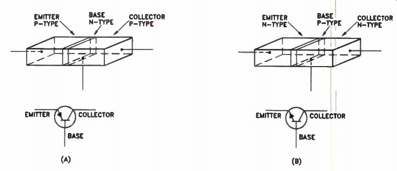
Figure 1. (A) A PNP junction transistor and its schematic symbol. (B)
An NPN junction transistor and its schematic symbol.
NPN Transistors
The junctions of a junction transistor act just like the junctions in a junction diode. Between the emitter and base of the transistor, shown in Fig.2(A), there is a junction. Electrons diffuse from the emitter across the junction into the base of the transistor. When an electron leaves an atom in the emitter, it leaves a hole behind, creating a positive ion. At the same time, an electron moving into a hole in an atom in the base region creates a negative ion. A positive charge builds up on the emitter side of the junction and a negative charge builds up on the base. These charges prevent further diffusion of holes and electrons across the junction.
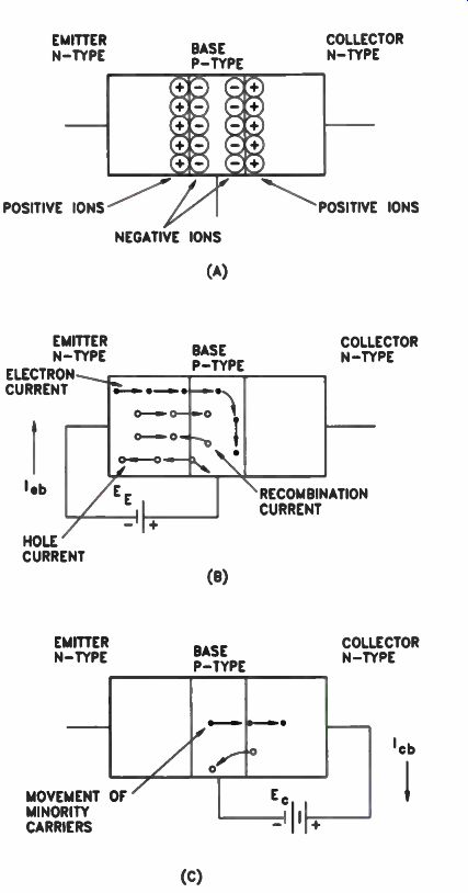
Figure 2. (A) The formation of ions at the junctions of an NPN transistor.
(B) The current flow in the emitter-base circuit, and (C) in the collector-base
circuit.
Meanwhile, the same thing happens at the junction between the base and the collector. Electrons diffuse across the junction into the base region, and holes diffuse across the junction into the collector, building up a negative charge on the base side and a positive charge on the collector. Once established, these charges prevent any further diffusion of electrons and holes across the junction.
Look at what happens when a forward bias is placed across the emitter-base junction, as shown in Fig.2(B). Notice that the negative terminal of the battery connects to the emitter and the positive terminal of the battery connects to the base, which places a forward bias across the emitter-base junction.
The negative potential applied to the emitter forces electrons toward the junction, and at tracts holes away from the junction. Both actions tend to neutralize the positively charged ions on the emitter side of the junction. The positive terminal of the battery attracts electrons away from the base side of the junction, while it repels holes toward it at the same time. These two actions tend to neutralize the charge on the base side of the junction.
With the weakening of the barrier potential at the junction, electrons flow from the negative side of the battery through the emitter, across the junction, into the base, and from the base to the positive terminal of the battery At the same time, the positive terminal pulls electrons from the base, forming holes. These holes are repelled across the junction, through the emitter toward the end connected to the negative terminal of the battery In the emitter, holes pick up electrons and disappear. Thus, we have a current flow through the emitter-base circuit as shown in Fig.2(B). Not all the electrons crossing the emitter-base junction reach the positive terminal of the battery Some of them fill holes in the p-type base material. Similarly, not all the holes crossing from the base into the emitter reach the negative terminal of the battery. Some are filled by electrons in the emitter. This current, made up of electrons that fill holes in the base and holes that are filled by electrons in the emitter, is called a recombination current and the transistor is designed to keep this current as low as possible because it serves no useful purpose. To maximize transistor efficiency, we want the holes and electrons crossing the junction to reach the ends of the crystal.
Now let's see what happens when a reverse bias is placed across the base-collector junction by connecting the negative terminal of a battery to the base, and the positive terminal to the collector, as shown in Fig.2(C). This increases the negative charge on the base of the junction and the positive charge on the collector side of the junction, so the potential barrier across the junction increases. This prevents current flow across the base-collector junction due to majority carriers.
At the same time, electrons, which are minority carriers in the base, break loose from their atoms and from the depletion layer on the base side of the junction. These electrons are attracted by the positive potential applied to the collector. They cross the junction and flow through the collector to the terminal connected to the positive side of the battery, as shown in Fig.2(C).
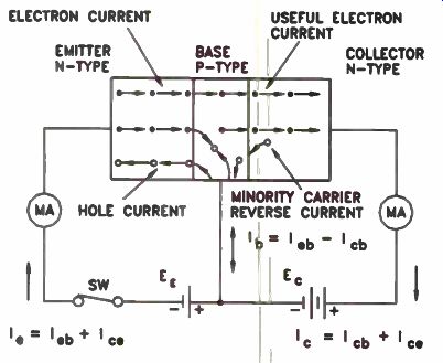
Figure 3. Current flow and carrier movement in an NPN junction transistor.
Simultaneously, holes formed in the depletion layer on the collector side of the junction move toward the negative terminal of the battery, cross the junction, and flow over into the base and toward the negative terminal of the battery.
Here they pick up electrons and disappear. Thus, we have a current flow in the base-collector circuit due to the minority carriers.
Now look at what happens when bias voltages are applied across both junctions of the NPN transistor, as shown in Fig.3. Considering first the emitter-base circuit, we have electrons flowing from the negative terminal of the battery, through the n-type emitter, across the junction and into the base. Some electrons reaching the base recombine with holes. However, most electrons reaching the base are attracted to the positive potential applied to the collector and flow through the base, across the positive terminal of the battery.
At the same time, the positive potential applied to the p-type base pulls electrons out of the crystal, producing holes. These holes cross the junction into the emitter, drawn by the applied negative voltage. These holes flow through the emitter to the end connected to the battery, where they pick up electrons and disappear.
In the base-collector circuit, a reverse current flows due to the minority carriers. Holes appearing in the collector side of the depletion layer cross the junction into the base and flow toward the negative terminal of the battery, biasing the base-collector junction. Electrons in the depletion layer on the base side of the junction are attracted toward the positive potential applied to the collector. They cross the junction and flow toward the positive terminal of the battery connected between the base and the collector.
With all these currents flowing, the most important, useful current flow is that of electrons from the emitter, through the base, and to the collector. Since this is the useful current, we are interested in making it as large as possible in comparison to the other currents. Recombination current is kept as low as possible by adding more donor atoms to the emitter than acceptor atoms to the base. In this way, there will be more free electrons in the emitter than there will be holes in the base, so the recombination current will be quite small. In a good transistor, over 95% of the electrons that cross the emitter-base junction will flow to the collector.
PNP Transistors
Now let's see how the PNP transistor functions.
In this transistor the emitter and the collector are both made of p-type material and the base is made of n-type material. First, let's consider what happens at the two junctions before any voltages are applied to the transistor.
At the junctions, holes from the p-type emitter section and the p-type collector section diffuse across the junctions into the base. The holes diffusing into the base place a positive charge on the atoms near the junctions. At the same time, electrons from the n-type base diffuse across the junctions into both the emitter and collector.
These electrons diffusing from the base into the emitter, on one side of the base, and the collector, on the other side of the base, place a negative charge on the atoms on the emitter and collector sides of the junctions. These charged atoms, or ions, will repel the electrons and holes from the region of the junction to prevent any further diffusion across the junctions. Thus we will have two depletion layers formed, as shown in Fig.4(A) on the next page.
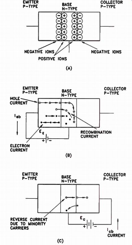
Figure 4. (A) The formation of ions at the junction of a PNP transistor.
(6) The current flow in the emitter-base circuit, and (C) in the collector-base.
Before going any further, you should compare Fig.2(A), which shows the depletion areas in an NPN transistor, with Fig.4(A), which shows the depletion areas in a PNP transistor. Notice that the depletion areas have opposite polarities. In the NPN transistor, at the emitter-base junction, there are positive ions on the emitter side of the junction and negative ions on the base side of the junction. With the PNP transistor, there are exactly the opposite: the negative ions are on the emitter side of the junction and the positive ions are on the base side of the junction.
Notice that the polarity of the depletion layers in the base-collector junctions is also reversed.
In the NPN transistor there are negative ions on the base side of the junction and positive ions on the collector side. In the PNP transistor, on the other hand, there are positive ions on the base side of the junction and negative ions on the collector side of the junction.
Getting back to the PNP transistor, when a forward bias is placed between the emitter and the base, an arrangement is formed like that shown in Fig.4(B). Here the positive voltage applied to the end of the p-type emitter repels holes toward the junction. These holes tend to neutralize the negatively charged ions on the emitter side of the junction. The holes are formed at the end of the p-type section by electrons attracted out by the positive potential applied to this section. At the same time, the positive potential applied to the emitter attracts the electrons that have given the ions on the p-side of the junction their negative charge. This also weakens the negative charge on the emitter side of the junction.
At the base, the holes are attracted toward the negative terminal of the battery, while the electrons are pushed toward the depletion layer.
The pulling of holes away from the depletion area and the pushing of electrons into it tend to neutralize the charge on the base side of the junction. The net effect of biasing in the forward direction is to neutralize the charges on each side of the junction and to allow current flow across the junction. Current flow is by majority carriers: electrons on the n-type base region and holes from the p-type emitter region.
Thus in the emitter-base circuit, we have electrons flowing from the negative terminal of the battery to the base, through the base, across the junction, and through the emitter to the positive terminal of the battery At the same time, we have holes being produced because electrons are being pulled out of the p-type emitter by the positive potential applied to it. The holes move through the emitter, across the junction, into the base, and to the point where the base is connected to the negative terminal of the battery. At this point, the holes pick up electrons and disappear.
Not all the electrons going from the base to the emitter reach the positive terminals of the battery Some of these electrons recombine with holes in the emitter. Similarly, some of the holes traveling from the emitter into the base pick up an electron in the base. Once again, this is a recombination current and must be kept as low as possible.
Now consider the base-collector junction. This junction is reverse-biased as shown in Fig.4(C). Here we have a depletion layer at the junction.
We also have minority carriers being formed in the depletion layer. Holes that are formed in the base region cross the junction, and, instead of neutralizing a negatively charged atom near the junction on the collector, are attracted by the negative potential applied to the collector.
Similarly, electrons formed in the depletion layer of the p-type collector cross the junction and are attracted by the positive potential applied to the base. Thus, we have a current flow due to minority carriers.
Now let's see what happens when both junctions are biased as shown in Fig.5. Electrons flow from the negative terminal of the battery into the base, across the emitter-base junction, and through the emitter to the positive terminal of the battery Some holes are formed in the p-type emitter section due to the electrons being pulled out of the section by the positive terminal of the battery.
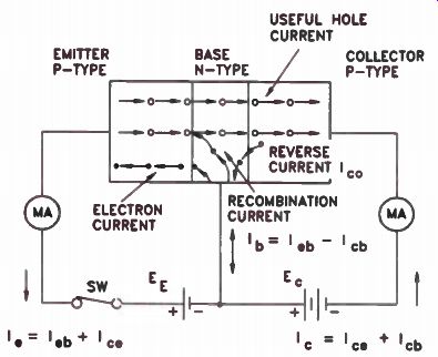
Figure 5. Current flow and carrier movement in a PNP junction transistor.
Some of these holes cross the junction into the n-type base where they pick up an electron and disappear. This is the recombination current.
Most of the holes produced in the emitter cross the emitter-base junction into the base where they are attracted by the negative potential applied to the collector. These holes cross the base, the base-collector junction, and flow to the collector terminal connected to the negative terminal of the battery Here the holes pick up electrons and disappear.
There is another current crossing the base collector junction due to minority carriers found in the depletion layer. Electrons formed on the collector side of the junction cross over and are attracted by the positive terminal of the battery, which connects to the base-collector junction.
Similarly, holes formed on the base side of the depletion layer are attracted by the negative terminal of the battery connected to the collector.
All in all, there are four currents flowing in the PNP transistor, just as in the NPN transistor. The largest of these currents is due to the movement of holes from the emitter through the base, into the collector, to the negative terminal of the battery connected to the collector. In addition to this current, there are three small currents flowing. One is the current created by the electron movement from the negative terminal of the emitter-base battery into the base, across the base, across the junction, and through the emitter to the positive terminal of the battery.
Another is the recombination current due to the holes combining with electrons in the base. And the last one is the reverse current due to the hole-electron pairs being formed in the depletion layer of the base-collector junction. Directions of movement of holes and electrons are shown in Fig.5.
In the PNP transistor, the recombination current is kept as low as possible because it serves no useful purpose, just like the NPN transistor. In the PNP transistor, the recombination current is kept to a minimum by adding more acceptor atoms to the emitter than donor atoms to the base. This makes more free holes in the emitter than there are free electrons in the base, so the recombination current will be quite small. In a good PNP transistor, over 95% of the holes that cross the emitter-base junction flow to the collector.
Note the similarities and differences between the PNP and NPN transistors. In both transistors, useful current comes from majority carriers in the emitter of the transistor. In the NPN transistor, electrons flow from the negative terminal of the battery, through the emitter, across the emitter-base junction and the base, across the base-collector junction, and through the collector to the positive terminal of the battery.
In the PNP transistor, electrons flow from the negative battery terminal to the collector, where they fill holes arriving at the collector terminal.
The positive terminal of the emitter-base battery attracts electrons from the emitter, and these electrons flow through the battery over to the positive terminal of the base-collector battery.
Meanwhile, the holes produced by the emitter terminal of the battery move across the emitter, the emitter-base junction, the base, the base collector junction, and the collector to the terminal connected to the negative terminal of the battery. There they are filled by electrons.
Notice that in both types of transistors, current flows by majority carriers; and that in both cases the majority carriers move from the terminal of the battery connected to the emitter, across the emitter, across the emitter-base junction, across the base, across the base-collector junction, and through the collector to the terminal of the battery connected to the collector. In the external circuit of the NPN transistor (the circuit made up of the batteries), the electrons are flowing in the same direction as the majority carriers in the transistor. In the PNP transistor, since the majority carriers in the transistor are holes, the electrons in the external circuits are flowing in a direction opposite that of the majority carriers.
We have covered a great deal in this section on transistors, and it would be a good idea to review this section again. The important thing to remember is that the useful current through a transistor is by majority carriers. In the NPN transistor the majority carriers are electrons and in the PNP transistor the majority carriers are holes.
You should also notice the polarity of the batteries used to forward bias the emitter-base junction and reverse bias the base-collector junction.
To forward bias the emitter-base junction to an NPN transistor, you connect the negative terminal of the battery to the emitter and the positive terminal to the base. To forward bias a PNP transistor, connect the positive terminal of the battery to the emitter and the negative terminal of the battery to the base. To reverse bias the base-collector junction of an NPN transistor, you connect the negative terminal of the battery to the base and the positive terminal to the collector. To reverse bias the base-collector junction of a PNP transistor, you connect the positive terminal of the battery to the base and the negative terminal of the battery to the collector.
Alloy-Junction Transistors
The first transistors were germanium grown junction transistors. This transistor is made from a small rectangular bar cut from a germanium crystal that has been grown. Suitable impurities are added so that the NPN regions shown in Fig.6 are formed. The base of the transistor, which is kept as thin as possible, is located midway between the two ends. Suitable contacts are welded to the emitter, base, and collector regions.
The disadvantage of this type of transistor is that it is not particularly well-suited for operation at high frequencies. In addition, it is temperature-sensitive and can become quite unstable at high temperatures.
Modern transistors are silicon alloy-junction transistors. There are a number of different types of alloy-junction transistors. In this section of the lesson we are going to discuss these transistors briefly. You do not have to remember the name of each type; they are all junction transistors and work in basically the same way.
A PNP alloy-junction transistor is made by taking a small rectangular piece of n-type semi conductor material and fusing small dots of indium into it on opposite sides, as shown in Fig.7.
This results in p-type material being formed at the points where the dots are fused into the wafer, making a PNP transistor.
An NPN transistor can be made by taking a piece of p-type semiconductor material and fusing a lead antimony alloy into the two opposite sides. It is possible to get more uniform penetration of the lead antimony alloy into the semiconductor material in this type of transistor, and thus better junction spacing. This cuts down on the width of the material between the emitter and the collector and gives improved high frequency performance.
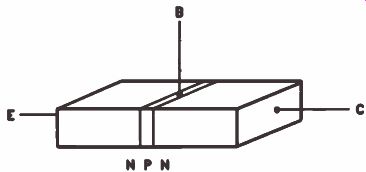
Figure 6. A grown-junction transistor.
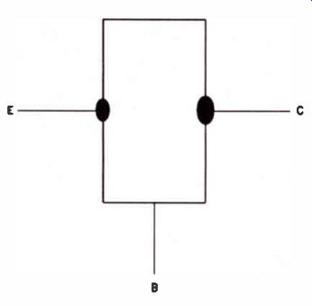
Figure 7. An alloy-junction transistor.
This type of transistor operates better at higher frequencies than the grown-type junction transistor. It has a higher potential for amplification, and remains stable as the temperature increases.
The surface-barrier transistor is an alloy junction transistor in which pits are etched into the silicon, as shown in Fig.8, before adding the impurities that form the emitter and collector.
Surface-barrier transistors perform well at high frequencies.
Notice that in both Fig.7 and Fig.8 the collector is larger than the emitter. In Fig.8(B) we have shown the way in which the majority carriers spread out as they cross the base, traveling from the emitter to the collector.
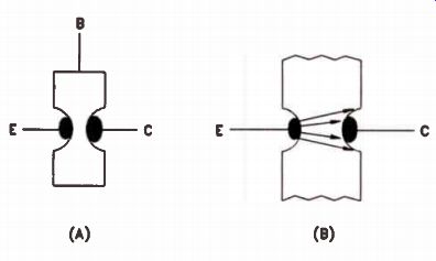
Figure 8. (A) Sketch of a surface-barrier transistor. (B) Hole movement
across the base.
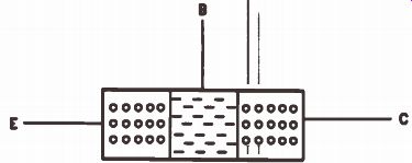
Figure 9. Diagram showing how a large number of donor impurities increases
the electron concentration in the base.
Diffusion Transistors. Diffusion is the pas sage of one material through another. Although a material might look and feel solid, there is a lot of space between its atoms. If you filled a sealed glass jar with hydrogen and allowed it to sit for several days, you would find that the hydrogen had escaped and that the glass was filled with air. Hydrogen atoms are very small and very active, and simply diffuse through the glass. This technique is used in the manufacture of the drift transistor, the mesa transistor, and the planar transistor, all of which are classified as diffusion transistors.
In the drift type of PNP transistor shown in Fig.9, the emitter-base and the collector-base junctions are formed by the alloy technique, but the base region is made by the diffusion process in which the impurities in the base region are varied. In a typical transistor of this type, the concentration of the donor impurities added to the base is controlled so that concentration is highest at the region of the emitter-base junction, then drops off quickly, and finally reaches a constant value which it maintains over to the base-collector junction.
The PNP mesa transistor starts with a piece of p-type material, to which donor impurities are added to form the base region, as shown in Fig.10. After the base is formed, acceptor impurities are added to form the emitter and emitter base junction.
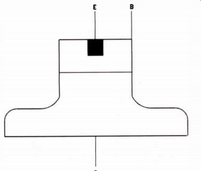
Figure 10. A mesa transistor.
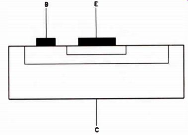
Figure 11. A diffused planar-type transistor.
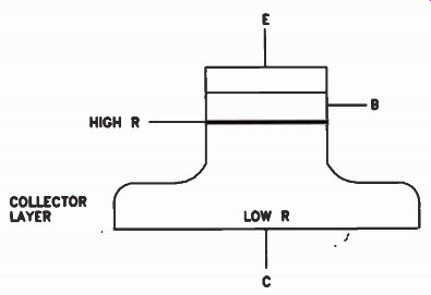
Figure 12. A double-diffused epitaxial transistor.
The advantages of the mesa transistor are good high-frequency response and very consistent performance. It is possible to control the manufacturing techniques quite closely so that the characteristics of mesa transistors of the same type are quite similar. This is not necessarily true of other transistors; their characteristics often vary over a wide range.
An NPN planar transistor is formed from n type silicon. Acceptor impurities are diffused into a region to form the base, as shown in Fig.11.
The donor impurities are then diffused into a small region in the center of the base to form the emitter. Notice that because all junctions are brought back to the same plane, this type of transistor is called planar. Planar transistors usually have a very low reverse current.
Epitaxial Transistors. One disadvantage of the diffusion-type transistor is the relatively high resistance of the collector. This limits its usefulness at high frequencies. If we reduce the resistance of the collector, we introduce the possibility of a collector-base or a collector-emitter short, which destroys the transistor. Both these problems can be overcome with an epitaxial transistor, shown in Fig.12. In this type of transistor, the collector region immediately adjacent to the base-collector junction is doped to have a high resistance. The remainder of the collector is doped to have a low resistance. This technique improves the high-frequency performance of the transistor and at the same time reduces the possibility of a collector short.
Review
Remember that in an NPN transistor the majority carriers are electrons. They cross the emitter to the emitter-base junction. A few electrons leave the transistor at the base, but most cross the base-collector junction and flow through the collector to the positive voltage source. In a good NPN transistor, over 95% of the electrons crossing the emitter-base junction eventually reach the collector.
In a PNP transistor the majority carriers are holes. They are produced in the emitter because electrons are pulled out of the emitter by the positive terminal of the voltage source connected to the emitter. The holes cross the emitter and the emitter-base junction and enter the base. A few of the holes travel over to the base terminal where they are filled by electrons, but most of the holes cross the base, the base-collector junction, and the collector. Here they are filled by electrons from the external voltage source. In a good PNP transistor, over 95% of the holes produced in the emitter cross the base to the collector.
Self-Test Questions
1 What two materials have been used in the manufacture of transistors?
2 What two types of junction transistors are widely used?
3 What type of bias is used across the emitter base junction of a transistor?
4 What type of bias is used across the collector base junction of a transistor?
5 Draw a diagram of a PNP transistor and show how the batteries are connected to place the correct bias across the two junctions.
6 Draw a diagram of an NPN transistor and show how the batteries are connected to place the correct bias across the two junctions.
7 What are the useful current carriers in a PNP transistor? 8 What are the useful current carriers in an NPN transistor?
----------------------
FIELD-EFFECT TRANSISTORS
So far, you have studied NPN and PNP transistors. These transistors are called bipolar devices because their operation depends on the interaction of holes and electrons. The field-effect transistor is a unipolar device, whose operation depends on either holes or electrons, but not both.
Field-effect transistors can be divided into two types: the junction-gate field-effect transistor and the insulated-gate field-effect transistor.
Let's look at the junction-gate field-effect transistor first.
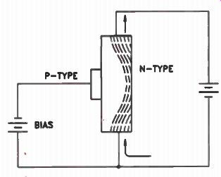
Figure 13. Drawing showing the basic operation of a field-effect transistor.
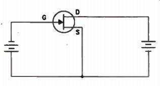
Figure 14. Schematic representation of the n-channel FET circuit shown
in Fig.13.
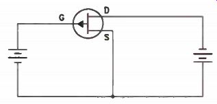
Figure 15. Schematic of a circuit using a p-channel JFET.
Junction-Gate Field-Effect Transistors
One type of junction-gate field-effect transistor is made from a piece of n-type material, as shown in Fig.13. If the negative terminal of a battery is connected to one end of the material and the positive terminal to the other end, electrons flow through the material from one end to the other. If we attach a piece of p-type material to one side so that a pn junction is formed, and place a negative voltage on the p-type material, as shown in Fig.13, there can be no current flow across the junction, because the junction is reverse-biased.
However, the negative voltage applied to the p-type material creates a field that extends into the n-type material. This field blocks the flow of electrons through the n-type material, forcing them to one side, as shown in Fig.13. We call the n-type material a channel. The p-type material is called the gate. The effect of the gate is to narrow the channel and increase its effective resistance. A very high negative voltage applied to the gate can completely block the flow of electrons through the n-type channel. This type of transistor is called an n-channel junction field effect transistor, or n-channel JFET. Figure 14 shows the schematic diagram of the circuit in Fig.13. The end at which the electrons enter the channel is called the source, S. The other end, where electrons exit the channel, is called the drain, D. Notice the direction in which the arrow is drawn; this indicates a p-type gate, which means that the transistor is an n-channel JFET. A p-channel JFET is created by using p-type material as the channel and n-type material as the gate. Figure 15, on the next page, is the schematic of a circuit similar to Fig.14 using a p-channel JFET. Notice that the direction in which the arrow is pointing is reversed to indicate an n-type gate and a p-channel JFET. In the p-channel JFET, the battery connections to source and drain are reversed. Electrons in the p-channel material move toward the positive terminal of the battery, leaving holes behind them. At the circuit connection to the drain, the holes are filled by electrons from the negative terminal of the battery Thus, there are holes moving through the channel from the source to the drain, but electrons are flowing in the external circuit in the opposite direction.
Notice that the battery connected between the gate and the source is also reversed. This battery is called the bias battery. The holes traveling through the channel are repelled by the positive voltage on the gate. Increasing this positive voltage can reduce, or cut off the flow of holes through the channel completely.
As you can see, in the n-channel JFET the number of electrons flowing through the channel depends upon the amplitude of the bias voltage.
Similarly, in the p-channel JFET, the number of holes traveling through the channel depends upon the bias voltage. When this voltage varies, the carriers traveling through the channel vary.
This characteristic of a JFET allows a relatively small signal voltage on the gate to control a much larger, or amplified, voltage in the output circuit.
We will discuss amplification in a later lesson.
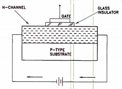
Figure 16. Current flow through an n-channel IGFET with no bias applied.
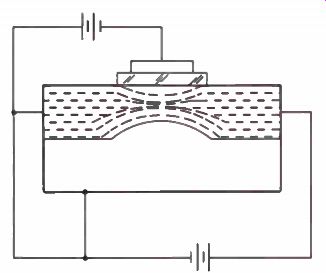
Figure 17. Current flow through an n-channel IGFET with bias applied.
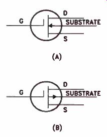
Figure 18. Insulated-gate, field-effect transistors. (A) Schematic symbol
for an n-channel unit, and (B) the symbol for a p-channel unit.
Insulated-Gate Field-Effect Transistors
In addition to the junction-gate field-effect transistor, there is an insulated-gate field-effect transistor; or IGFET. In the IGFET, the gate is completely insulated from the channel by a thin insulating material. For example, a very thin piece of glass or mica might be placed between the conducting channel and the gate. Thus, there is no actual junction formed between the semi conductor materials in the channel and gate.
To make an n-channel IGFET, we start with a lightly doped p-type material called the substrate. Donor atoms are diffused into the top of the substrate to form an n-channel as shown in Fig.16. A glass insulator placed on the side of the channel insulates the gate. When a battery is connected across the n-channel as shown in Fig.17, electrons leave the battery and flow to the source, through the channel, to the drain, and back to the positive terminal of the battery.
When a negative voltage is placed between the gate and the source as shown in Fig.17, the channel is effectively narrowed so that the resistance of the channel increases according to the magnitude of the gate voltage.
Instead of using an n-type material for the channel and a p-type material for the gate in an IGFET, a thin piece of metal that has been oxidized on one side is used for both the gate and the insulator. Metal oxides can be used as insulators because they do not conduct electricity.
The advantage of this arrangement is that the oxide of the metal can be made very thin, putting the metal gate much closer to the channel. This type of device is called a metal oxide, semiconductor field-effect transistor. Sometimes you'll see this abbreviated as MOS field-effect transistor, but more often you see it abbreviated MOS FET (pronounced Mosfet). Both n-channel and p-channel MOSFETs are manufactured. The schematic symbols used to represent the two types are shown in Fig.18.
Figure 18(A) shows the symbol for an n-channel type, and Fig.18(B) shows the symbol for a p channel type. They work essentially the same way as JFETs, except that there is no current flow at all from the channel to the gate or from the gate to the channel. In the JFET, there may be a very small leakage current across the junction. In the MOSFET, however, there is no current flow between the gate and the channel.
Both the JFET and the IGFET (MOSFET) discussed so far use a reverse bias between the junction and the channel. This reverse bias reduces the number of carriers passing through the channel. If the bias is made high enough, it prevents the flow of carriers through the channel, or is said to deplete the carriers in the channel. Thus, these FETs are known as depletion types. There is another type of FET called an enhancement type. Let's see how it works.
All enhancement-type FETs are insulated gate FETs. In the enhancement type, there is no channel. The channel is formed between the source and drain when we place a forward bias between the gate and the substrate. You cannot have an enhancement type JFET because the forward bias would cause a high current to flow through the gate.
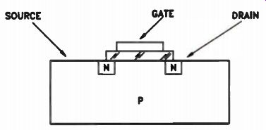
Figure 19. Sketch of an enhancement-type IGFET.
A sketch of an n-channel enhancement type of IGFET is shown in Fig.19, on the next page. We start with a p-type substrate and diffuse two n-type regions into it, one for the source and one for the drain. Notice that there is a space between them and no direct channel from the source to the drain. The gate is placed so that it is opposite part of both the source and the drain.
When the negative terminal of a battery is connected to the source and the positive terminal to the drain, there is no current flow because there is no channel. If we add a second battery with its negative terminal connected to the source and its positive terminal connected to the gate, the positive voltage applied to the gate forces holes out of the p-type region between the source and the drain. At the same time, the negative voltage applied to the source forces electrons out of the source into the region between the source and the drain where they are attracted by the positive voltage applied to the drain. This creates a channel.
The higher the positive voltage applied between the source and the gate, the more holes are forced out of the p-type region between the source and the gate, and the more electrons are forced from the source into the channel and across the channel to the drain. Thus, increasing the voltage between the source and gate has the effect of reducing the resistance between the source and drain by creating a larger channel.
Figure 20 shows the schematic symbols for the enhancement-type IGFETs. The one shown in Fig.20(A) is for an n-channel and the one shown in Fig.20(B) for a p-channel. Compare these symbols with those shown in Fig.18. Notice that in Fig.18 there is a direct line between the source and drain in each case. This indicates that the channel exists, or in other words, that these are depletion-type IGFETs. In Fig.20, a direct line between the source and drain is not shown Because the channel does not exist unless the correct voltage is applied to the gate. Thus, these are enhancement-type IGFETs.
In this discussion, we have referred to both the depletion-type and enhancement-type insulated gate transistors as IGFETs since they are both insulated-gate field-effect transistors. However, you'll see them referred to as MOSFETs in al most every case because the gate of most IGFETs is a piece of metal and the insulation is an oxide formed on the metal. Don't let this confuse you; a MOSFET is a kind of IGFET. However, the term IGFET covers all insulated-gate field-effect transistors regardless of the materials used to insulate the gate.
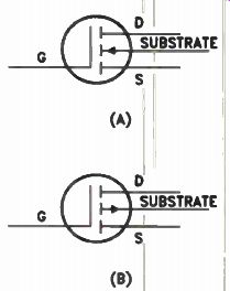
Figure 20. The schematic symbol for (A) an n-channel enhancement-type
IGFET and (B) a p-channel unit.
Review
Field-effect transistors are widely used in electronic equipment. There are two basic types, the junction-gate field-effect transistor (JFET) and the insulated-gate field-effect transistor (IGFET). Remember that in most IGFETs the gate is a piece of metal oxidized on one side. The oxide is the insulator between the gate and the channel. This type of field-effect transistor is usually called a MOSFET. Also, remember that field-effect transistors can be made in both n-channel types and p-channel types. In a depletion-type IGFET, a channel is present and the voltage applied to the gate reduces the width, and hence, increases the resistance, of the channel. In the depletion-type field-effect transistor, the gate is always reverse biased so there is no current flow between the gate and the channel except a small leakage current that might exist.
An IGFET can be either depletion-type or enhancement-type. In the enhancement-type IGFET, the channel between the source and drain does not exist until a voltage is applied to the gate.
Self-Test Questions
9 What is the difference between a junction gate field-effect transistor and an insulated gate field-effect transistor?
10 What is a depletion-type field-effect transistor?
11 What is an enhancement-type field-effect transistor?
12 Is a MOSFET a junction-gate field-effect transistor or an insulated-gate field-effect transistor?
ANSWERS TO SELF-TEST QUESTIONS
1. Germanium and silicon.
2. NPN and PNP.
3. Forward bias is used across the emitter-base junction. To forward bias the emitter-base junction in an NPN transistor, the base is made positive with respect to the emitter.
To forward bias the emitter-base junction in a PNP transistor, the base is made negative with respect to the emitter.
4. Reverse bias is used across the collector-base junction. To reverse bias the collector-base junction in an NPN transistor, the collector is made positive with respect to base. To reverse bias the collector-base junction in a PNP transistor, the collector is made negative with respect to base.
5. See Fig.5.
6. See Fig.3.
7. The useful current carriers in a PNP transistor are holes.
8. The useful current carriers in an NPN transistor are electrons.
9. In a junction-gate field-effect transistor, the gate is in contact with the channel. In the insulated-gate field-effect transistor the gate is insulated from the channel.
10. A depletion-type FET is a unit in which the channel is present between the source and the drain.
11. An enhancement-type FET is a unit in which there is no channel between the source and drain until the operating bias is applied to the gate.
12 A MOSFET is an insulated-gate field-effect transistor where the gate is made of a metal and the insulator is an oxide of the metal.
Lesson Summary Some of the important facts you should remember from this lesson are:
• Junction transistors are three-element semiconductor devices.
• The two basic types of junction transistors are NPN and PNP.
• Forward bias allows conduction of electrons through a transistor, from emitter to collector.
• Reverse bias prevents current flow from emitter to collector of a transistor.
• Field effect transistors utilize field energy and polarity to establish or block a "channel- through a semiconductor material.
LESSON QUESTIONS
This is Lesson Number 2226.
Make sure you print your name, student number, and lesson number in the space provided on the Lesson Answer Form. Be sure to fill in the circles beneath your student number and lesson number.
Reminder: A properly completed Lesson Answer Form allows us to evaluate your answers and speed the results and additional study material to you as soon as possible. Do not hold your Lesson Answer Forms to send several at one time. You may run out of study material if you do not send your answers for evaluation promptly.
1. In a correctly biased NPN transistor, the base is:
a. Negative with respect to the emitter and negative with respect to the collector.
b. Negative with respect to the emitter and positive with respect to the collector.
c. Positive with respect to the emitter and negative with respect to the collector.
d. Positive with respect to the emitter and positive with respect to the collector.
2. In a correctly biased PNP transistor the base is:
a. Negative with respect to the emitter and negative with respect to the collector.
b. Negative with respect to the emitter and positive with respect to the collector.
c. Positive with respect to the emitter and negative with respect to the collector.
d. Positive with respect to the emitter and positive with respect to the collector.
3. Which of the following transistors is a unipolar device?
a. Alloy-junction transistor.
b. Diffusion transistor.
c. Epitaxial transistor.
d. Junction-gate field-effect transistor.
4. Which of the following transistors is a bipolar device?
a. A JFET.
b. An IGFET.
c. An epitaxial transistor.
5. What is a MOSFET?
a. A JFET.
b. An IGFET.
c. An NPN transistor.
d. A PNP transistor.
6. In an NPN transistor, what happens to an electron that crosses the emitter and the base and moves into the collector?
a. It remains in the collector.
b. It fills a hole in an acceptor atom.
c. It returns to the base where it fills a hole.
d. It is attracted to the positive terminal of the battery
7. In a PNP transistor, what happens to a hole that crosses the emitter and the base and moves into the collector?
a. It remains in the collector.
b. It is filled by an electron from a donor atom.
c. It returns to the base to be filled by a free electron.
d. It is filled by an electron from the battery
8. In a PNP transistor, electrons crossing from the base to the emitter:
a. Serve no useful purpose.
b. Increase the movement of holes through the transistor.
c. Make it easier for holes to cross the base.
d. Prevent electrons from crossing the base collector junction.
9. Which of the following is the schematic symbol for an n-channel enhancement type MOSFET?
10. Which of the schematic symbols in the preceding question is the schematic symbol for a p-channel depletion-type MOSFET?
-----------
NRI Schools
DIG A LITTLE DEEPER
A poor farmer struggled for years to gain a living out of the rocky soil, then finally gave up in despair and sought fortune elsewhere. Years later, more wealth was being dug out of this rocky old farm every day than the farmer had ever dreamed existed. The farm had become a gold mine.
Many of us struggle along just like that poor farmer, never dreaming that success could be ours if we dug a little deeper right where we were. Millions of people are just barely getting along today, when they have the ability to do much better things, simply because they lack confidence in themselves. They are victims of mental defeat; they don't believe they can do anything better.
If you lack self-confidence and persistence--if you lack a sense of mastery, a consciousness of power, and a victorious mental attitude, begin now to cultivate self-confidence. How? Make your decisions with confidence and stick to them. Dig into your work a little harder, keep going a little longer, and soon you'll have the confidence that carries you speedily to success.
---------------------------