AMAZON multi-meters discounts AMAZON oscilloscope discounts
An amplifier is a circuit designed to take a weak signal at its input, and produce an amplified copy of the original signal at its output. Often, amplifiers are classified according to the frequencies they are designed to handle. In the first part of this lesson, we will study low frequency amplifiers. Later in this lesson, you will study high or radio frequency amplifiers. Both types of amplifiers are important, because you will find either or both of them in practically every type of electronic equipment.
Amplifiers can also be classified as either voltage amplifiers or power amplifiers. A voltage amplifier is one that is designed to amplify a weak signal voltage, and make it stronger. A number of voltage amplifiers may be used in cascade to take a very weak signal voltage, and amplify it to a usable value. Power amplifiers are used to produce power to drive some external device. For example, every radio receiver has a power amplifier in the output. It takes the audio signal voltage that has been detected and amplified by preceding stages, and produces the power necessary to drive the loudspeaker to produce sound.
The ability of transistors to amplify signals is essentially what makes many of our modern electronic devices possible. Therefore, if you understand how these amplifiers work, and how they are put together to perform specific tasks, you will be able to analyze the operation of many different types of electronic equipment. Since amplifiers are so important, it is worthwhile to spend as much time as necessary on this lesson to be sure you have a complete understanding of them.
TYPES OF AMPLIFIERS
When we speak of low-frequency amplifiers, we are generally concerned with amplifiers that are designed to amplify low frequency signals.
No sharp dividing lines exist at the low frequency or high-frequency end of the range over which the amplifier is supposed to work.
Originally, a low-frequency amplifier was an amplifier that operated in the audio range, within the limits of our hearing. Of course, these amplifiers will amplify signals beyond these frequency limits, but not as well. The basic low-frequency amplifier can be modified so that it can amplify signals over a much broader range than the audio range. In fact, video amplifiers, which amplify picture signals having frequencies up to several megahertz, are simply modified low-frequency amplifiers.
Radio frequency amplifiers can be designed to amplify a specific frequency signal, or to amplify signals over a specific frequency range.
There are radio frequency amplifiers designed for very low frequencies, as low as 18 to 20 kHz.
Other radio frequency amplifiers are designed to amplify very high-frequency signals over 1000 MHz. While they all do the same thing, the circuitry may be quite different because of the frequency of the signal being handled.
When we study low-frequency amplifiers in this lesson, we will study both voltage and power amplifiers. However, we will limit our study of radio frequency amplifiers to voltage amplifiers.
We'll start our study of low-frequency voltage amplifiers with the most widely used amplifier, the resistance-capacitance coupled voltage amplifier.
Resistance-Capacitance Coupled Voltage Amplifiers
Resistance-capacitance coupling, most often called RC coupling or resistance coupling, is so named because resistors and capacitors are used to couple the signal from one stage to another.
This type of coupling is widely used between voltage amplifiers and between voltage amplifiers and Class A power amplifiers in audio work.
You will learn about Class A power amplifiers later in this lesson. While the low-frequency amplifiers we will be discussing are primarily designed to amplify audio or sound signals, remember that these amplifiers can be used to amplify any low-frequency signal.
A Two-Stage NPN Transistor Amplifier
In Fig.1, we've shown a typical two-stage transistor RC coupled amplifier using NPN transistors. We are going to explain the operation of this amplifier in considerable detail because it is very important that you understand exactly how it works. After you have studied this amplifier, you will study another two-stage amplifier using PNP transistors.
The input signal to be amplified is fed into the input terminal in Fig.1 and coupled through C1 to the base of Q1. C2 holds the emitter at ground potential insofar as the signal is concerned, because it has a high capacitance and therefore a very low reactance. The signal is applied directly between the base and the emitter of the transistor. It is in series with the forward bias across the emitter-base junction.
The applied signal, which is an AC signal having a frequency in the audio range, causes the emitter-base current to vary, which in turn causes the collector current to vary. The varying collector current causes a varying voltage drop across R4, so that the effective voltage between the collector of the transistor and ground is varying.
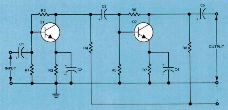
Figure 1. A two-stage RC coupled amplifier using NPN transistors.
If the input signal drives the base in a positive direction, the collector current will increase.
This will cause the voltage drop across R4 to increase, so the voltage between the collector of the transistor and ground decreases. On the other hand, if the input signal swings the base in a negative direction, this will cause the collector current to decrease, because it reduces the forward bias across the emitter-base junction. When the collector current decreases, the voltage drop across R4 will decrease, so the voltage between the collector of the transistor and ground will increase. In other words, when the input signal swings positive, the signal between the collector of the transistor and ground swings negative. When the input signal swings negative, the voltage between the collector of the transistor and ground swings positive. Thus, we have a 180° phase reversal, which happens in the common-emitter amplifier circuit.
The varying input signal applied to the input of Q1 results in an amplified varying signal appearing between the collector of Q1 and ground. This is coupled through C3 to the base of Q2. The way this happens is quite simple.
With no signal applied, there will be a certain current flow through Q1 and a voltage drop across R4, so that the collector of Q1 will be at a certain positive voltage. At the same time, there will be a current flow from ground, which is connected to the negative side of the power supply, through R5, R6, R8, and back to the positive side of the supply that will place the base of Q2 at a slightly positive voltage.
Capacitor C3 will charge to a value equal to the difference between the base voltage of Q2 and the collector voltage of Q1. It will charge with the polarity shown.
When the input signal causes the collector current of Q1 to increase, the voltage drop across R4 increases, and the net voltage between the collector of Q1 and ground decreases. The voltage between the collector of Q1 and the base of Q2 is lower, so C3 must discharge to this lower voltage level. When C3 discharges, electrons flow out of the negative plate through R5 to ground. This will set up a voltage drop across R5, having a polarity that makes the base end negative. The capacitor will have to discharge the same voltage that the collector voltage of Q1 drops. Thus, we have a negative signal at the collector of Q1 appearing at the base of Q2.
When the input signal swings the base of Q1 negative, the collector current decreases, and the voltage drop across R4 decreases. This causes the voltage between the collector of Q1 and ground to increase. C3 must charge to this new value. To charge the capacitor, electrons flow from ground through R5 into the negative plate of C3, out of the positive plate, and through R4 to the plus side of the power supply.
The electrons flowing through R5 to charge C3 to the higher voltage develop a positive voltage at the end of the resistor that is connected to the base of Q2, so that the swing in positive voltage at the collector of Q1 appears at the base of Q2.
The signal appearing between the collector of Q1 and ground is coupled through the RC network, consisting of C3 and R5, to the base of Q2. The emitter of Q2 is held at signal ground potential by C4 so the signal is appearing directly between the base and the emitter of Q2.
The positive-going signal at the input of Q1, which produced a negative-going signal at the collector of Q1, produces a negative-going signal at the base of Q2. This reduces the forward bias across the emitter-base junction so that the current through Q2 goes down. If the collector current of Q2 decreases, the voltage drop across R8 will decrease, so that the voltage between the collector of Q2 and ground will increase. Notice that we have an increasing voltage at the base of Q1, producing an increasing voltage between the collector of Q2 and ground.
When the input signal to the base of Q1 swings in a negative direction, the current through the transistor and R4 decreases. The voltage drop across R4 will decrease, so the voltage between the collector of Q1 and ground swings positive. This will cause the voltage between the base of Q2 and ground to swing positive; the current through Q2, and hence the collector current, will increase.
This will increase the voltage drop across R8 so that the voltage between the collector of Q2 and ground decreases. In other words, we have a negative input signal at the input of Q1 producing a negative-going signal at the output of Q2.
In both cases, the input signal at the input of Q1 is in phase with the output signal at the output of Q2. This is what we might expect. We know that in a common-emitter amplifier, we have a 180° phase shift. So we have a 180° phase shift in Q1 and another 180° phase shift in Q2.
Two 180° phase shifts equal 360°, so that the output signal after going through two amplifier stages will be in phase with the input signal.
The output signal between the collector of Q2 and ground is coupled through C5 to the output terminal.
Notice how we have provided the forward bias across the emitter-base junction. In Q1, we connect a resistor, R2, between the collector of the transistor and the base. We have another resistor R1 between the base and ground. These two resistors form a voltage-divider network and by selecting the correct values, we can bias the base at the value required. Current will flow from ground through R1 and then through R2 and R4 to the positive side of the power supply.
The value of R4 is usually selected so that the voltage between the collector of Q1 and ground will be about half the power supply voltage.
This will permit the voltage on the collector of the transistor to swing a maximum in either positive or negative direction as the input signal changes. Once the value of R4 has been selected, then the values of R1 and R2 are selected to provide the desired positive voltage on the base of the transistor.
It is important to notice that the base voltage is determined by the voltage drop across R1 and the voltage drop across R2. The voltage drop across each resistor is determined by the resistance of the resistor and the current flowing through it. The current flowing through R2 is made up of the current through R1 plus the base current of Q1. If anything causes the current through R2 to change, the voltage drop across it and the bias on the transistor will change.
Some minority carriers, which are holes, will cross the collector-base junction and flow from the collector into the base. These holes will capture some of the electrons flowing from the emitter to the base. Some of these electrons would normally flow out of the base and through R2, and contribute to the voltage drop across R2, which sets the forward bias across the emitter-base junction.
If the transistor begins to heat, the number of holes crossing from the collector to the base will increase. This will result in an increase in the number of electrons flowing into the base that are captured by these holes. This will cause a further reduction in the base current through R2, causing a voltage drop across R2 to decrease. This will cause the voltage on the base of the transistor to rise. In turn, the current flow through the transistor will increase, causing the transistor to heat still further. When this hap pens, the number of holes crossing from the collector to the base will increase further, capturing still more electrons, which will increase the base voltage even further. Eventually this high base voltage will overheat and destroy the transistor. This action is called thermal run away.
Thermal runaway is prevented by the insertion of R3 in the emitter circuit. If the base voltage tends to rise, the current through the transistor will increase and this will increase the voltage drop across R3. Thus, the emitter will become more positive with respect to ground. If the base voltage becomes more positive, so will the emitter voltage, which will prevent or minimize any increase in forward bias across the emitter-base junction. Thus, the sole purpose of R3 in the circuit is temperature stabilization. R7 in the emitter circuit of Q2 is used for the same purpose.
Let's consider another effect caused by the way we provide this forward bias. When a signal is applied to the input and drives the emitter-base junction in the positive direction so that the collector current increases, the voltage drop across R4 increases so that the collector voltage swings in the negative direction. Thus, the voltage between the collector of the transistor and ground decreases. We are using this voltage to provide the forward bias across the emitter-base junction of the transistors. Therefore, the forward bias will decrease.
The positive-going signal has the effect of in creasing the forward bias on the transistor. The drop in output voltage has the effect of reducing the forward bias on the transistor. This is called degenerative, or negative, feedback. It reduces the effect of the input signal, which in turn reduces the strength of the output signal.
You might at first think this is a disadvantage, but it does have the advantage of increasing the frequency response of the amplifier. The frequency response of the amplifier is its ability to amplify equally all the different frequencies fed to it.
You could see why this is so if you consider what happens if the amplifier has a tendency to amplify some frequency or frequencies more than others. They will appear as a stronger signal in the output of the stage, meaning that the feedback would increase. This will reduce the gain of the stage more than it will in the case of frequencies that receive less amplification. Therefore, the degenerative feedback tends to equalize the gain of the stage over a wide range of frequencies.
When amplifiers are connected one stage after another as they are in Fig.!, we say they are connected in cascade. The total gain of the two amplifiers will be equal to the product of the gain of each stage. If each stage in the example shown in Fig.1 has a gain of 10, the total gain will be 100. Suppose we feed a signal of 10 millivolts into the first stage having a gain of 10. At the output, the signal should have an amplitude of 10 millivolts times 10 equals 100 millivolts. Now, we feed the 100 millivolts into the second stage, where it is again amplified by a factor of 10. We then have 100 millivolts times 10 equals 1000 millivolts or 1 volt.
A Two-Stage PNP Transistor Amplifier
In Fig.2, we've shown a typical two-stage RC coupled amplifier using PNP transistors. The operation of this amplifier is basically the same as the one shown in Fig.1, except that the power supply connections are reversed and the carriers through the transistors will be holes instead of electrons. Notice that we have obtained the forward bias for the emitter-base junction for each transistor in the same way as we did for the NPN transistors in Fig.1. Also, notice in Fig.2 that resistors R3 and R7 in the emitter circuit of each transistor, are used to prevent thermal runaway.
Even though the operation of this two-stage amplifier is basically the same as the one shown in Fig.1, we are going to explain its operation in considerable detail. Read over the explanation carefully in order to note the differences between these two amplifiers.
First, let's consider what is happening in Q1 under zero signal conditions. Essentially the same thing is also happening in Q2. Notice that the emitter of Q1 connects through R3 to the positive side of the power supply. Electrons will be attracted from the emitter through R3 to the positive side of the power supply. The electrons leaving the emitter will produce holes that will cross the emitter-base junction if the base is negative with respect to the emitter.
Notice that the negative side of the power supply connects through R4 to the collector of Q1. Electrons can flow from the negative side of the power supply through R4 to the collector, where they will fill holes arriving at the collector. Some electrons flowing through R4 will flow through R2 and R1 to the positive side of the supply. The voltage drop across R1 will make the base negative with respect to ground.
By selecting the values of R1 and R2 correctly, the base can be made negative with respect to the emitter so we have the correct forward bias across the emitter-base junction.
It is important to notice that the current flow through R2 is made up of the current flow through R1, plus some electrons that will flow into the, base and will fill holes crossing the emitter-base junction. In the PNP transistor, the electrons are the minority carriers and some electrons will cross from the collector to the base and fill some of the holes that would normally be filled by electrons flowing through R2. We have the same condition where thermal runaway cart be produced in the PNP transistor that we had in the NPN transistor. If the transistor current begins to increase because of thermal runaway, the current through R3 will increase. This will swing the emitter in a negative direction, which will reduce the change in potential between the emitter and base, and reduce any change in the forward bias due to the transistor heating.
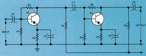
Figure 2. A two-stage RC coupled amplifier using PNP transistors.
When the input signal fed to Q1 swings in a positive direction, it will reduce the forward bias across the emitter-base junction. This will cause the number of holes flowing through the transistor to decrease. When this happens, the current through R4 decreases so the voltage drop across it decreases. This will cause the voltage between the collector of Q1 and ground to swing in a negative direction.
When the input signal swings in a negative direction, it will add to the forward bias across the emitter-base junction. The increased for ward bias will cause the number of holes flowing through the transistor to increase, and therefore the number of electrons flowing through R4 to fill the holes arriving at the collector will increase. This will cause the voltage drop across R4 to increase so that the voltage between the collector of Q1 and ground becomes less negative, or swings in a positive direction.
Notice that we have the same situation in Q1 in Fig.2 that we had in Q1 in Fig.1. The positive- going incoming signal causes the voltage between the collector and ground to swing in a negative direction. A negative-going input signal causes the voltage to swing in a positive direction. In both transistors, we have the 180° phase reversal.
The signal developed between the collector of Q1 and ground is coupled to the RC coupling network consisting of C3 and R5 to the base of Q2. Here the signal is amplified and once again we have the 180° phase reversal that we have in any common-emitter amplifier. The signal at the output of Q2 has gone through a 180° phase reversal in Q1 and a second 180° phase reversal in Q2 and is therefore back in phase with the input signal.
The coupling capacitor, C3, couples the signal from the collector of Q1 to the base of Q2 in the same manner as in the preceding amplifier.
To see how it works, let's consider the amplifier first under zero signal conditions.
With no signal applied to the input, there will be a certain number of holes crossing the emitter-base junction and the base, and flowing to the emitter. These holes will be filled by electrons coming from the negative side of the power supply and flowing through R4. Electrons flowing through R4 will result in a voltage drop across it. The collector of Q1 will be negative with respect to ground. The collector voltage will be approximately one half the supply voltage.
Electrons flowing through R8, R6, and R5 will develop a voltage across R5 so that the base of Q2 is negative with respect to ground. However, the collector of Q1 will be much more negative, so the capacitor C3 will charge with the polarity shown.
When a signal fed to the input swings in a positive direction, it will subtract from the forward bias across the emitter-base junction of Q1, so the number of holes reaching the collector will decrease. This means that the number of electrons flowing through R4 will decrease causing the voltage drop across R4 to decrease. The voltage between the collector of Q 1 and ground will swing in a negative direction so that the voltage between the collector and ground increases. Capacitor C3 must charge to this higher voltage. Electrons will flow from the negative terminal of the power supply through R4 and into the negative plate of C3. Electrons will flow out of the positive plate of C3 through R5 to ground. In flowing through R5, the electrons will cause a voltage to be developed across the resistor having a polarity such that the base end of the resistor will be negative. Thus the negative voltage swing at the collector of Q1 appears as the negative voltage swing at the base of Q2.
When the input signal swings in a negative direction, it will add to the forward bias across the emitter-base junction of Q 1 so the number of holes flowing through the transistor to the collector will increase. This means the number of electrons flowing from the negative side of the supply through R4 to the collector to fill these holes will increase. The increase in current through R4 will cause the voltage drop across it to increase. Thus the negative voltage between the collector of Q1 and ground decreases. Now C3 must discharge to this lower value. Electrons will leave the negative terminal of C3 and flow to the collector to fill some of the holes arriving at the collector of Q1. Electrons will flow from ground through R5 and into the positive side of C3. Electrons flowing through R5 will swing the base voltage in a positive direction. Thus we have the voltage between the collector of Q1 and ground becoming less negative, or swinging in a positive direction and a positive-going voltage appearing between the base of Q2 and ground. The base of Q2 will not swing positive, it will simply be less negative.
As in the case of the two-stage amplifier using NPN transistors, the gain of the two-stage amplifier using PNP transistors will be equal to the product of the gain of each stage. For example, if we have a gain of 10 in each stage, the overall gain of the two-stage amplifier will be 100. A Two-Stage FET Amplifier
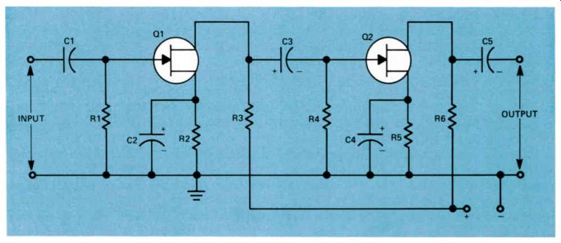
Figure 3. A two-stage RC coupled amplifier using JFETs.
Field-effect transistors are not used as frequently as bipolar transistors in low-frequency voltage amplifiers, but there is no reason why they can't be. A typical two-stage RC coupled amplifier using n-channel FETs is shown in Fig.3.
You will remember that with a junction FET there must be a reverse bias between the gate and the channel to prevent current flow from the channel to the gate. With an n-channel FET, the gate must be negative with respect to the channel. In the circuit, R2 is connected between the source of Q1 and ground, and is used to provide the required reverse bias between the gate and the channel. Current flowing from the negative side of the power supply flows through R2 to the source. In so doing, a voltage is developed across the resistor having a polarity such that the source end is positive with respect to ground. The gate is connected to ground through R1 and since there will be no current flow through R1, there will be no voltage drop across it. The gate will be at DC ground potential. Since the source is positive with respect to ground, it will be positive with respect to the gate. This means that the gate is negative with respect to the source and the channel. R5 is connected between the source of Q2 and ground for the same reason.
Notice that we have a capacitor, C2, connected across R2. This is a large capacity capacitor so it has a very low reactance. Insofar as the signal is concerned, the source of the transistor is connected directly to ground. Therefore any signal fed to the input will be applied directly between the gate and the source.
When the incoming signal swings in a positive direction, it will reduce the reverse bias between the gate and the channel. This will permit the number of electrons flowing through the channel to increase so the voltage drop across R3 increases. Thus the voltage between the drain of the FET and ground decreases.
Under zero signal conditions, C3 will be charged with the polarity shown. When the voltage between the drain of the transistor and ground decreases, the level of the charge on C3 must decrease. Electrons will flow from the negative plate of C3 through R4 to ground, and will develop a voltage having a polarity such that the end connected to the gate is negative.
Thus the negative-going voltage appearing between the drain of Q1 and ground is coupled through C3 to the gate of Q2. The negative voltage on the gate of Q2 will increase the reverse bias between the gate of Q2 and the channel so that current flow through Q2 will decrease. This means that the current through R6 will also decrease so the voltage drop across it will decrease. The voltage between the drain of Q2 and ground will increase. Thus we have a 180° phase reversal on Q1 followed by another 180° phase reversal on Q2 so that the voltage at the output of Q2 is in phase with the voltage at the input.
When the signal at the input swings in the negative direction, it will add to the reverse bias between the channel of Q1 and the gate so the current through Q I will decrease. This will cause the voltage between the drain of Q1 and ground to increase. C3 must charge to this higher voltage. To charge C3 at a higher voltage, electrons will flow from ground through R4 and into the negative plate while electrons will leave the positive plate of C3 and flow through R3 to the positive side of the power supply. The electrons flowing through R4 will develop a voltage so that the gate end is positive. This will reduce the reverse bias between the gate and channel of Q2 so the current flow through the transistor will increase. The increased number of electrons flowing through Q2 will result in a greater voltage drop across R6 so the voltage between the drain of Q2 and ground will decrease. Thus we have a negative-going signal at the input producing a negative-going signal at the output.
As in the preceding examples, the overall gain of the two-stage amplifier is equal to the product of the gain of the individual stages.
Once again, if each stage has a gain of 10, the overall gain of the two-stage amplifier will be 100.
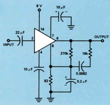
Figure 4. An IC low-frequency amplifier
A Typical IC Amplifier
Integrated circuits are also used as low frequency voltage amplifiers. A typical circuit is shown in Fig.4. This circuit is actually the input circuit of one channel of a stereo tape player.
The input circuit for the other channel is contained in the same IC. The schematic diagram does not indicate what circuit may be used inside the IC. This is the only information you will get on the schematic diagram. If you can find out who manufactured the IC, the chances are that you can find out what circuitry is inside the IC. But as a technician, this information probably won't be of much help to you. You know that the IC is supposed to take a weak signal applied between terminal 2 and ground and produce an amplified signal between terminal 6 and ground.
If you encounter a circuit of this type that fails to work properly, the only thing you can do is check the input signal at terminal 2 and the output signal at terminal 6. If the output signal is much stronger than the input signal, you know that the IC is working. If you do not get an amplified signal at terminal 6, you know there is something wrong with the circuit. With no amplified output signal, you should check the voltage on terminal 14 to be sure that you have 8 volts. If you do, make sure that the external components used in the circuit are good. If they are in good condition, the chances are that the IC is defective, and the only thing you can do is try a replacement.
You might not expect an amplifier such as shown in Fig.4 to have a very high gain because it shows only one block for the IC. However, there is no way of telling what is inside the integrated circuit. Usually there will be a number of stages connected in cascade so that the amplifier normally has considerable gain. Most often amplifiers of this type have a gain of 100 or more.
Operational Amplifiers
Operational amplifiers, which are usually called op amps, are simply a combination of some of the individual amplifier circuits you have already studied. A typical op amp may consist of a differential amplifier directly coupled to an emitter follower, which in turn is coupled to another differential amplifier that is coupled to an emitter follower. In most cases, the device that is used as an operational amplifier has a very high gain, but this gain is controlled by an external feedback network.
Figure 5 is a diagram of a differential amplifier and an emitter follower. You have already studied this circuit, but it is so widely used in op amps we will review it.
Figure 5. A differential amplifier and an emitter-follower combination forming an operational amplifier.
Notice there is no forward bias shown across the emitter-base junction of Q1 and Q2. This is taken care of in the input circuit. You will remember that there are two inputs to this type of amplifier, one marked with a + symbol sign and the other with a - sign. The input marked with the + sign is called the noninverting input.
The reason for this is that the phase of the signal coming out of the emitter follower will be the same as the phase of the input signal. For example, if the signal applied to the input of Q1 swings in a positive direction, this will cause the emitter current through Q1 to increase. This will increase the voltage drop across R1, swinging the emitters of Q1 and Q2 in a positive direction. This will reduce the forward bias across the emitter-base junction of Q2 which in turn will reduce the collector current of Q2. If the collector current goes down, the voltage drop across R2 will go down, so the collector of Q2 will swing in a positive direction. This will increase the forward bias across the emitter base junction of Q3, causing the current through this transistor to increase. This will cause the voltage drop across R3 to increase, and since current flows from ground to the emitter, the emitter will become more positive.
Thus, a positive-going signal applied to the base of Q1 will cause a positive-going signal at the output.
If a positive-going signal is fed to the inverting input, which is marked with a - sign, the positive-going signal will be fed to the base of Q2. This will increase the forward bias across the emitter-base junction of Q2, so that the collector current through the transistor will increase. This will increase the voltage drop across R2 so that the voltage between the collector of Q2 and ground will decrease. This will reduce the forward bias across the emitter base junction of Q3, causing the current to go down. The drop in current will reduce the voltage drop across R3 so that the output signal will swing in a negative direction.
In summary, the signal fed into the non-inverting input, which is marked with a + sign, will cause a signal having the same phase to appear in the output. A signal fed into the inverting input, which is marked with a - sign, will cause a signal 180° out of phase to appear in the output.
The symbol for an op amp is shown in Fig.6.
Input 1, marked with a - sign, is the inverting input and input 2, marked with a + sign, is the noninverting input. The letter A stands for the gain of the op amp. If we apply an input signal to the amplifier, an output signal will be generated. The input signal will be amplified by an amount equal to the gain A of the amplifier. If the input signal is very small, it will appear greatly enlarged at the output because of the high gain.
If the input signal to an op amp is too high, the amplifier output will be clipped. For example, if we apply a 1 volt input signal to an op amp with a gain of 10,000, our output would theoretically be equal to the input multiplied by the gain, or 10,000 volts. This cannot actually happen. The output of any amplifier is limited by the power supply voltages. Most op amps are powered with both positive and negative voltages. A typical op amp, for example, may use power supplies of +12 and -12 volts. For this reason, the output cannot swing any greater than ± 12 volts or no more than 24 volts peak to-peak for a sine wave.
Since the gain of an op amp is so high, it can be used only with very low level signals. Another problem with the op amp is that it is very unstable and its gain may vary considerably from one amplifier to another. One amplifier may have a gain of 10,000, and the next one, which is supposed to be identical, might have a gain of 15,000. For many applications, this is a disadvantage.

Figure 6. Operational amplifier symbol
To overcome this problem we use negative feedback with op amps by feeding some of the output voltage from the amplifier back to the inverting input through a resistor. As you learned earlier, negative feedback reduces the overall gain of an amplifier. At the same time, it stabilizes the amplifier and improves its frequency response.
Figure 7(A) is a diagram of a typical op-amp circuit. Here, the noninverting input to the amplifier is grounded. This eliminates the differential characteristics of the amplifier so we can use it as a single-ended circuit. Negative feedback is provided by resistor R2 connected between the output and the inverting input.
An input resistor, R1, is also connected to the inverting input. The free end of R1 is the input to the circuit. With this circuit, the gain of the op amp is determined entirely by the ratio of R2 to R1 rather than A. If this is difficult to see at first, see Fig.7(B) for an explanation.
Figure 7(B) shows the current and voltages in the op amp circuit. Current flowing through R1 is designated I1, while current flowing through the feedback resistor R2 is designated I2. The current flowing in the input of the op amp is designated 13. 13 is generally the base current of a transistor. The input voltage to this circuit is labeled E1, and the input to the amplifier is shown as E2. The output voltage is Eo.
Since the gain of the amplifier is A, we know that the output voltage is equal to A times the input voltage of the amplifier. We can write this:
Eo = E2 x (-A)
We use a - sign because the input signal is inverted. We can rearrange this formula to find the input voltage of the amplifier:
E2 = E° -A
To continue our explanation, you will re member from earlier lessons that the voltage across any part is equal to the difference in the voltages at the ends with respect to ground. For example, if we measure 10 volts between one end of the resistor and ground, and 4 volts between the other end and ground, the voltage across the resistor is 6 volts.
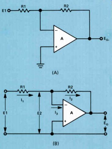
Figure 7. (A) A standard op amp and voltages in the op amp. circuit.
(B) Currents
With this in mind, we can write the formula for the voltage across R1 and R2. The voltage across R1 is equal to E1 - E2. The voltage across R2 is equal to E2 - Eo. Knowing the voltages across the resistance, we can write a simple Ohm's law expression for the current through each resistance. For example, current I1 through resistor R1 is equal to the voltage across it, which is E1 - E2, divided by R1. The current through R2 is equal to the voltage across it, E2 - Eo divided by R2.
In Fig.7(B), the current flowing in the amplifier is 13. If we assume that the op amp is a perfect amplifier and has an infinite impedance, we can conclude that it will not draw current from the input source and 13 = O. In fact, 13 will be so low that this is a valid assumption. The entire input current I1 must flow through R2.
This means that I1 must be equal to 12. Now if: I1 = 12
then, E1 - E2 E2 - E. R1 R2
Earlier we said that the input voltage E2 is equal to the output voltage E. divided by the gain, which is -A. The gain is so high that the input voltage E2 is extremely small. It is so small we can call it zero. If we assume a zero value for E2, we can remove the E2 figure from the formula. Thus,
E1 _ E. R1 - R2
From this we can find that the output voltage is equal to the ratio of the feedback resistance R2 to the input resistance 111 multiplied by the input to the circuit.
E° = - -R2 x El R1
The negative sign indicates inversion.
If you have any difficulty working with these formulas, don't worry. You don't have to go through all the mathematics we have gone through. We show it only for the benefit of those who want to see why the gain of the op amp depends entirely upon the ratio of R2 to R1. All you need to do is remember this ratio.
The important thing to realize is that the op amp is capable of a very high gain, and we can control it so it will be stable by selecting the correct values of the feedback resistor and the input resistor.
While operational amplifiers can be made using discrete components, the operational amplifiers you will encounter will be integrated circuits. Not only is an IC op amp less expensive than one using discrete components, but the characteristics can be controlled better.
There is also less possibility of running into some problem, such as feedback that could cause the amplifier to be very unstable.
Figure 8 is a schematic diagram of one-half of an IC that contains two operational amplifiers.
The other half consists of another operational amplifier that is identical to the one shown. The diodes D1 through D4 are used to help maintain a constant input voltage to the input transistors, Q1 and Q2. D5 and D6 are used to help maintain a constant base voltage to the two constant current sources, Q3 and Q6. Notice that the input to Q1 is the noninverting input, and the input to Q2 is the inverting input. The output from Q1 connects directly to Q4 and the output from Q2 connects directly to Q5. The output from Q5 connects directly to the combi nation of Q7 and Q8, which form an emitter follower. This type of amplifier has considerable gain and could be used as an amplifier in a stereo system, as shown in Fig.4. The amplifier we have shown will be used in one channel, while the other identical amplifier in the IC is used for the other channel.
Even though the gain of the two amplifiers in one IC should be equal since they are all formed at the same time, there might be considerable difference in their gains. However, since the gain is going to be controlled primarily by the ratio of the feedback resistor to the input resistor, by using resistors with a 1% tolerance, you can have two op amps with practically identical gain. For example, with a 1% tolerance one amplifier might have a gain of 100, and the other would have a gain of no less than 99 or more than 101.
The op-amp is a very flexible amplifier. Since its gain can be readily controlled by external resistance, it is a very useful amplifier. In addition, it lends itself to low-cost mass production in ICs so it is widely used in all types of electronic equipment. The three-terminal voltage regulators you studied in a preceding les son use an op amp as the error amplifier.
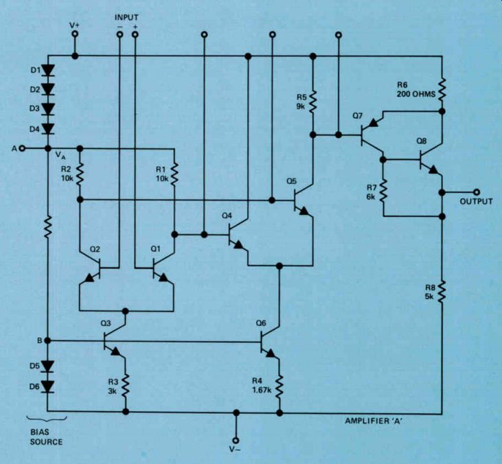
Figure 8. Schematic diagram of one operational amplifier in a dual op
amp IC.
Summary
In the two two-stage amplifiers shown in Figs.1 and 2, there is a 180° phase reversal in each stage so that the signal at the output will be in phase with the signal at the input. In both amplifiers, the amplified signal between the collector of Q1 and ground is coupled through C3 to the base of Q2. In each amplifier the charging and discharging of C3 as the voltage between the collector of Q 1 and ground varies, causes a current to flow through R5 so the varying voltage between the collector of Q1 and ground will be coupled between the base of Q2 and ground. The overall gain of the two stage amplifier is equal to the product of the gain of the two stages.
An operational amplifier is a high-gain amplifier that readily lends itself to IC manufacturing techniques. Op amps have two inputs, an inverting input and a non-inverting input. An op amp has such a high gain that it has a tendency to be somewhat unstable. To prevent this, the gain is controlled by means of feedback from the output to the inverting input. The gain of an op amp will be equal to the ratio of the feedback resistor to the input resistor.
By using a feedback resistor and an input resistor with a tolerance of 1% or less, we can control the gain of an op amp quite precisely.
Self-Test Questions
1 In the amplifier shown in Fig.1, what is the phase relationship between the amplified output voltage and the input voltage?
2 In the circuit shown in Fig.2, if the input signal voltage swings in the positive direction, what will happen to the collector voltage on Q1?
3 In the circuit shown in Fig.3, what is the purpose of R5?
4 In the circuit shown in Fig.4, if the voltage applied to terminal 14 is nor mal, you have an input signal voltage on terminal 2 and all other parts check good, yet there is no output on terminal 6, what should you do?
5 What is the meaning of the + and - signs on the leads going to the base of Q1 and Q2 in Fig.5?
6 What type of circuit is used in Q3 of Fig.5?
7 In Fig.6, what does the letter A in the center of the triangle indicate?
8 What determines the gain of the circuit shown in Fig.7?
9 How many differential amplifiers are there in the circuit shown in Fig.8?
----------------------
LOW-FREQUENCY POWER AMPLIFIERS
After the weak audio signal has been amplified, it is fed to a power amplifier that develops the power necessary to operate the loud-speaker. Power amplifiers can be divided into three classes called Class A, Class B, and Class C. In a Class A power amplifier, the transistor is biased on the midpoint of its characteristic curve. Current flows through the transistor during the entire cycle. We say that current flows for 360°. Class A power amplifiers can be used both as low-frequency power amplifiers and radio frequency power amplifiers.
Class B power amplifiers are biased at cut off. Current flows through a Class B power amplifier only when it is driven into conduction by the incoming signal. Current flows for approximately one half-cycle or for 180°. Class B power amplifiers can be used both as low-frequency power amplifiers and radio frequency power amplifiers. However, when a Class B power amplifier is used as a low frequency power amplifier, two transistors will always be used, one to amplify each half of the cycle. We call this arrangement a push pull amplifier.
A Class C power amplifier is an amplifier that is biased beyond cutoff so that current flows through it for less than one half-cycle. Class C power amplifiers cannot be used as low frequency power amplifiers. Their use is restricted to radio frequency power amplifiers. In a Class C RF power amplifier, current will flow through the transistor for about 120°. Low-frequency power amplifiers using a single transistor are always Class A power amplifiers. They are called single-ended power amplifiers. A low-frequency power amplifier using two transistors may be either a Class A power amplifier or a Class B power amplifier.
In both cases they are called push-pull amplifiers. Let's look at single-ended amplifiers first, then we'll look at push-pull amplifiers.
Single-Ended Power Amplifiers
A single-ended power amplifier is shown in Fig.9. This amplifier is a Class A amplifier. A Class A amplifier is biased at the midpoint of its characteristic curve. This means that the forward bias across the emitter-base junction is adjusted so that the current flowing through the transistor is halfway between zero current and maximum current.
The transistor used in the circuit of Fig.9 is an NPN transistor. Forward bias for the emitter base junction is provided by R1 and R2. Current flowing from ground through R1 will develop a voltage across the resistor having the polarity so that the end connected to the base will be positive. Current flowing through R3 will also develop a voltage across this resistor so that the emitter is positive with respect to ground.
However, the values of R1 and R2 are adjusted so the base is more positive than the emitter.
Thus, the base current will be equal to the current needed to cause the collector current to be about halfway between zero and saturation.
When the incoming signal swings in a positive direction, the base current will increase, causing the collector current to increase. An equal swing in the input signal in a negative direction will cause an equal decrease in base current and hence an equal decrease in collector current. As a result, the average current through the transistor does not change.
The varying collector current flows through the primary winding of T1, which is called an output transformer. The output transformer is a step-down transformer and is used to match the comparatively high output impedance of the transistor to the low impedance of the speaker voice coil. A step-down transformer will produce a step-up in the current so that a relatively high current flows through the secondary winding of the output transformer and through the speaker voice coil. This will cause the speaker voice coil and the speaker cone to vibrate in and out generating sound.
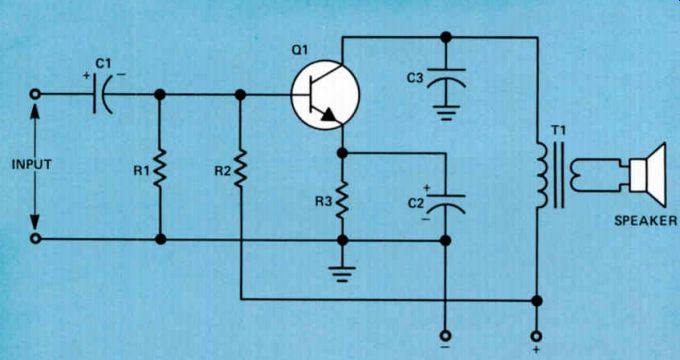
Figure 9. Schematic diagram of single-ended Class A amplifier using an
NPN transistor.
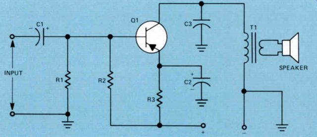
Figure 10. Schematic diagram of single-ended Class A amplifier using
a PNP transistor.
Capacitor C2 is a large capacitor and there fore has a low reactance. As far as the input signal is concerned, the emitter is connected directly to ground. Resistor R3, connected between the emitter of a transistor and ground, is used to prevent thermal runaway.
Capacitor C3, connected between the collector of the transistor and ground, is needed to prevent parasitic oscillations. These are unwanted high-voltage signals that might develop between the collector of the transistor and ground. These signals can have a high enough amplitude to arc through the transistor and destroy it. Capacitors C1 and C2 are relatively large capacity capacitors that offer little or no reactance at the frequencies to be amplified. C3 is a much smaller capacitor that has a high reactance at the frequencies to be amplified, but a low reactance at the frequency of the parasitic oscillations that might occur.
Figure 10 shows a single-ended Class A power amplifier using a PNP transistor. In this circuit the forward bias across the emitter base junction is set by R1 and R2. When the transistor is operating, electrons are pulled from the emitter and flow through R3. The voltage drop across R3 will have a polarity such that the end connected to the emitter is negative (less positive) with respect to its lower end. Current flowing through R1 and R2 will develop a voltage across R2 so that the base end is more negative (even less positive) than the voltage on the emitter. To forward bias a PNP transistor, the base must be negative with respect to the emitter.
The holes flowing through the transistor will reach the collector, where they will be filled by electrons flowing from the negative side of the supply through the primary winding of the output transformer to the collector.
In this circuit a positive increase in the input signal voltage will cause a reduction in the number of holes flowing through the transistor.
An equal 'amplitude negative input voltage swing will cause an equal increase in the number of holes flowing through the transistor.
The varying number of holes reaching the collector due to changes in the input signal will cause the number of electrons flowing through the primary winding of the output transformer to vary. In turn, this will induce a varying current in the secondary which is in series with the speaker voice coil.
Figure 11 is a simplified sketch showing how the loudspeaker is made. The speaker is made with a permanent magnet usually made of a material called alnico. This is an alloy made of aluminum, nickel, and cobalt that produces a very strong magnet.
The speaker movement consists of a voice coil form on which is wound a voice coil. This is simply a coil consisting of a relatively few number of turns. The voice coil form fits into a slot in the permanent magnet. The leads from the voice coil are cemented to this paper speaker cone. Additional flexible leads are connected to them and they are brought out so they can be connected to the secondary winding of the output transformer.
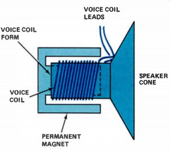
Figure 11. A sketch of a permanent magnet speaker.
The secondary winding of the output transformer is connected in series with the voice coil. The varying current in the secondary of the output transformer causes a varying current to flow through the voice coil. Remember that the output transformer is a step-down transformer, so the varying current will be much greater than the varying current in the primary winding of the transformer. The varying current flowing through the voice coil produces a magnetic field which alternately adds to and opposes the field from the magnet. This causes the voice coil form, and hence the speaker cone, to move in and out at an audio rate. The speaker cone sets the air around it into vibration to produce the sound.
Some speakers are much more elaborate than the simple one shown in Fig.11, but all permanent magnet speakers operate on the basic principle described.
Single-ended, Class A power amplifiers are used in table-model receivers and in most TV receivers. They are used in table-model receivers to keep the cost down. They are used in TV receivers because most people are interested in the quality of the picture rather than the quality of the sound. Since they are less expensive than push-pull amplifiers, you will find them even in expensive color TV receivers. Push-pull amplifiers, however, can produce a higher output, and in some cases, such as in portable receivers, are an advantage because they can be designed to consume less power.
Push-Pull Amplifiers
The push-pull output stage got its name in the early days of radio. In this circuit, two tubes are used so when the current through one increases, the current through the other decreases. The increasing magnetic field, produced in one half of the output transformer, is aided by the decreasing magnetic field produced in the other. Thus, you have the effect of one stage pushing and the other pulling.
A push-pull stage using NPN transistors is shown in Fig.12. In this circuit, forward bias on the transistors is set so they are operating at approximately midway between zero current and saturation. When the input signal causes the base of Q1 to swing in a positive direction and the base of Q2 to swing in a negative direction, the collector current in Q1 will increase while the collector current from Q2 will decrease. This will cause the current through the upper half of the primary winding of T2 to increase and the current through the lower half to decrease. These two changes cause changes in the magnetic field produced by the primary winding of T2, which induces a voltage in the secondary of T2, which in turn causes a high current to flow through it and through the speaker voice coil.
Notice that the resistor R2 in the emitter circuit of Q1 and Q2 is not bypassed. In single ended amplifiers this resistor must be by passed. Otherwise, the varying current through the resistor will produce a varying voltage at the emitter, which will be in phase with the signal voltage applied to the base. This will tend to reduce the net base-to-emitter signal voltage, and hence, the gain of the stage. However in this circuit, as the current through Q1 increases, the current through Q2 decreases an equal amount so that the current through R2 remains constant. Therefore, there is no signal voltage produced across the resistor.
The circuit shown in Fig.12 is a Class A push pull amplifier. Class A push-pull amplifiers are widely used because they produce little distortion. Distortion is any change that occurs in a signal that is amplified. For example, suppose a musical instrument is producing a note as a pure sine wave having a frequency of 300 Hz. If the signal is picked up by a microphone, fed to an amplifier, and the signal shape is changed in the output, we have distortion.
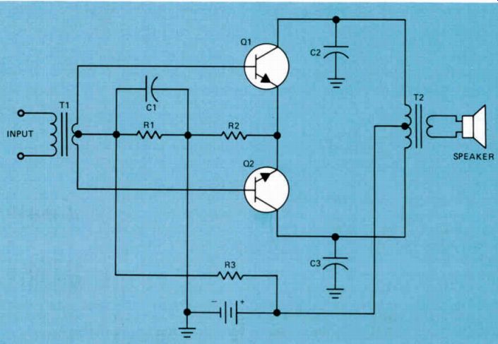
Figure 12. Class A push-pull NPN transistors.
Distortion is also present if any additional signals are added in the amplifier. One of the characteristics of amplifier stages is that they tend to generate harmonics. Harmonics are signals with frequencies that are multiples of the original signal frequency. In other words, when the 300 Hz signal is amplified, a 600 Hz signal may be produced. Since this signal is twice the frequency of the original signal, we call it the second harmonic. In addition, a 900 Hz signal might be produced. This is called the third harmonic because 900 Hz is three times the 300 Hz signal.
An amplifier stage can produce many harmonics but fortunately the second is usually the strongest, the third weaker, the fourth still weaker and so on. One of the characteristics of push-pull amplifiers is that they cancel any even order harmonics produced in the stage. Therefore, in a push-pull amplifier there is no second, fourth, sixth, etc., harmonic distortion.
The most important thing is canceling the second harmonic distortion, since this usually has a much higher amplitude than the higher order distortion.
A push-pull Class A power amplifier has the disadvantage that even with no signal present, it consumes considerable power. As a matter of fact, in a radio receiver using a Class A push pull power amplifier, the push-pull output stage will consume far more than half the power used by the entire receiver. This is not a serious problem in equipment operated from the power line because the power lost in the stage with no signal present, is generally never more than 20 or 25 watts. However, in a portable receiver, this can be a serious consideration. The high zero signal current consumed by the power output stage is wasted, and this will tend to run the batteries down. We can overcome this problem by using a Class B push-pull amplifier.
In the Class B circuit, the transistors are biased essentially at cutoff so that with no signal input, there is very little current through the transistors in the output stage.
A schematic diagram of a Class B, push-pull power amplifier using PNP transistors is shown in Fig.13. The circuit is not too different from the one shown in Fig.12, except there is little or no forward bias applied to the transistors. Thus, with zero signal input, there will be very little current consumed. However when the signal arrives and drives the base of Q1 positive and the base of Q2 negative, the number of holes flowing through Q2 will increase whereas the number flowing through Q1 will drop to zero.
This will mean that current flowing from ground through one-half of the winding of the output transformer to the collector of Q2 will increase, while the current flowing from ground through the other half of the primary winding of the output transformer will drop to zero. This changing current will set up a changing magnetic field, which will induce a voltage in the secondary of the output transformer, causing a varying current in the speaker voice coil.
Eliminating the Output Transformer
The output transformer used in a push-pull amplifier usually limits the frequency response of the amplifier. The transformer causes the output to drop off both at low and high frequencies.
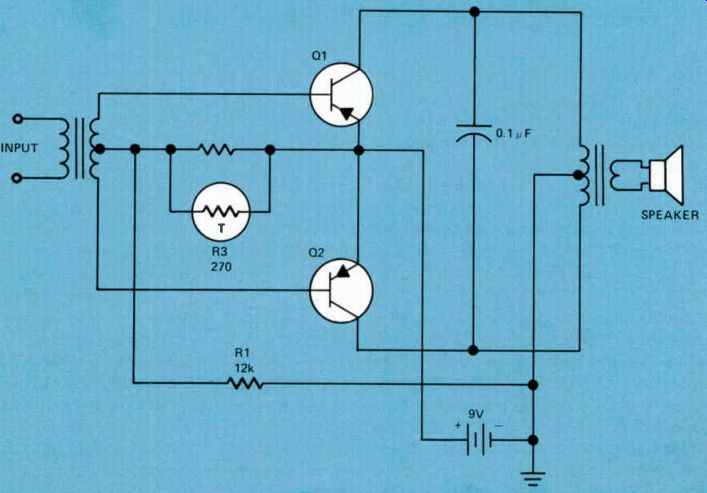
Figure 13. Class B push-pull PNP transistors.

Figure 14. A complementary symmetry push-pull amplifier.
Transformers can be built that have a reasonably good frequency response, but these transformers are expensive. Figure 14 shows a circuit that eliminates both the input and output transformers in a push-pull stage. This circuit uses a PNP and an NPN transistor, and is called a complementary symmetry push-pull amplifier. To make this circuit work, you need an NPN transistor and a PNP transistor that have essentially identical characteristics. Let's see how this circuit works.
First, notice that there is no negative connection from the power supply shown. This connection is simply omitted to simplify the diagram. When the diagram is drawn this way, you know that the negative connection from the power supply is to ground. Also, notice that at the input, we've shown only one input terminal. You know that the input signal is applied between this terminal and ground. Again, the second input is omitted for simplicity.
The stage preceding this push-pull output stage is a PNP driver stage. It is direct-coupled to the push-pull amplifier. Electrons flow from the negative side of the supply to ground, through the speaker, through the 270 ohm resistor R3, and through diode D1 and resistor R1, to the collector of the driver stage, where they fill holes arriving at the collector. This current flow through the speaker and through R3 develops the forward bias needed across the emitter-base junction of Q2. Notice that Q2 is a PNP transistor, so its base must be negative with respect to the emitter. The emitter connects through R2 to the emitter of Q1, which is an NPN transistor. The collector of Q1 is in turn connected to the plus side of the power supply.
The emitter of Q2 will be positive with respect to ground. The base will also be positive with respect to ground but it will be less positive than the emitter, so we'll have a for ward bias across the emitter-base junction. The diode D1 and R1 are in the circuit to ensure that the base of Q1 will be positive with respect to its emitter in order to forward bias the emitter base junction of this transistor.
With zero signal, since both transistors are forward biased, electrons will flow from ground to the collector of Q2 where they will fill holes arriving at the collector terminal.
Meanwhile, electrons will be leaving the emitter of Q2 creating the holes that flow through the transistor. The electrons leaving the emitter flow through R2 to the emitter of Q1. Since Q1 is an NPN transistor, the electrons flow through it to the collector and to the positive side of the supply.
This current flow will develop a voltage so that the emitter of Q1 is positive. Electrons will flow through the speaker into the plate of C1 marked with a - sign and out of the positive plate to charge C1 to the voltage between the emitter of Q1 and ground.
When the input signal swings in a positive direction, the current flow from ground through the speaker, through R3 and D1, and through R1, will increase. This will swing the base of Q2 in a positive direction, reducing the forward bias across the emitter-base junction of the transistor. Therefore, the number of holes flowing through the transistor will decrease, which means the number of electrons leaving the emitter of Q2 will decrease. At the same time, the base of Q1 will swing in a positive direction, increasing the forward bias across the emitter base junction of this transistor. Therefore, the current through Q1 must increase. This will cause electrons to flow from ground through the speaker and into the negative plate of C1, and out of the positive plate to Q1. This increase in current through the speaker produces a magnetic field in the speaker voice coil.
When the input signal swings in the negative direction, the current flow from ground through the speaker, R3, D1, and R1 will decrease. This will decrease the voltage drop across R3 so that the base of Q2 will become less positive. This will increase the forward bias across the emitter base junction of Q2. At the same time, the reduced current flow will reduce the positive voltage at the base of Q1, reducing the forward bias across the emitter-base junction of this transistor, causing the number of electrons flowing through it to decrease. Here, we have the opposite situation to what we had before in that we have the electron current through Q1 decreasing, but the hole current through Q2 increasing.
The increased number of holes flowing through Q2 will result in more electrons flowing from ground to the collector of Q2 and additional electrons flowing out of the emitter of Q2. Since the current of Q1 has dropped, these electrons will flow through R2 and into the positive plate of C1, and will begin to discharge this capacitor. Electrons will then flow out of the negative plate of C1 and through the speaker voice coil in the opposite direction.
This change in the direction of current flow through the speaker will set up a magnetic field around the speaker voice coil that has the opposite polarity. This changing magnetic field will cause the speaker voice coil to move in and out and will set the air in front and back of the speaker in motion. It is this motion of air columns that produce sound.
Inverse Feedback
We have already briefly mentioned inverse feedback. It is negative feedback that reduces the output. It also reduces distortion and improves the frequency response of an amplifier.
Negative feedback can be applied to the single-ended Class A power amplifiers shown in Figs.9 and 10 by omitting C2. C2 is the emitter bypass in the circuit.
In the circuit in Fig.9, if the input signal swings the base of Q1 in a positive direction, it will increase the forward bias across the emitter-base junction of the NPN transistor. This will cause the number of electrons flowing through the transistor and through R3 to increase. This will increase the voltage drop across R3, driving the emitter end in a positive direction, which will tend to reduce the forward bias across the emitter-base junction. This will tend to reduce the net effect of signal voltage between the base and the emitter and reduce the gain of the stage.
In the circuit in Fig.10, if the input signal of Q1 swings in a negative direction, it will increase the forward bias across the emitter-base junction of the PNP transistor. This will cause the number of holes that are crossing the emitter-base junction to increase, which will cause the electrons leaving the emitter and flowing through R3 to the positive side of the power supply to increase. This will increase the voltage drop across R3, driving the emitter end in a negative direction, which will tend to reduce the forward bias across the emitter-base junction.
In both cases, this negative, or degenerative, feedback tends to reduce the gain of the stage.
If either stage amplifies some particular frequency in the band more than it does another frequency, this feedback will be greatest at this frequency or band of frequencies. Therefore, the gain will be reduced most for these frequencies. This will tend to keep the overall gain of the amplifier constant over a wider frequency range.
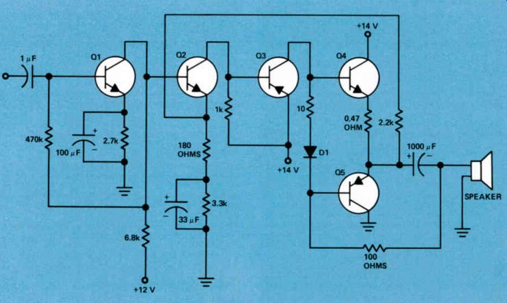
Figure 15. A three-stage negative feedback system.
A more elaborate feedback system where the signal is fed back three stages is shown in Fig.15. In this system, if the base of Q2 (an NPN transistor) is driven positive by the signal, the feedback signal drives the emitter positive, reducing the net effect of change in emitter base forward bias. Similarly, when the base of Q2 swings negative, the feedback signal drives the emitter negative, which again reduces the effect of change in the emitter-base bias. Let's trace the signal through the amplifier.
If the incoming signal swings the base of Q1 negative, current through Q1 will decrease so the voltage drop across the 6.8k load resistor will decrease. This causes the collector of Q1 and the base of Q2 to swing in a positive direction. When the base of Q2 swings positive, it will increase the forward bias across the emitter-base junction of the transistor so the current through Q2 will increase. This will cause the voltage drop across the 1-k collector resistor to increase so that the collector of Q2 will swing in a negative direction. Since Q3 is a PNP transistor, the increased voltage drop across the 1-k resistor will increase the forward bias across the emitter-base junction of Q3.
This will cause the collector current to increase. The collector current for this transistor flows from ground through the speaker, through the 100 ohm resistor, through the diode D1, and through the 10 ohm resistor to the collector, where the electrons fill holes arriving at the collector. This increased current flow will drive the base of Q4, which is an NPN transistor, in a positive direction. This will cause the current flow through this transistor to increase so that the current will flow through the speaker, into the 1000 uF capacitor, through the 0.47 resistor, and through the transistor. This causes the voltage across the capacitor to increase so that a positive signal is fed through the 2.2k resistor and back to the emitter of Q2. This will reduce the effect of the positive-going signal on the base of Q2.
When the input signal drives the base of Q1 positive, it will cause the current through this transistor to increase so the voltage drop across the 6.8k collector resistor will increase, swinging the collector of Q1 and the base of Q2 in a negative direction. This will cause the current flow through Q2 to decrease so that the voltage drop across the 1k resistor in the collector circuit decreases, which in turn decreases the forward bias across the emitter-base junction of the PNP transistor Q3. This causes the current through it to decrease, so that the current through the speaker, the 100 ohm resistor, D1, and the 10 ohm resistor decreases. This will increase the forward bias across the emitter-base junction of Q5 and reduce the forward bias across the emitter-base junction of Q4, so that the current through Q4 will go down but the current flow through Q5 goes up. This will cause the electrons that are leaving the emitter of Q5 to flow into the 1000 uF capacitor to reduce the charge on the capacitor. In other words, the voltage swings in the negative direction. This voltage is fed through the 2.2k resistor, back to the emitter of Q2. This will reduce the effect of the negative voltage applied to the base of Q2 by attempting to increase the forward bias across the emitter base junction of the transistor. Overall feed back of this type tends to flatten out the frequency response of the amplifier.
Another feedback circuit is shown in Fig.16.
Notice that in this circuit we have no output transformer but we do have an input transformer. Also notice that all three transistors are PNP transistors.
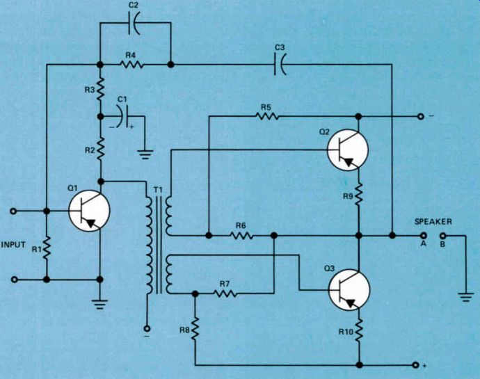
Figure 16. Three transistor amplifiers where there is no output transformer.
We are not going through all of the details of this circuit, but briefly with no input signal, the transistors Q2 and Q3 are biased so that the current flow through them is equal. Therefore, electrons will enter the negative terminal, and flow to the collector of Q2 where they will fill holes arriving there. Electrons will leave the emitter of Q2, flow through R9 and over to the collector of Q3 where they will fill holes arriving there. Electrons will leave the emitter of Q3 and flow through R10 to the positive side of the power supply. With zero signal applied, there will be no current flow through the speaker and the collector of Q3 will be at ground potential.
The windings of T1 are phased so that with a positive input to Q1, we'll get a negative signal on the base of Q2 and a positive signal on the base of Q3. Current through Q2 will increase; current through Q3 will decrease. Electrons will leave the negative terminal of the power supply to fill holes arriving at the collector of Q2. Some of the electrons leaving the emitter of Q2 will flow through R9 to the collector of Q3, but most will flow through the speaker, making terminal A of the speaker negative. This negative voltage is fed through C3 and C2 and R4 in parallel, back to the base of Q1 where it tends to reduce the input signal.
When the base of Q1 swings in the negative direction, the base of Q2 will swing in a positive direction and the base of Q3 in the negative direction. The number of holes flowing through Q3 will be greater than the number of holes flowing through Q2. Electrons will leave the negative terminal supply to fill holes arriving at the collector of Q2. Electrons will leave the emitter of Q2 and flow through R9 to the collector of Q3 to fill holes arriving there.
However, there will not be enough electrons leaving the emitter of Q2 to fill all the holes arriving at the collector of Q3 so electrons flow from ground through the speaker to terminal A and then to the collector of Q3. This will make terminal A of the speaker positive. This voltage is fed back to the base of Q1 to reduce the negative voltage fed to the base of Q1.
Feedback of this type from the output back to Q1 tends to make up for any lack of flat frequency response in T1. Sometimes transformers have a peak where a certain signal frequency will receive considerably more amplification than other signals. If this happens, the output signal will increase, resulting in increased feedback to Q1, which will tend to flatten out the frequency response. Transformers also have a tendency of falling off at low frequencies. They just don't work as well. When this happens, the feedback signal will decrease, and once again will tend to improve the frequency response of the amplifier.
IC Amplifiers When ICs were first used in audio systems, they were used as voltage amplifiers and the output of the IC was then fed to a power amplifier. Now, ICs are available that contain the entire audio system including the power amplifier. The one shown in Fig.17 is an example of such an IC.
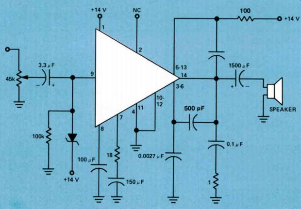
Figure 17. IC voltage amplifier and power amplifier.
This circuit is taken from an automobile receiver. In automobile receivers, compact size is very important. This particular receiver is a stereo receiver, which means there has to be two audio amplifiers. Therefore, any simplification that can be made in the amplifier helps to keep the receiver as small as possible.
In the circuit shown, the signal is taken from the volume control and fed through a 3.3 uF capacitor to terminal 9, which is the input to the integrated circuit. The output is taken off terminal 14 and fed through a 1500 uF capacitor to the speaker. The diagram shows all connections to the integrated circuits, but the manufacturer's service information does not show what is in it. As a technician, you will run into circuits of this type. If the amplifier fails to work, all you can do is check for the input signal to terminal 9. If it is normal, then check the components associated with the integrated circuit. If they are all good, you have to assume that the integrated circuit is defective and re place it.
In this particular integrated circuit, there are two differential amplifiers used as voltage amplifiers, and the output from the last one is fed to a power amplifier made up of an NPN and a PNP transistor connected as shown in Fig.14. All of this circuitry is inside the IC. If anything goes wrong with one of the components or transistors inside the IC, there is nothing you can do except replace the entire unit.
Summary
Single-ended power amplifiers are all Class A power amplifiers. They are used in applications where good quality is satisfactory, and economy is most important.
Push-pull audio amplifiers may be either Class A or Class B amplifiers. A push-pull amplifier has the advantage over a single ended amplifier in that the distortion is lower. Even order harmonic distortion is canceled in push-pull amplifiers. A Class B push-pull amplifier draws little or no current under zero signal conditions. Thus it is more efficient than a push-pull Class A power amplifier. This is particularly advantageous in portable equipment.
IC amplifiers that contain entire audio systems are made up of voltage amplifiers and a power amplifier. When a defect develops in part of an IC amplifier, all you can do is replace the unit.
Inverse feedback is used to reduce distortion and improve the frequency response of an amplifier. With inverse feedback, part of the amplified output signal is fed back to the input to oppose or reduce the effective input signal.
Self-Test Questions
10 In Figs.9 and 10, is T1 a step-up or a step-down transformer?
11 Is the signal current in the secondary of Ti in Fig.9 greater or less than the primary signal current?
12 When a signal is applied to Q1 and Q2 in the circuit shown in Fig. 12, what happens to the current through R2?
13 What is the advantage of using a Class B push-pull power amplifier such as shown in Fig.13 in a portable transistor receiver?
14 What are two advantages of eliminating the input and output audio transformers shown in Fig.13?
15 In Fig.14, if the input signal causes the current through Q1 to increase and the current through Q2 to decrease, where does the extra current required by Q1 come from?
16 In Fig.15, if the input signal causes the current through Q5 to increase, what is the polarity of the feedback signal back to the emitter of Q2?
17 If you have normal input to an IC amplifier such as shown in Fig.17, all operating voltages are normal, and the parts are good, but there is no output from the speaker, what should you do?
RADIO FREQUENCY AMPLIFIERS
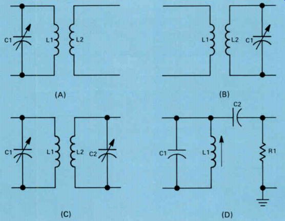
Figure 18. Four basic loads that might be found in RF amplifiers.
Radio frequency amplifiers are generally referred to as RF amplifiers. RF amplifiers can be divided into two types: voltage amplifiers and power amplifiers. The RF amplifiers in radio and television receivers will all be voltage amplifiers, whereas the RF amplifiers found in radio and TV transmitters will be power amplifiers.
In the amplifiers that you studied in the preceding sections, we found that we had a load in the output circuit of each stage. The load was in the collector circuit of the amplifiers using transistors and in the drain circuit of the amplifiers using FETs. In the case of voltage amplifiers, the load is usually a resistor, where as in the case of power amplifiers, the load is usually either the output transformer or the speaker. You will find a load in the output circuit of RF amplifiers, but in this case, the load is usually a resonant circuit. Most often, the resonant circuit will be a parallel-resonant circuit.
Four basic loads that you might run into in RF amplifiers are shown in Fig.18. In the one shown at (A), the load is a parallel-resonant circuit made up of L1 and C1. L1 is inductively coupled to L2 in order to feed the signal to the next stage.
In the circuit shown at (B), the load is L1. In this case it is not a resonant circuit but an inductance. However, L1 is inductively coupled to 1,2, which along with C1 makes up a resonant circuit.
In the circuit shown in Fig.18(C), we have two resonant circuits. L1 and C1 will be in the output circuit of the RF amplifier, and they form a parallel-resonant circuit. L1 is inductively coupled to L2 so that voltage is induced in series with each turn of L2. Since the voltage is induced in series with the various turns of the coil, L2 and C2 form a series-resonant circuit.
At first glance, you might think the circuit is a parallel-resonant circuit because it looks like the circuit made up of L1 and C1. Remember that the determining factor, whether the circuit is series-resonant or parallel-resonant, is how the voltage is applied to the circuit. The voltage is applied in parallel across L1 and C1, but it is induced in series with the turns of L2, which makes the circuit L2-C2 a series-resonant circuit.
In the circuit in Fig.18(D), we have a parallel resonant circuit made up of C1 and L1 as the load. The parallel-resonant circuit will act as a high resistance so that considerable signal voltage will be developed across it. This voltage is coupled through C2 to the following stage. You will run into all four types of loads shown in Fig. 18 in RF amplifiers and related circuits.
Some RF amplifiers are designed to operate over a band of frequencies. For example, the RF amplifier in the input of a radio receiver must be able to amplify signals over the entire AM broadcast band from 550 kHz to 1600 kHz. As you tune the radio across the band, the RF amplifier is tuned to operate at the frequency of the broadcast stations you wish to receive.
Some RF amplifiers, on the other hand, are designed to operate at only one frequency.
Before studying RF amplifiers in detail, let's learn a little more about resonant circuits.
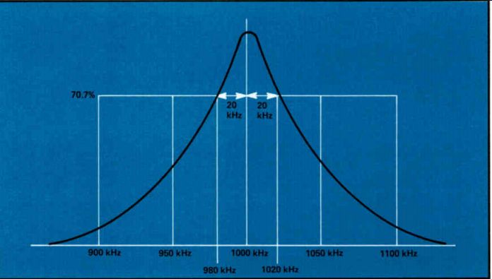
Figure 19. A response curve showing the two 70.7% points. The bandwidth
extends 20 kHz on each side of the resonant frequency.

Figure 20. The response curves at (C) show the effect of loading a parallel
resonant circuit as at (B).
Resonant Circuits
When we say a circuit is resonant, we mean that the inductive reactance in the circuit is exactly equal to and canceled by the capacitive reactance in the circuit. In the case of a parallel resonant circuit, the tank current will be at a maximum but the circuit itself will act like a high resistance. As a result, the current supplied to the resonant circuit by a generator connected across it will be at a minimum.
In the case of a series-resonant circuit, the resistance of the circuit will be at a minimum so that the current flow through it will be at a maximum. Current flow in a resonant circuit does not drop to zero immediately above and below the resonant point, but rather declines slowly as shown in Fig.19. Here we have a circuit that is resonant at 1000 kHz. Below the resonant point, the current drops off until at 900 kHz it is almost zero. Above resonance, it also drops off so that at 1100 kHz it is almost zero.
Since a resonant circuit responds to a band of frequencies around the resonant point, we say that this circuit has a bandwidth. Engineers have arbitrarily fixed the bandwidth of the circuit as the point where the voltage and current drop to 70.7% of the value at resonance.
This is called the half-power point. In the response curve shown in Fig. 19, the half-power points are 980 kHz and 1020 kHz. The band width of the circuit on each side of resonance is 20 kHz, so the total bandwidth of the circuit is 40 kHz.
You might wonder how this gets the name half-power point. At resonance, the power is equal to E x I. At the 70.7% point the power is equal to: P = 0.707 E x 0.707 I since, then
0.707 x 0.707 = 0.5 P= 0.707 x 0.707 xExI
= 0.5 xExI= 0.5 x p where P is the power at resonance.
We can change the bandwidth of a resonant circuit by loading the circuit. This is usually done by connecting a resistor across the circuit.
In Fig.20(A), we have shown a resonant circuit and curve 1 of Fig.20(C) represents the response curve of the circuit. In Fig.20(B), we've shown the same resonant circuit with a resistor connected across it and curve 2 of Fig.20(C) shows the response curve of the circuit with the resistor in parallel with it. The resistor lowers the peak of the response curve, and broadens the band of frequencies over which the response will be at least 70.7% of that at resonance.
In some applications, we may want a sharp response and a narrow bandwidth. In most communications receivers, we need a sharp, narrow response curve in order to separate stations operating close together. However, in TV, the response curves must be designed to pass a band of frequencies several MHz wide.
The coupling between resonant circuits will affect the response of the circuit. For example, in Fig.21 we have shown two resonant circuits.
The resonant circuit made up of C1 and L1 is a parallel-resonant circuit. However, L2 and C2 form a series-resonant circuit, since L2 is inductively coupled to L1 so that the voltage is induced in series with the turns of the coil. The voltage is induced in 12 by placing it near L1 so that the magnetic lines of force set up around L1 cut the turns of 12. If 12 is some distance from L1, so that only some of the magnetic lines of force set up by L1 cut 12, we say that the circuits are under-coupled or loosely coupled.
This will produce a response curve in the output like the one shown in Fig.22(A). If we bring 12 closer to L1, so that eventually we reach a point that all of the flux from L1 is cutting the turns of 12, we get a response curve like the one shown in Fig.22(B). We call this point critical coupling. At critical coupling, all the lines of flux produced by L1 are cutting 12.
If we bring the coils still closer together, we reach a point that is called over-coupled. By this we mean that the coupling is tighter than critical coupling and we'll get the double hump response curve shown in Fig.22(C). It is readily apparent that the bandwidth of the curve at (C) is wider than the bandwidth of the curve at (B).
If we want a still wider bandwidth, we can push the coils still closer together and then adjust one resonant circuit until it is resonant slightly below the original resonant point, and adjust the other resonant circuit so that it is resonant slightly above the original resonant point. This will give us a response curve like the one shown in Fig.22(D). In Fig.22(E), we have superimposed the four response curves so you can see what they look like in relation to each other. Notice that curve 1 is quite sharp, but its amplitude is less than curve 2. There are applications where it is worthwhile to take this drop in output to get a sharp response curve.
Normally the coils will be adjusted at least to critical coupling as shown by curve 2, and in several cases overcoupled as in curve 3. As an example, the response curve 2 might be adequate for AM broadcasting, but overcoupled coils like that shown at 3 might be required for FM because the FM signal requires a wider bandwidth than an AM signal.
In TV applications where an even wider bandwidth is needed, overcoupling and detuning the two circuits is used to get the wide bandwidth that is needed. Even though this results in a lower output as shown by curve 4 in Fig.22(E), we must resort to this technique in order to amplify all of the frequencies in the TV signal. We then make up for the drop in output by using additional amplifier stages.
As a technician, you will not have to be concerned about the coupling between coils in resonant circuits. The engineers that designed the set will take care of this in the design.
However, if you have to replace an RF transformer such as the one shown in Fig.21, it is important that you get either an exact duplicate replacement or a replacement that has the same characteristics as the original transformer. Otherwise, you'll change the bandwidth and gain of the amplifier.
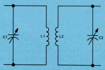
Figure 21. A schematic diagram of a double-tuned RF transformer.
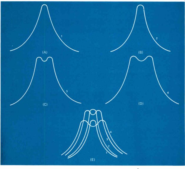
Figure 22. (A) An example of under-coupling, (B) critical coupling. (C)
and (D) overcoupling, and (E) a super-imposition of the curves.
Transistor RF Amplifiers
A typical RF amplifier that might be found in a radio receiver is shown in Fig.23. The circuit uses an NPN transistor in a common-emitter circuit.
L1 is a coil wound on a ferrite rod. A ferrite rod is a rod made of a powdered iron-type material held together by a suitable binder. L2 is wound on the same rod and is inductively coupled to Ll. This particular part is called a loopstick. In the first radios built with an inside antenna, the coil in the input to the RF amplifier stage was wound in the form of a loop. The passing signal from the broadcast station cut the turns of the loop and induced a voltage in each turn. This voltage was then fed to the RF amplifier. The antenna was called a loop antenna
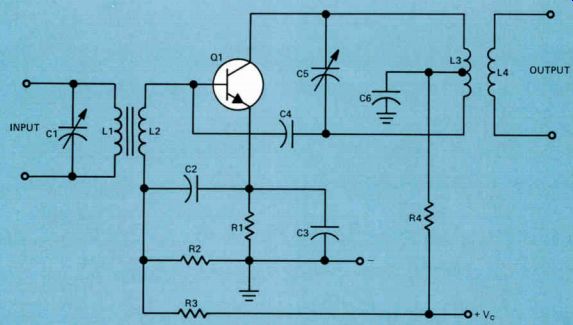
Figure 23. A transistor if amplifier.
The ferrite rod with the two coils wound on it replaced the loop antenna. Since this device looked like a stick and replaced the loop, the name loopstick came into use.
In the loopstick, the passing radio signals induced a voltage in the turns of L1. L1 is tuned to resonance by C I so that the voltage induced at the resonant frequency will cause a much higher current to flow in the resonant circuit than other frequencies. This in turn will mean that maximum signal voltage at the resonant frequency will be induced into 12.
L2 is inductively coupled to L1. 12 has fewer turns than L1 so there will be a current step-up, meaning that the current flowing in 12 will be higher than the current flowing in L1. This serves two useful purposes, it provides a higher current for the emitter-base circuit of the transistor Q1, and it prevents the transistor from loading the resonant circuit. If current through Q1 did load the resonant circuit excessively, it would lower the Q, broadening the circuit's response curve and reducing the selectivity.
The signal induced in 12 is applied to the base of the transistor and to the emitter through C2. C2 is selected to have a low reactance at the signal frequency. The varying emitter base current produced by the signal produces a high signal collector current, which is fed to the parallel-resonant circuit consisting of 1.3 and C5.
Notice that the collector voltage is applied to a tap on 12 through R4. C6 is connected between the tap and ground which holds the tap at signal ground potential. There will be a small voltage induced in the lower half of the coil which will be 180° out of phase with the signal voltage at the collector. This voltage is fed through C4 and back to the base. This is a neutralizing voltage and C4 is called a neutralizing capacitor.
We feed this signal back through C4 to prevent Q1 from oscillating. When a transistor oscillates, it begins generating a signal of its own. Q1 will oscillate because there is a high signal voltage developed across L3 between the collector and ground. There is a certain capacitance between the collector and base of the transistor. Some of this signal will be fed back into the base. The signal will be strong enough to develop a signal of its own. Thus, the signal fed from the collector to the base causes the base-emitter circuit to generate a signal, which in turn is fed to the collector and from the collector back to the base. Thus, the stage begins to oscillate and produces its own signal.
To prevent this, we feed a signal that is 180° out of phase with the signal at the collector through C4 and back into the base. This cancels or neutralizes the signal being fed from the collector to the base through the internal collector-base capacitance of Q1.
IA is inductively coupled to L3 so that the amplified output from the RF amplifier is fed on to the next stage.
Figure 24 is a schematic diagram of an RF amplifier using a junction field-effect transistor. Notice that the signal is picked up by the antenna and fed to L1, which is inductively coupled to L2. L2 and C1 form a series resonant circuit. C1 is adjusted so that the combination is resonant at the frequency of the desired station. The capacitance of C2 is so large that as far as the RF is concerned, it can be ignored. It is used to block the age (automatic gain control) voltage from ground so that it will not be shorted out. The age voltage is a negative voltage that is applied to the gate of the transistor. This voltage will vary to control the gain of the transistor, becoming more negative on strong signals and less negative on weak signals.
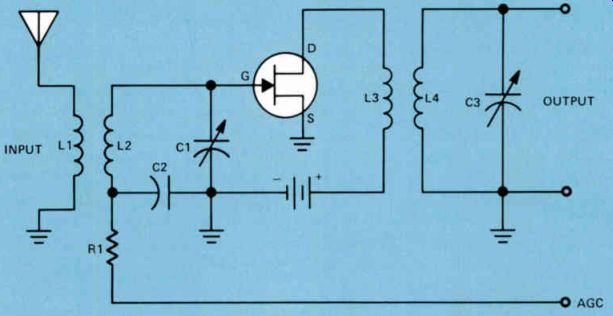
Figure 24. An if amplifier using a junction field-effect transistor
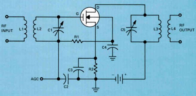
Figure 25. An RF amplifier using an insulated-gate field-effect transistor.
The varying signal applied between the gat and ground causes the current flow from the source to the drain of the transistor to vary.
This small varying signal fed to the gate con-trots a large varying current flow from source to drain, and this current in turn flows through L3. I2 is inductively coupled to IA which is tuned to resonance by C3. The amplified signal voltage appearing at the output is then fed on to the next stage.
In the circuit shown in Fig.24, there will be some reverse current flow across the junction of the transistor. This will have the effect of lowering the input resistance of the transistor, which in turn will lower the Q of the resonant circuit. This can be overcome by using an insulated-gate field-effect transistor in the circuit such as shown in Fig.25. The circuit here shows an n-channel depletion-type, insulated gate, field-effect transistor.
In the circuit shown, current flows from the negative side of the power supply, through R2 to the source of the transistor. It flows through the transistor to the drain, and then through 12 back to the positive side of the voltage source.
The gate is connected to the negative automatic gain control voltage through L2. The negative voltage applied to the gate will limit the width of the channel and control the resistance of the channel.
In operation, the RF signal is applied to L1. This may be from another RF amplifier or directly from the antenna. The signal current flowing through L1 induces a voltage in series with L2.
L2 and C1 form a series-resonant circuit. The resonant signal voltage is applied to the gate of the transistor and this voltage is applied in series with the negative agc voltage so it varies the negative voltage on the gate at an RF rate. The varying signal voltage causes the resistance of the channel to vary, causing the current flowing from the source through the transistor to the drain to vary. L3 and C5 form a parallel resonant circuit. This high-impedance circuit develops a high signal voltage due to the varying current flowing through it. L3 is inductively coupled to LA, and the output from LA is fed to the following stage.
A p-channel transistor can be used as well as an n-channel transistor in a circuit of this type.
Also the enhancement type of insulated-gate transistor could be used. However, it is likely that most RF amplifiers using an insulated-gate field-effect transistor will be depletion-type n channel transistors. Dual gate IGFETs are widely used as RF amplifiers. The signal is fed to one gate and the age voltage to the other.
One of the disadvantages of the insulated gate transistor is that it is easily damaged.
Simply removing or inserting the transistor in the circuit when the voltages are applied could destroy the transistor. High peak voltages build up in the gate circuit due to the very high resistance of the gate. Since the gate is actually insulated from the drain source by means of a layer of insulation, the input resistance of the gate is very high. Pickup from a nearby power line can induce a high enough voltage in a gate to destroy the transistor if the circuit is open.
I-F Amplifiers
Modern radio and television receivers are called superheterodyne receivers. In a super heterodyne receiver, the incoming signal is fed to an RF amplifier such as shown in the block diagram in Fig.26. The signal is amplified and fed to a mixer stage where it is mixed with a locally generated signal. This produces two new signals, one equal to the sum of the frequencies of the two signals and one equal to the difference. The difference frequency is fed to an amplifier called an intermediate frequency amplifier which is abbreviated i-f amplifier. The signal is still a radio frequency signal, but it has a lower frequency than the actual received signal. The signal is then fed to a detector, which separates the audio signal from the RF carrier. The detector gets its name, second detector, because in the early days of radio, the mixer was called the first detector. The audio signal from the second detector is then fed to low-frequency voltage amplifiers and finally to a power amplifier.
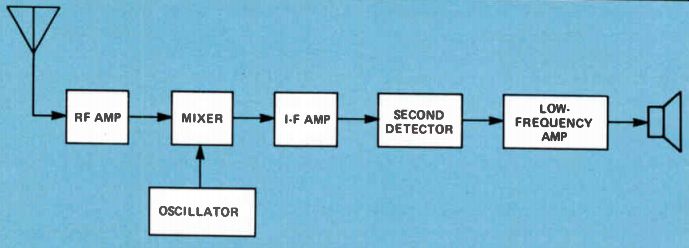
Figure 26. A block diagram of a typical super-heterodyne receiver.
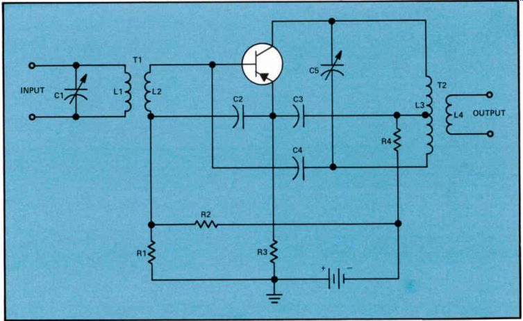
Figure 27. A typical transistor i-f amplifier using a PNP transistor.
The reason for converting the incoming signal to a low-frequency signal is to improve the receiver selectivity. Consider two stations, one operating on 1500 kHz and the other on 1450 kHz. The frequency difference is 50 kHz, which is just a little more than 3% of 1500 kHz. After the two signals have been converted to a lower RF frequency (455 kHz is a common i-f frequency), the 50 kHz separation between the two stations represents a frequency difference of almost 11%. The i-f amplifier can separate the two signals, whereas an RF amplifier operating at 1500 kHz would not be able to do so.
All modern receivers are superheterodyne receivers. AM broadcast receivers today use an i-f of 455 kHz. Automobile receivers frequently use an i-f of 262 kHz. Some older home-type receivers use this frequency, and 175 kHz was also used at one time. The important thing to remember is that an i-f amplifier is an RF amplifier operating at a low fixed frequency.
A typical i-f amplifier using a PNP transistor is shown in Fig.27. C1 and L1 form a parallel resonant circuit that is resonant at the intermediate frequency. They are part of the collector circuit of the mixer stage. L2 is inductively coupled to L1 so a signal is induced in L2 that is applied to the base of the transistor and to the emitter through C2, which has a low reactance at the i-f frequency.
The signal applied between the base and emitter causes the number of holes flowing through the transistor to vary. This causes the number of electrons flowing from the negative terminal of the power supply through R4 and the upper half of L3 to the collector, to fill the holes arriving at the collector to vary. IA is inductively coupled to L3, so a signal is induced in this winding that can be fed to a second i-f amplifier or to the detector stage. C4 provides neutralization that feeds a signal back into the base, which is 180° out of phase with the signal fed from the collector, to the base through the internal collector-to-base capacitance. The neutralizing signal cancels the feedback through the collector-to-base capacitance and prevents oscillation in the stage.
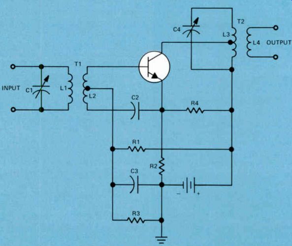
Figure 28. Transistor i-f amplifier using an NPN transistor.
Electrons leaving the emitter of the transistor to form holes flow through R3 to ground. In doing so, they develop a voltage drop across R3 having a polarity such that the emitter is negative with respect to ground. You will remember that this resistor is put in the circuit for bias stabilization to prevent thermal runaway of the transistor. R2 and R1 are selected so that the junction of the two resistors is more negative than the emitter of the transistor. The base of the transistor connects to the junction of R1 and R2 through L2 so the base will be negative with respect to the emitter, which places a forward bias across the emitter-base junction of the transistor.
Another transistor i-f amplifier is shown in Fig.28. This amplifier uses an NPN transistor whereas the one shown in Fig.27 uses a PNP transistor. In addition to the different transistor types, the method of obtaining neutralization is somewhat different. Notice the resistor in the emitter circuit, R2. This resistor is not by passed; therefore, a signal voltage will be developed across it. The signal voltage is fed through C2 into the lower end of the coil L2. The center tap of L2 is at signal ground potential because C3 has a low reactance at signal frequency.
The lower end of L2 is inductively coupled to the upper end so that a voltage is induced in the upper end of the coil 180° out of phase with the signal fed into the lower end through C2.
This voltage is fed to the base, neutralizing any signal voltage fed from the collector back to the base through the transistor itself.
Notice that the collector is connected to a tap on coil L3. The output resistance of the transistor is comparatively low, and by feeding the collector into a tap in the coil in this manner, we prevent loading of the parallel-resonant circuit made up of L3 and C4. Loading would reduce the selectivity of the circuit.
IC Amplifiers
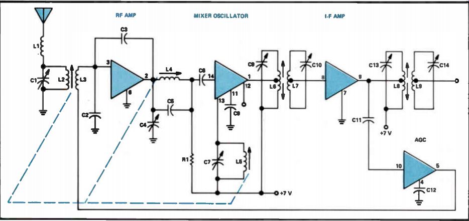
Figure 29. In the circuit shown, a single IC contains the RF amplifier,
the mixer-oscillator, the i-f amplifier, and the agc.
You might wonder if integrated circuits are used as RF and i-f amplifiers. The answer to this is yes. As a matter of fact, they are widely used in both radio and TV receivers.
In Fig.29 we show what can be accomplished with a single integrated circuit. Here, we have a 14-pin IC that is used as the RF amplifier, the mixer-oscillator, the i-f amplifier, the age detector, and the age amplifier. In fact, this IC could be used along with a diode as a detector and the IC shown in Fig.17 to form a complete receiver.
The coils L2-L3, L4, and L5 are all adjustable by a single adjustment. Changing these coils tunes the receiver across the standard AM broadcast band.
The signal picked up by the antenna is fed to the parallel-resonant circuit consisting of L2 and C1. The high circulating current in L2 induces a voltage in L3, which is fed to terminal 3 of the RF amplifier. The signal is amplified and fed through L4 to terminal 14 of the mixer oscillator. Also notice that a signal from the output of the RF amplifier is fed through C3 back to the input to neutralize the RF amplifier. In the mixer stage, the incoming signal is converted to 455 kHz, which is the i-f. The i-f signal is fed to pin 8 of the IC, where it is amplified and fed to the parallel-resonant circuit made up of C13 and L8. L9 is inductively coupled to L8, so a strong circulating signal is induced in the series resonant circuit made up of L9 and C14.
This signal can then be fed to the second detector.
Part of the signal from the output of the i-f amplifier is fed from pin 9 through C11 to the age detector and amplifier. In this stage a negative signal voltage, which depends upon the strength of the incoming signal, is developed, amplified, and fed back to the RF amplifier to control the gain of it. The stronger the signal, the greater the negative voltage developed and the more the gain of the RF amplifier is reduced.
ICs such as the one shown in Fig.29 are widely used because they are relatively inexpensive to manufacture. The assembly of the equipment is simple because the one part re places a number of discrete parts.
Summary
The RF amplifiers we discussed in this section are all voltage amplifiers. They are designed to take a weak radio frequency signal and amplify it into a stronger signal.
RF amplifiers have a load in the output circuit. In most cases, the loads will be some form of resonant circuit. An i-f amplifier is an intermediate frequency amplifier. It is an amplifier that operates at a relatively low radio frequency. In addition, since all incoming signals picked up by the radio are converted to the same intermediate frequency, the i-f amplifier is designed to operate at a fixed frequency. Its purpose is to improve the selectivity of the receiver. Selectivity is the ability of the receiver to separate signals operating on frequencies relatively close together.
Self-Test Questions
18 What do we mean by the bandwidth of a circuit?
19 Name two methods that can be used to increase the bandwidth of the circuit.
20 What do we mean by critical coupling?
21 What is the name given to C4 in the circuit shown in Fig.23?
22 Why is C4 necessary in the circuit shown in Fig.23?
23 What do the letters age in the circuit shown in Fig.24 stand for?
24 What is the advantage of using an insulated-gate field-effect transistor as an RF amplifier when compared to a junction field-effect transistor?
25 What is the i-f frequency used in the modern AM broadcast receiver?
26 What is the i-f used in many automobile receivers?
27 In the circuit shown in Fig.27, what purpose does C4 serve?
28 In the circuit shown in Fig.28, why is the collector fed to a tap on L3?
29 How many integrated circuits are used in the circuit shown in Fig.29?
-----------------
LOGARITHMS AND DECIBELS
If we feed a signal of 1 microvolt into an amplifier stage and we have a signal of 100 microvolts in the output, the gain of the stage is 100 divided by 1 = 100. This is one way of measuring the gain of a stage. Another method is to measure it in units called the decibel. The decibel is a logarithmic ratio. It is a ratio that is based on logarithms. Therefore, before we can understand what a decibel is, we must first learn something about logarithms.
There are two important types of logarithms in use today. One is called a common logarithm and the other a natural logarithm. Common logarithms are based on the number 10. This is the type of logarithms that you will study and use now.
The Theory of Logarithms
The basic idea of logarithms come from the fact that any number can be expressed as the power of another number. The power of a number is the product of a number multiplied by itself a given number of times. The first power of a number is the number itself; the second power is the number multiplied by itself; the third power is the number multiplied by itself twice, and so forth.
This is easiest to understand by taking an example. In the system of common logarithms, we express all numbers as a power of ten.
Therefore, we will use 10 as our example. The number 10 itself is equal to 10 to the first power. This can be written 10 ^1. The number 100 is equal to 10 x 10. This is 10 to the second power and can be written 10^2. Similarly, 1000 is equal to 10 x 10 x 10, which is 10 to the third power and can be written 10^3. The number 10,000 is 10^4. Since 10 x 10 x 10 x 10 is equal to 10,000, or 10^4.
Now, as we have said, 100 is 10 to the second power. The logarithm of 100 is simply the power to which 10 must be raised to give us 100. The number 10 must be raised to the second power (102) to give us 100. Therefore, the logarithm of 100 is 2. Similarly, the logarithm of 1000 is 3, and the logarithm of 10,000 is 4. The logarithm of 10 is 1.
This is not very complicated when the number is an exact power of 10. But let us consider the numbers between 10 and 100. It is a little more difficult to see how a number between 10 and 100 can be expressed as a power of 10.
Actually, this is quite difficult to work out mathematically, but it can be done. Fortunately, all these values have been worked out and are available in tables called logarithm or log tables. If you want to know the logarithm of a number, you simply refer to the table. For example, the logarithm of the number 2 is 0.301.
This means that if it were possible to multiply the number 10 by itself 0.301 times, the product would be 2. This can be written 10^3. 3 ' 3'. The exponent (or power) 0.301 is called the logarithm.
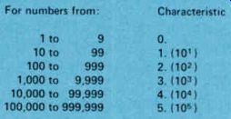
Figure 30. The characteristics of numbers from 1 to 999,999
Now let's take the numbers 20 and 200. The logarithm of 20 is 1.301 and the logarithm of 200 is 2.301. Notice that in the three logarithms for 2, 20, and 200, the figures to the right of the decimal point remain the same. The figures to the left change. The logarithm can be divided into two parts. The part to the left of the decimal point is called the characteristic, and the part to the right of the decimal point is called the mantissa.
For any number having the same digits, the mantissa does not change. For example, the mantissa of 2, 20, 200, 2000, 20,000, and 200,000 is always 0.301. However, the characteristic changes. The characteristic for 2 is 0, for 20 is 1, for 200 is 2, for 2000 is 3, and for 20,000 is 4.
Notice that the characteristic is always one number smaller than there are whole numbers in the original number. For example, in the number 2000 there are four numbers and the characteristic is 3.
The chart given in Fig.30 gives you the characteristics of the numbers you are likely to encounter.
We mentioned earlier that you can find the logarithm of a number by looking it up in a table of logarithms. You will find a table of logarithms in any good math reference book. A log table generally lists the numbers from 10 to 99 in the left column, which is usually headed with the letter N. To the right, there will be 10 additional columns with headings from 0 to 9. If you want to look up the logarithm of the number 25, you find the number 25 in the N column and then look in the first column which will be headed 0 and find that the logarithm is 0.3979. If you want to look up the logarithm of the number 255, you find the number 25 in the N column, and then move over to the column under the heading 5, and find that the logarithm is 0.4065. Notice that the log table gives only the mantissa of the number. You have to determine the correct characteristic yourself. This is easy to do because the characteristic is always one less than the number of whole numbers in the number. Also, the table given in Fig.30 will tell you that for numbers from 100 to 999, the characteristic is 2. Therefore, the characteristic for the number 255 is 2.
You can also find the logarithm of a number using a slide rule that has an L scale. However, this is not as accurate as using a log table, but often it is satisfactory. Today, with the availability of low-cost hand-held scientific calculators, both the log table and the slide rule are obsolete. Most scientific calculators have provisions for giving you the logarithm of a number rapidly and more accurately than you can get it from a log table.
The Decibel
Many years ago, engineers working on telephone installations introduced the unit of power measurement called the bet. This unit of measurement is named for Alexander Graham Bell, the inventor of the telephone. The bel was introduced as a unit of measurement because engineers and scientists discovered that the human ear responds to variations of loudness in a logarithmic manner. Therefore, it is convenient to have a unit that can be used to express the ratio between the power of two signals in a logarithmic manner. The bel is simply the logarithm of the ratio of the power of two signals.
For example, if we have a signal power of 100 watts and another signal power of 10 watts, and we wish to express the ratio of these two signals in bels, we would use the formula: bels = log LF- 1 P2 Substituting 100 watts for P1 and 10 watts for P2, we would get: 100 bels = log 10 = log 10 Now, the log of 10 is 1, so this power ratio is equal to 1 bel. In other words, a power ratio of 100 watts to 10 watts, which is a ratio of 10 to 1, is equivalent to 1 bel. Thus, the power ratios of 10 watts to 1 watt and 1000 watts to 100 watts are both power ratios of 10 to 1, so they also represent a change in power of 1 bel.
The bel proved to be too large a unit to handle easily, so another unit, 1/10 the size of the bel, was introduced. This unit is called the decibel, which is abbreviated dB. Thus, the commonly used measuring unit is the decibel; the prefix deci means 1/10. A power ratio in decibels is defined as: dB = 10 log - P1 P2 which simply means that the ratio of two powers expressed in decibels is equal to 10 times the logarithm of the ratio of the two powers.
You will notice that the above relationship refers to power ratios only. It is common in electronic work to use voltage ratios, especially when calculating or discussing the gain of amplifiers. When the ratio between two voltages is calculated in decibels, we must modify the decibel equation to take care of the fact that the power ratios are proportional to the squares of the voltage ratios, since P = E2 ÷ R. The formula to express voltage ratios in decibels is:
dB = 20 log – E1 E2
It is important to keep in mind that the voltage formula can be used only when the resistances of the two circuits being compared are equal. If we are trying to compare voltages developed across resistors of unequal value, we must convert the voltages to the power developed across the resistor and then use the power formula Using the Decibel It so happens that the smallest amount of change in sound level that can be distinguished by the average human ear is 1 dB with a sine wave input or 3 dB on complex waves such as the average human voice.
Because the decibel is such a convenient unit for expressing changes in sound level, manufacturers of audio equipment have for some time used it in describing the response of their amplifiers. This practice has generally spread into describing the performance of many amplifiers.
Let us see how the decibel can be used to describe the response of an amplifier. You will remember that we said that engineers arbitrarily selected the 0.707 voltage points, or the half power points, to describe the bandwidth of an amplifier. At the half-power point, we have a ratio of 1 to 0.5 because 0.5 is half of 1. In dB this is:
1 dB = 10 log - = 10 log 2 0.5
The log of 2 is 0.301; thus, the power ratio is: dB = 10 x 0.301 = 3 (approximately) Thus, at the half-power point, the power in the circuit is down 3 dB from what it is at the maximum power or resonant point.
Another way in which the decibel is used is in expressing attenuation of certain signals. For example, we mentioned that amplifiers frequently generate harmonics. While this is a problem in audio amplifiers because it introduces distortion, it is an even greater problem in radio frequency transmitters because it results in an extra or spurious signal being transmitted. For example, suppose a radio station transmitting in the standard broadcast band has a power output of 1000 watts. Suppose further that the second harmonic radiation is down 30 dB. This means that the second harmonic radiation is 30 dB less than the fundamental radiation. But just how much is 30 dB? It actually represents the power ratio of 1000 to 1. This means that if the power output on the fundamental is 1000 watts, the power output in the second harmonic is actually only 1 watt.
The table in Fig.31 gives the decibel values corresponding to voltage and power ratios.
From this you can see that if an amplifier has a voltage gain of 40 dB, the output signal will be 100 times the input signal.
If your primary intention is to go into radio TV servicing, you will seldom, if ever, have to calculate decibel values corresponding to voltage or power ratios. However, if you intend to go into communications or industry as an electronics technician, you should be able to calculate both voltage gain and power ratios in decibels.
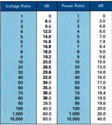
Figure 31. Decibel values corresponding to voltage and power ratios.
Summary
A common logarithm is the power to which 10 must be raised to equal a number. For example, 10^2 = 100 and 10^3 = 1000. A logarithm is made up of two numbers, a whole number to the left of the decimal point which is called characteristic and a decimal number to the right which is called a mantissa. The characteristic is always one less than the total number of digits in the number. For example, the characteristic of all numbers between 10 and 99 is 1, the characteristics of all numbers between 100 and 999 is 2 and the characteristics of all numbers between 1000 and 9999 is 3.
The mantissa of the logarithm of a number can be found by looking it up in the log table. For example, a log table will give the mantissa of the number 2 as 0.301. The logarithm of 2 is 0.301. The number 20 has the same mantissa as 2, but the characteristic is 1, so the log is 1.301. The logarithm of 200 is 2.301.
An easier way to find the logarithm of a number is with a pocket calculator. The calculator will give you both the characteristic and the mantissa of the number with better accuracy than you can obtain with most log tables.
The decibel is a logarithmic ratio that was originally developed to express the ratio between two powers. The power ratio in decibels is: P1 dB = 10 log – 2
The ratio between two voltages can also be expressed in decibels when the resistances of the two circuits being compared are equal. The formula is: dB = 20 log - El E2
Self-Test Questions
30 What is a common logarithm?
31 What is the part of the logarithm to the left of the decimal point called?
32 What is the part of the logarithm to the right of the decimal point called?
33 What is the characteristic of numbers from 100 to 999?
34 If the logarithm of 7 is 0.8451, what is the logarithm of 700?
35 What is the decibel?
36 If the power output from an amplifier drops from 1000 watts to 100 watts, what is the change in decibels?
ANSWERS TO SELF-TEST QUESTIONS
1 They are in phase. The signal under goes a 180° phase shift in each stage so the total phase shift is 360°, resulting in the output signal being in phase with the input signal.
2 It will swing in the negative direction.
There will be a 180° phase shift in Q1.
3 R5 is used to develop a reverse bias between the gate and the channel.
The current flowing through R5 will develop a voltage having a polarity such that the source end is positive.
This means the entire channel will be positive with respect to ground. The gate connects to ground through R4 and there is no current flow through R4 and no voltage drop. This means the channel will be positive with respect to the gate, or in other words, the gate will be negative with respect to the channel.
4 Replace the IC.
5 The + sign indicates a noninverting input. That means the signal fed into this input will produce an output signal that is in phase with it. The - sign indicates an inverting input. The out put signal will be 180° out of phase with the input signal fed into this input.
6 Q3 is an emitter follower.
7 The letter A indicates the gain of the amplifier.
8 The gain of the circuit is determined by the ratio of R2 to R1.
9 Two. Q 1 and Q2 form one differential amplifier and Q4 and Q5 form a second.
10 Step-down transformers. Step-down transformers are used to match the high impedance of the output stage to the low impedance of the speaker voice coil.
11 In a step-down transformer the secondary current is always greater than the primary current.
12 It remains constant. If the current through Q1 increases, the current through Q2 will decrease an equal amount so that the current through R2 remains essentially constant.
13 When the input signal is zero, the transistors Q1 and Q2 draw little or no power. This will result in improved battery life.
14 The frequency response of the amplifier will be improved and the cost will be reduced by the elimination of the two transformers.
15 From C1. C1 simply charges to a higher voltage and supplies the extra electrons needed by Q1.
16 Negative. If the current through Q5 increases, the electrons must come from the 1000 uF capacitor, which will tend to discharge the capacitor and produce a negative signal, which is fed back to the emitter of Q2.
17 Replace it. If the input signal is normal and all parts and operating voltages are correct, the IC must be defective.
18 The bandwidth of the circuit is generally defined as the frequency between which the output voltage is 0.707 or 70.7% of the maximum voltage obtained at resonance.
19 The bandwidth can be increased by overcoupling and by loading the resonant circuits.
20 Critical coupling is that point where the lines of flux produced in the primary winding of the transformer cut the turns of the secondary winding of the transformer.
21 C4 is a neutralizing capacitor.
22 Energy from the collector of Q1 will be fed back to the base through the collector-to-base capacity. This signal could cause Q1 to begin generating its own signal, which we call oscillating. The signal fed through C4 has the opposite polarity to the signal fed from the collector to the base of Q2 through the collector-to-base capacity and cancels it.
23 AGC stands for automatic gain control.
24 There is no current flow through the gate of the insulated-gate field-effect transistor, and therefore, it does not load the resonant input circuit. There is some current flow to the gate of a junction field-effect transistor, which will have some loading effect on the resonant circuit, which will reduce the selectivity of the circuit.
25 455 kHz.
26 262 kHz.
27 C4 is a neutralizing capacitor.
28 To reduce the loading on the resonant circuit.
29 1.
30 A logarithm is the power to which 10 must be raised to express another number.
31 The part of the logarithm to the left of the decimal point is called the characteristic.
32 The part of the logarithm to the right of the decimal point is called the mantissa.
33 Two. The characteristic of a number is one less than the total digits in the number.
34 2.8451. Both 7 and 700 will have the same mantissa in their logarithm. The difference is in the characteristic.
Since 700 has three digits, the characteristic must be 2.
36 The decibel is 1/10th of a bel. A bel is the logarithm of the ratio between two numbers.
36 The ratio of 1000 watts to 100 watts is 10 to 1. Thus, 1000 ± 100 is 10. The logarithm of 10 is 1; therefore, this change represents a change of 10 decibels.
LESSON QUESTIONS
This is Lesson Number 2230.
Make sure you print your name, student number, and lesson number in the spaces provided on the Lesson Answer Form. Be sure to fill in the circles beneath your student number and les son number.
Reminder:
A properly completed Lesson Answer Form allows us to evaluate your answers and speed the results and additional study material to you as soon as possible. Do not hold your Lesson Answer Forms to send several at one time. You may run out of study material if you do not send your answers for evaluation promptly.
1. During the negative half-cycle of a sine wave signal fed to the amplifier in Fig.1, which way will the collector voltage of Q1 and Q2 swing?
a. Q1 negative, Q2 negative.
b. Q1 positive, Q2 positive.
c. Q1 negative, Q2 positive.
d. Q1 positive, Q2 negative.
2. During the negative half-cycle of a sine wave signal fed to the amplifier in Fig.2, which way will the collector voltage of Q1 and Q2 swing?
a. Q1 negative, Q2 negative.
b. Q1 positive, Q2 positive.
c. Q1 negative, Q2 positive.
d. Q1 positive, Q2 negative.
3. If in the operational amplifier circuit shown in Fig.7(A), A equals 1000, R1 equals 5000 ohms, and R2 equals 50,000 ohms, the gain of the amplifier is:
a. 10.
b. 100. C. 1000.
d. 10,000.
4. When a signal is applied to a class A power amplifier such as shown in Fig.9, the aver age collector current:
a. Increases.
b. Decreases.
c. Remains the same.
d. Drops to zero.
5. What is the advantage of the class B push pull amplifier shown in Fig. 13 over the class A push-pull amplifier shown in Fig.12?
a. Has higher power output.
b. Uses PNP transistors.
c. Has lower distortion.
d. Has lower power consumption.
6. A positive-going signal fed to the input of the circuit shown in Fig.14 will cause the current through:
a. Q1 and Q2 to increase.
b. Q1 and Q2 to decrease.
c. Q1 to increase, Q2 to decrease.
d. Q1 to decrease, Q2 to increase.
7. The most important effect noticed when the coupling between the coils of an RF transformer is increased beyond critical coupling is that:
a. The output will increase.
b. The output will decrease.
c. The bandwidth will decrease.
d. The bandwidth will increase.
8. Transistor RF amplifiers are usually neutralized to:
a. Increase the gain.
b. Decrease the gain.
c. Prevent oscillation.
d. Reduce power consumption.
9. In the circuit shown in Fig.29, which is neutralized?
a. The RF amplifier.
b. The mixer-oscillator.
c. The i-f amplifier.
d. The agc detector amplifier stage
10. The input and output impedance of a certain amplifier are both 500 ohms, and the gain of the amplifier is 20 dB. If an input signal of 1 volt is fed into the input, what would you expect to find in the output?
a. 1 volt.
b. 10 volts.
c. 20 volts.
d. 100 volts.
NOTES Please use this page to record any notes you may want to review during your studies.

NRI Schools
THE ERROR OF HASTE
The fable of the hare and the tortoise is more than an interesting childhood story - it carries an important message we sometimes forget in this age of speed.
The hare, you will recall, started off in great haste. Soon it was so far ahead of the slow-plodding tortoise that it became overconfident and took a nap. The tortoise kept going steadily and won the race.
Haste does not always mean progress. Too often it leads instead to errors, to actual waste of time and energy, and even to complete failure, as in the case of the hare.
We must learn to work and wait. Take time for all things, because time often achieves results that are obtainable no other way. Shakespeare expressed it thus: "Wisely and slow; they stumble who run fast." More emphatic still was Benjamin Franklin, who said: "Great haste makes great waste." Don't risk the dangers of haste. Keep going steadily like the tortoise, and you'll approach your goal steadily, inevitably.
| Top of Page | PREV | NEXT | Article Index |