Whether you are interested in analog or digital electronics, small or large projects, or a range of project types, the value of test equipment is something that should not be underestimated. In an ideal world there would be no need for test equipment at all. Projects would always work first time, and would continue to do so indefinitely. In the real world we are fallible, and do make mistakes when building projects. I constructed an embarrassingly large number of projects before one worked first time!
"Dud" components are very rare these days. The large numbers of dubious semiconductors that were once on sale as legitimate components seem to have disappeared from the market, or are sold as "untested" devices in bargain packs.
Nevertheless, faulty components can still slip through testing procedures, or components that were originally serviceable can fail in use.
Mistakes in the component layout, short circuited tracks on a printed circuit board, and other faults of a largely mechanical nature can often be traced by a visual inspection of the circuit board etc. Some faults are not traceable in this way though, and tracking down a faulty component can be very difficult without the aid of suitable test gear. It can become a matter of replacing components in the hope that this substitution testing will bring to light the faulty component sooner rather than later!
AF Generator
A number of simple but useful test gear projects are described in this guide, starting with some audio test equipment in this Section. What could reasonably be regarded as the most essential piece of audio test gear is an audio signal generator.
The unit described here has an operating frequency range of less than 20Hz to more than 20kHz in three ranges. These are 20Hz to 200Hz, 200Hz to 2kHz, and 2kHz to 20kHz. Each range is actually slightly wider than quoted above so that there is a slight overlapping of ranges, and no risk of any gaps between them. Both sinewave and squarewave outputs signals are available, with an output level of about 2.8 volts peak to peak in both cases. In terms of RMS voltage, this works out at about 1 volt RMS for the sinewave signal. There is a volume control style variable attenuator plus a -20dB switched attenuator. The latter reduces the output voltage by a factor of ten, and makes it easier to accurately set a specific output level when low output voltages are required.
The sinewave output is the one that is used for most audio testing. The important attribute of a sinewave is that it contains only the fundamental frequency. Other repetitive waveforms contain harmonics (multiples of the fundamental frequency). With the squarewave output signal for example, there are strong odd order harmonics (i.e. three times, five times, seven times the fundamental frequency, etc.). Obviously for some types of testing, the purity of the output signal is not of great importance, and neither is the precise output frequency. In other cases they are both crucial, and this includes frequency response testing, which is one of the most common uses of audio signal generators. Squarewave test signals are mainly used in conjunction with an oscilloscope.
Distortion of the wave shape can reveal irregularities in the frequency or phase response of a circuit, as well as other aspects of performance such as "ringing". Squarewave testing is a subject that we will return to later in this Section.
Wien Bridge
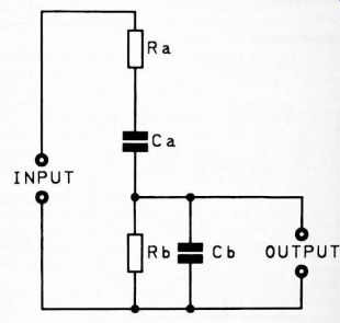
Fig. 1.1 The Wien network circuit
For as long as I have been involved in electronics (about 25 years or so) the standard form of audio signal generator seems to have been a Wien Bridge type having thermistor stabilization. The advantages of this form of oscillator are its excellent performance coupled with extreme simplicity. The only real drawback is that the thermistor to provide the gain stabilization is relatively expensive, and is not the most widely available component. It is well worth the trouble and expense though. Oscillators using a good stabilizing thermistor can easily provide distortion levels that are only a minute fraction of 1%, and maintain the output level to well within plus and minus 1dB over a very wide frequency range. A Wien Bridge oscillator with thermistor stabilization might not be the latest thing in modern technology, but it still provides a level of performance that can not easily be bettered.
A Wien network consists of two resistors and two capacitors connected in the manner shown in Figure 1.1. It can be regarded as a phase shift network, and at a certain frequency the input and output will be in phase. For the mathematically minded, this frequency is obtained using this formula:
f = 1/2 pi Ca Ra
It is assumed here that Ra = Rb, and that Ca = Cb, which is normally the case for a Wien network used in -a real-world application. There is a loss of about 10 dB (i.e. the output signal voltage is about one-third of the input signal level) at the zero phase shift frequency. In theory, all that is needed in order to produce a high quality sinewave oscillator is a setup of the type outlined in Figure 1.2. Here the Wien network is placed between the output and non-inverting input of an operational amplifier. It therefore provides positive feedback at the zero phase shift frequency, and provided the losses through the network are matched by the voltage gain through the amplifier, there will be sufficient feedback to sustain oscillation at this frequency.
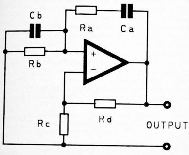
Fig. 1.2 The standard Wien Bridge oscillator configuration.
In reality things are a little more tricky than this. Setting the voltage gain of the amplifier at three times by giving negative feedback resistors Rc and Rd the right values is not too difficult, but will not be satisfactory in practice. If the tolerances of these components should result in slightly too little gain the circuit will fail to oscillate. If their tolerances should result in marginally too much gain, excessively strong oscillation will result. This will cause the output signal to become clipped, and strong distortion products will result.
In fact the output signal would be closer to a squarewave than the required sinewave signal! One way around the problem is to use a gain control to permit manual adjustment of the oscillation level. In practice this does not work very well as changes in the frequency control, variations in the loading on the output, etc., make it necessary to almost continuously trim the gain control for the correct output level.
Some form of automatic gain control is much more satisfactory, and the most simple method is to replace feedback resistor Rd with a special form of thermistor. Most thermistors are designed to respond to the ambient temperature, but the type required for this application is the so-called "self heating" variety. These are contained in an evacuated glass envelope so that, as far as possible, they are isolated from the ambient temperature. The type used in this application are the usual negative temperature coefficient thermistors, which simply means that increased temperature gives reduced resistance. The temperature of the device is largely a function of the current which flows through it.
In this case the current flow depends on how strongly (or otherwise) the circuit is oscillating. Strong oscillation forces relatively large currents through the device, while with very weak oscillation there is virtually no current passed through it.
Initially the thermistor is cold, it has a high resistance, and there is little negative feedback. This gives strong oscillation, as the voltage gain of the amplifier is inversely proportional to the amount of feedback. This oscillation forces relatively large currents through the thermistor, which consequently heats up and has greatly reduced resistance. This gives reduced voltage gain, and a lower output level. This in turn gives reduced current flow, higher gain, and greater output level.
The output signal therefore wavers slightly at first, but it soon settles down at a steady compromise output level.
Provided the circuit is designed properly, this level will be one that produces low distortion. Also, any changes in loading or other factors that produce a change in the output level, unless they axe of a really excessive nature, will be almost totally compensated for by the thermistor stabilization.
Whereas some other forms of gain control produce significant amounts of distortion, a thermistor provides what for most practical purposes can be regarded as pure resistance.
Consequently its presence in the circuit does not result in any significant degradation of the distortion level.
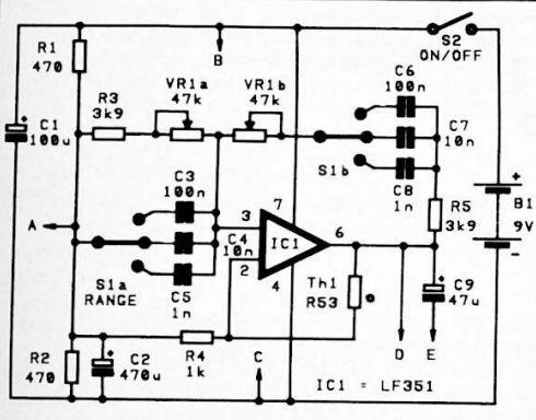
Fig. 1.3 The sinewave generator circuit
Circuit Operation
Figure 1.3 shows the circuit diagram for the sinewave generator section of the unit. The squarewave signal is produced from the sinewave signal using a simple converter circuit which appears in Figure 1.4. This second diagram also includes the output attenuator circuit.
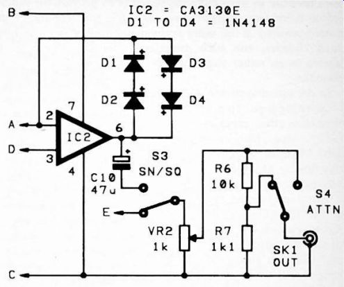
Fig. 1.4 The "squarer" and attenuator circuit
The sinewave generator circuit follows the basic configuration of Figure 1.2 quite closely, but to permit operation with a single 9 volt battery (rather than the dual supplies required by standard operational amplifier configurations) R1, R2, and C2 are used to provide a centre tap on the supply lines. This is used for biasing purposes. Th1 is the stabilizing thermistor.
Three ranges are provided by having three sets of capacitors in the Wien network, with S1 being used to select the required If desired, a four way switch plus an extra pair of set.
capacitors could be used to extend the coverage up to about 200kHz. The two extra capacitors would need to have a value of 100-p in theory. However, due to stray circuit capacitances a value of 82-p might offer better accuracy. A twin gang variable resistor (VR1) enables the output frequency to be continuously varied over the quoted ranges. It would be quite possible to have switched resistors to provide the ranges and a twin gang variable capacitor for fine tuning. The present method is the more popular one though, as it is very much cheaper, and each range is covered over about 270 degrees or so rather than the 180 degree travel of a variable capacitor.
In the squaring circuit IC2 operates as a voltage comparator.
Its inverting input (pin 2) is biased to the central bias voltage, while the other input is fed with the sinewave signal. On positive input half cycles the output of IC2 switches fully high, while on negative going input half cycles it switches fully low. Although I stated above that IC2's output goes fully positive and negative, this is not quite true. It tries to do so, but it is clamped at about plus and minus 1.3 to 1.4 volts by the four diodes at its output. This has two beneficial effects, one of which is to give an improved wave shape on the squarewave output. The other is to give a peak to peak output level that is a close match for the sinewave signal instead of being several times greater.
S3 is used to select the sinewave or squarewave signal, as required, and couple it through to the attenuator section of the unit. VR2 is the variable attenuator, while R6, R7, and S4 form the switched - 20dB attenuator. If a - 40dB attenuator is preferred (i.e. a one hundred fold decrease in the output level), simply change the value of R7 to 100 ohms.
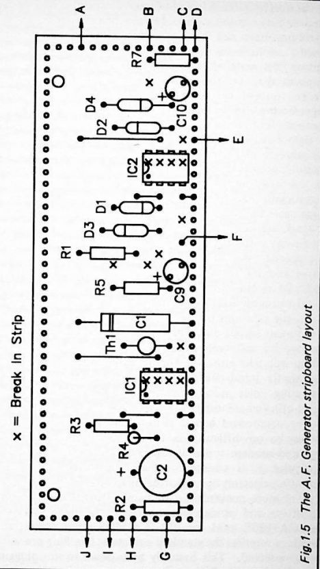
Fig. 1.5
The current consumption of the circuit is in the region of 15 to 16 milliamps, which is a little high to permit economic operation on a small 9 volt battery. A larger type such as six HP7 size cells in a plastic holder is a better choice.
Construction Details of the stripboard layout for the audio signal generator project are shown in Figure 1.5. This requires a 0.1 inch pitch stripboard having 42 holes by 14 copper strips. Stripboard is not sold in this size, and a larger piece must be trimmed down to the correct size. A board of these dimensions is most easily produced by cutting a piece 14 strips wide from a standard 5 inch long board, and then trimming it down to the appropriate length. A hacksaw or junior hacksaw are both suitable for cutting this material. Do not try cutting between rows of strips as they are too close together for this to give good results. Instead, cut through rows of holes. This leaves sawn edges having a rather rough finish, but they are easily filed to a smooth finish using a small to medium sized flat file.
Before fitting any of the components onto the board it is advisable to make the breaks in the copper strips, being very careful not to get any out of position. In fact it is easier to get the breaks in the correct places if they are made after the components have been fitted onto the board. However, in some cases the soldered joints will tend to spread over the area of track that must be broken, making it difficult to complete the breaks without damaging the soldered connections. There is a special track cutting tool available, but a hand-held drill bit of about 4 millimeters in diameter will do the job quite well. Be careful not to cut too deeply into the board, as this could seriously weaken it. As with the other projects in this guide, the positions of the breaks are marked by "X"s on the component layout diagram. At this stage you should also drill the two 3.2 millimeter diameter mounting holes for the board.
These will take either M3 or 6BA mounting bolts. You can use plastic stand-offs if preferred, but the diameter of the mounting holes must then be chosen to suit the particular stand-offs you are using.
The component layout is not unduly crowded, and there should be no difficulty in fitting the components in place provided modern types of reasonably small size are used. In particular, it is advisable to use miniature printed circuit mounting electrolytic capacitors, apart from C1 where an axial type is more convenient. Be careful to get the electrolytic capacitors and semiconductors fitted the right way round.
The CA3130E used for IC2 is a MOS input device, and it therefore requires the standard anti-static handling precautions to be observed. This basically boils down to not plugging it into circuit until all the other components have been fitted and all the wiring-up has been completed. Until that time it should be left in the protective packaging (such as a plastic tube or conductive foam) in which it should have been supplied. Use a holder for this component, and handle the device as little as possible when fitting it into the board. Although the LF351 used for IC1 is not a MOS input integrated circuit I would still recommend the use of a holder for this component (or any other DIL integrated circuit come to that).
The thermistor (Th1) with its glass encapsulation should obviously be treated with reasonable respect. This component seems to be available as either an "RA53" or an "R53". As far as I can ascertain there is no difference between these two components, and either should work well in this circuit.
No other types are likely to give good results though.
There are a few link wires needed, and trimmings from resistor and capacitor leadout wires will probably be sufficient for these. If not. some 22 or 24 s.w.g. tinned copper wire will be required. These link wires must be quite taut so that there is no risk of them short circuiting to any of the component leadout wires. Either this, or they must be fitted with PVC sleeving to insulate them. At this stage only fit printed circuit pins to the board at the points where connections to off- board components will eventually be made, 1 millimeter diameter pins are required for normal 0.1 inch pitch stripboard.
It would probably be possible to fit this unit into quite a small case if required, but it will probably be easier to use if one having dimensions of about 150 by 100 by 50 millimeters or more is used. This avoids crowding of the controls on the front panel, and permits VR1 to be fitted with a fairly large calibrated scale if desired. A large scale is advantageous as it enables the output frequency to be set with greater accuracy.
The exact layout of the front panel components is not critical, but the hard-wiring will be easier if the layout does not necessitate a large number of long trailing wires and crossed-over wires. I used a 3.5 millimeter jack socket for SK1, but any two way audio type should be suitable. Note that most 3.5 millimeter jack sockets are fitted with a break contact which is unused in this application. Hence one tag of this socket is left unconnected.
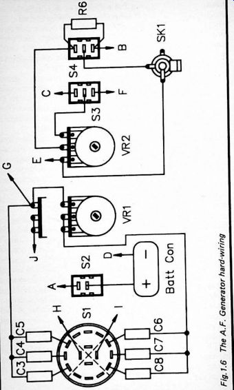
Fig. 1.6
Figure 1.6 gives details of the hard-wiring, and this diagram must be used in conjunction with Figure 1.5 (e.g. point "A" in Figure 1.5 connects to point "A" in Figure 1.6). This wiring is largely straightforward, but some of the components are mounted on the switches, and the wiring will almost certainly be easier if these are added first. If the unit is powered from six HP7 size cells in a plastic holder, the connections to the holder are made via a standard PP3 type battery connector.
The capacitors in the Wien network (C3 to C8) are specified as having a tolerance of 5% or better in the components list.
A fairly close tolerance for these components is important for two reasons. The first of these is simply that large tolerances could result in the frequency coverages of the three ranges being well away from the required ones. This could leave gaps in the coverage of the unit. The second reason is that it is much easier to calibrate the frequency control if a single scale is used for all three ranges. A single scale will only give good accuracy on all three ranges if the sets of capacitors have a close tolerance, so that there is an accurate ratio of ten to one between one range and the next. I would regard 5% as the minimum acceptable tolerance, and 1% or 2% is better.
The two attenuator resistors are specified as 2% types, and this is to ensure a reasonably accurate reduction by 20dB when the attenuated output is selected. However, you should bear in mind that loading on the output of the unit will have some effect on the output level, especially when the unit is set for anything other than maximum output. The exact effect of output loading depends on the input impedance of the circuit driven by the unit. With a high input impedance of about 100k or more there is unlikely to be any significant reduction in the output level. With a load impedance of a few tens of ohms or less the unit may well be overloaded and cease to function properly at all. Where precise output levels are required it is essential to monitor the output level using an AC millivoltmeter or an oscilloscope, rather than relying on any calibration on the attenuator controls.
Components for Figures 1.3 and 1.4
Resistors (all 0.25 watt 5% unless noted)
470 R1 470 R2 3k9 R3 1-k R4 3k9 R5 10k (2% tolerance)
1k1 (2% tolerance) R6 R7
Potentiometers
VR1
VR2
47k 1-in dual gang (see text)
1k 1- in
Capacitors
100u 10V axial elect 470u 10V radial elect 100 nF plastic foil 5% or better 10n plastic foil 5% or better In plastic foil 5% or better 100 nF plastic foil 5% or better 10n plastic foil 5% or better 1 n plastic foil 5% or better 41 p 16V radial elect 41 p 16V radial elect
C1 C2 C3 C4 C5 C6 C7 C8 C9 C10
Semiconductors
LF351 CA3130E 1N4148 1N4148
1N4148
1N4148
IC1 IC2
D1 D2 D3 D4
Miscellaneous
SK1 3.5mm jack socket 3 way 4 pole rotary (only two poles used)
SPST miniature toggle SPDT miniature toggle S1 S2 S3
S4 SPST miniature toggle 9 volt (e.g. 6 x HP7 cells in plastic holder)
R53 or RA53 thermistor B1 Th1
Case
0.1 inch matrix stripboard 14 strips by 42 holes
Two control knobs Two 8 pin DIL IC holders
Battery connector
Wire, solder. 6BA or M3 fixings, etc.
Testing and Calibration
In order to check the unit it is obviously necessary to have some means of monitoring of its output signal. Ideally an oscilloscope should be used, but an audio amplifier and a loudspeaker will suffice. Medium or high impedance headphones are also suitable, as is a crystal earphone. It is just a matter of checking that an output signal is present, that the attenuator controls enable the output level to be adjusted, and that the frequency controls provide coverage of the full audio range. Bear in mind that the sinewave output from the unit will be inaudible at the extremes of the frequency range. Accordingly, the fact that no output is audible at very high and very low frequencies does not necessarily mean that the unit is faulty. In all probability it is not. You can check that the unit is functioning at very low frequencies by switching to the squarewave mode. The harmonics on this signal should be clearly audible even if the fundamental frequency is not. A lack of any clearly audible output with the controls set for a low frequency sinewave, but a low frequency "buzzing" sound when the unit is set for square- wave operation, is a good indication that the unit is functioning correctly. If no output can be detected regardless of the control settings, or there is obvious distortion on the sinewave output, switch off at once and recheck all the wiring.
For the generator to be really useful it is essential for it to be fitted with an accurate frequency scale around VR1's control knob. If some form of frequency meter or an accurately calibrated oscilloscope is available there should be no difficulty in providing the unit with a suitable scale.
Without the aid of suitable test equipment things are very much more difficult. About the only other option is to use a musical instrument to provide a range of known frequencies.
The signal generator can then be tuned to the same pitches "by ear". This is a list of frequencies from middle A to the A one octave higher.
440Hz 466Hz 494Hz 523Hz 554Hz 587Hz 622Hz 659Hz 698Hz 740Hz 784Hz 831 Hz 880Hz
A A# B C C# D D# E F F# G G# A
In each case these frequencies have been rounded up or down to the nearest Hertz. At frequencies of a few hundred Hertz you are unlikely to be able to produce a scale that can be read to within 1Hz. In fact the calibration points will probably have to be quite well spread out. but this should still provide a frequency scale that is adequate for most audio testing. Although only a limited range of frequencies are covered by the notes given above, bear in mind that an increase by one octave represents a doubling of frequency, while a reduction by one octave represents a halving in frequency. The note of B is a useful one as it is very close to 500Hz. Therefore, the Bs one octave above and below this are at frequencies close to 1kHz and 250Hz respectively.
Obviously a musical instrument which has a wide compass will provide a good range of calibration frequencies.
A point to note is that the scaling is far from linear. The scale is well spread out at the low frequency end of the range but is much more cramped at the high frequency end. It is possible to obtain something close to linear scaling by using a potentiometer having an anti-log law for VR1. However, a suitable component is likely to prove impossible to obtain. An alternative is to use a log law potentiometer, but reverse connected (i.e. swop over the two track connections for each gang). The only disadvantage of this system is that the scale is reverse reading, with clockwise adjustment of VR1 producing a decrease in frequency.
An audio signal generator can be used in isolation as a signal injector, but it is normally operated in conjunction with other test equipment such as an audio millivoltmeter. We will consider the use of an audio signal generator for such tests as frequency response and voltage gain testing later in this Section.
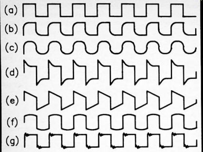
Fig. 1.7 Squarewave testing waveforms
Square wave Testing
If you have access to an oscilloscope, this can reveal some basic information about the phase and frequency response of a circuit when used in conjunction with the squarewave output of the signal generator. The basic technique is to simply inject the squarewave signal into the circuit under test, choosing sensible amplitude and frequency settings, and to then view the resultant output waveform. If the signal undergoes no significant changes in phase or frequency content it should emerge unaltered, as in Figure 1.7(a).
With an ideal squarewave signal the waveform jumps instantly from one level to the other. No practical circuit can produce such a waveform, but with most audio squarewave generators the rise and fall times of the circuit are no more than about a microsecond. Any lack of frequency response in a circuit that passes a squarewave will result in an increase in the rise and fall times. Figure 1.7(b) shows the effect of both inadequate high frequency bandwidth and phase shifting (which usually accompany any high frequency roll-off). Figure 1.7(c), shows the waveform obtained with the high frequency roll-off but no attendant phase shifting.
Inadequate low frequency response results in the horizontal parts of the waveform sloping diagonally, and a rise in the frequency response above the squarewave frequency has a similar effect. Figure 1.7(d) shows the effect of this rising response, while Figure 1.7(e) shows the effect of low frequency roll-off. A rising low frequency response gives rounded tops and bottoms to the waveform, as in Figure 1.7(f).
Instability can manifest itself in a number of similar ways.
In a mild case there would be slight over-shoot on the leading and trailing edges of each cycle. In a more extreme case there would be "ringing", as in Figure 1.7(g).
These waveforms are ail dependent on a suitable input frequency being chosen. When testing tone controls of an amplifier for example, a middle audio frequency of about 800Hz to 1kHz would be selected. Adjusting the tone controls should then have the appropriate effect on the output waveform. Obviously this system does not provide precise information about phase and frequency responses, but it is useful for giving certain types of equipment a quick check.
Test Bench Amplifier
A test bench amplifier is one of those simple little gadgets that no one involved with audio equipment can afford to be without. It can be used for checking signal sources such as microphones, tuners, tape decks, etc., as well as operating as a signal tracer when checking faulty equipment. Basically a unit of this type is just an audio power amplifier having reasonably good sensitivity and a high input impedance. This permits low output devices such as microphones to be checked, and ensures minimal loading on any audio circuit being tested. High output power is not usually of prime importance, and a small battery powered device is adequate for most purposes.
This bench amplifier requires an input of only about 10 millivolts RMS for maximum output, but it will produce a clearly audible output from inputs of below 1 millivolt RMS The output power is less than 100 milliwatts into the built-in high impedance loudspeaker, but this provides reasonable volume (aided by the fact that high impedance loudspeakers tend to be somewhat more efficient than lower impedance types of a similar size). The input impedance depends on the setting of the volume control, but is always quite high at around 200 to 500 kilohms.
Amplifier Circuit
The full circuit diagram for the Test Bench Amplifier appears in Figure 1.8. It is a two stage affair having TR1 as the preamplifier and IC1 as the class B power amplifier.
The preamplifier is a common emitter amplifier. A stage of this type would normally be expected to have a very high level of voltage gain (often in excess of 40dB). In this case the voltage gain is quite modest at about 20dB (ten times) due to the local negative feedback provided by unbypassed emitter resistor R3. Slightly higher voltage gain would be quite useful, but a realistic figure for the overall voltage gain must be selected. A very high level of voltage gain runs the risk of instability due to stray feedback. There are also problems with stray pick-up of electrical noise such as mains "hum" when the input of the unit is left open circuit, or when it is fed from a high source impedance. The level of gain obtained with the specified value for R3 provides useful results without too much risk of problems with instability or excessive stray pick-up.
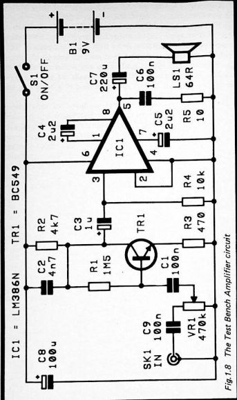
Fig. 1.8
A useful byproduct of the negative feedback provided by R3 is that it boosts the input impedance of TR1, thus avoiding the need for a separate input buffer stage. The input impedance is shunted somewhat by the volume control, VR1. This must be included at the input of the circuit as the input level could be quite high in some instances. Although there are advantages in having the volume control between the preamplifier and power amplifier stages, this is not an acceptable way of arranging things in this application, since there would be a strong likelihood of the input stage being severely overloaded on many occasions. C2 provides a small amount of high frequency roll-off, and this aids good stability.
Capacitor C9 was not included in the original design, but was added to the final version. Without this component there are two problems that can occur. The first of these is that there may be a d.c. component on the input signal. Without C9 included in the circuit this d.c. signal will be present across VR1's track and will tend to make operation of this control rather "noisy". It could even result in the biasing of the circuit being temporarily shifted to unusable levels each time VR1 was adjusted. The second reason is simply that the resistance of VR1 could shunt bias components in the circuit under test. This could cause a malfunction in the circuit under investigation each time the amplifier was connected to it. This could obviously cause confusing and misleading results.
The audio power amplifier device is the LM386N, which is a fairly standard low power type. Using a 9 volt supply it is capable of delivering a few hundred milliwatts RMS into an 8 ohm impedance loudspeaker. The use of a high impedance loudspeaker and the lower output power that this provides is probably advisable in this case though. Using a low impedance loudspeaker the component layout and wiring needs to be carefully designed and implemented if problems with earth loops are to be avoided. Construction is far less critical using a high impedance loudspeaker, the battery consumption is much lower, and the volume is still quite adequate.
C6 and R5 form a "Zobel" network at the output, and this helps to avoid problems with instability caused by anomalies in the loudspeaker's impedance characteristic. C5 is a decoupling capacitor, and C4 is part of the negative feedback network which sets the voltage gain of 1C1. The other feedback components are included within IC1. The typical closed loop voltage gain is 26dB (twenty times).
The quiescent current consumption of the circuit is only about 5 milliamps, but it is several times higher than this on volume peaks. A PP3 size 9 volt battery is adequate as the power source, but if the unit is likely to receive a great deal of use it is probably better to use a higher capacity battery.
Six HP7 size cells in a plastic holder should suffice. The connection to this type of holder is made via a standard PP3 style battery clip.
Construction
The stripboard layout for the Test Bench Amplifier project is shown in Figure 1.9. It requires a board having 32 holes by 16 copper strips.
I will not give a detailed description of building the board as the method used is much the same as for the Audio Signal Generator project described earlier in this Section. IC1 is not a MOS input device, but I would still recommend the use of a holder for this component.
It should be possible to fit the unit into any medium sized plastic box (i.e. one about 150 by 100 by 50 millimeters). A loudspeaker grille is required, and my preferred method of producing one of these is to simply drill a matrix of small holes (say about 5 millimeters in diameter). Take due care when drilling the holes as it is very easy to get some of them just slightly out of position, and this can give the finished unit a rather scrappy appearance. An alternative method is to make a large cutout in the front panel and to then glue some loudspeaker material in place behind this.
Plastic grille material is also suitable, but seems to be difficult to obtain these days.
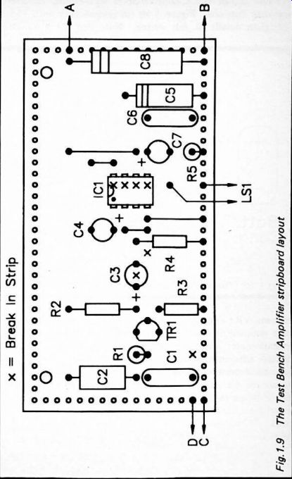
Fig. 1.9
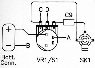
Fig. 1.10 The wiring diagram for the Test Bench Amplifier.
Built-in mounting brackets are a standard feature on medium and large loudspeakers, but seem to be absent from virtually all miniature types. This leaves little option but to glue the loudspeaker in position behind the grille. Any good quality general purpose adhesive should be suitable. I mostly use a quick setting epoxy type for this sort of thing. Be careful to only apply the adhesive to the front of the loudspeaker's outer rim, and avoid getting any onto the diaphragm.
There is not much point-to-point style wiring needed to complete the unit. Figure 1.10 (in conjunction with Figure 1.9) gives details of this wiring. Note that C9 is mounted between VR1 and SKI, and is not fitted on the circuit board.
It is assumed in Figure 1.10 that VR1 and S1 are a switched potentiometer which provides a combined volume and on/off switch. Obviously a separate switch and potentiometer could be used if preferred. Similarly, SK1 is a 3.5 millimeter jack socket on the prototype, but any two way audio connector should be perfectly suitable. Provided the wiring is kept quite short there should be no need to bother with any screened leads. Try to keep the leads to L S1 well away from any of the input wiring.
Components for Figure 1.8
Resistors (all 0.25 watt 5%)
R1 1M5 R2 4k7 470 R3 10k R4 R5 10
Potentiometer
VR1 470k log with switch ( S1)
Capacitors:
100n polyester 4n7 polystyrene
1-uF 63V radial elect
2u2 63V radial elect
2p2 63V axial elect
100 nF polyester
200u 10V radial elect
100u 10V axial elect
100n polyester
C1 C2 C3 C4 C5 C6 C7 C8 C9
Semiconductors:
LM386N BC549
IC1 TR1
Miscellaneous:
Part of VR1 3.5mm jack socket 9 volt (e.g. 6 x HP7 size cells in holder)
66mm diameter. 64R impedance
S1 SK1 B1 LS1
Case about 150 x 100 x 50mm 0.1 inch pitch stripboard 32 holes by 16 copper strips Battery connector 8 pin DIL holder
Control knob
Fixings, wire, solder, etc.
In Use
You could use ordinary multimeter type test prods with a unit of this kind, but this is not a particularly good way of doing things. The problem is that there tends to be strong pick-up of electrical noise by the long and unscreened (non-earthy) input lead. A better method for an application of this type is to use a screened lead to connect the test prods to SK1. On the face of it this leaves the user with two test prods very close together, and probably unusable in many situations. In practice the earthy test prod is usually connected to the outer braiding of the screened cable via a fairly long insulated lead (ordinary multi-stand connecting wire is suitable for this). This gives good separation of the test prods, but keeps the non-earthy lead screened as far as possible. Figure 1.11 illustrates this general scheme of things.
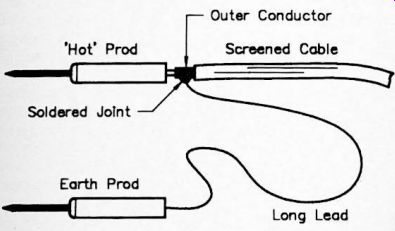
Fig. 1.11 The basic arrangement used for screened test leads.
Make sure you connect the screened cable to the 3.5 millimeter jack plug correctly. The small tag towards the front of the plug is the non-earthy ("hot") one, and the larger tag (which is usually part of the cable grip) is the earth tag.
In use it is just a matter of switching on using S1, connecting the input signal to the unit, and adjusting VR1 for a suitable volume level. If you use the unit as a signal tracer it is important to ensure that the unit under test is fed with a suitable test signal for you to trace! The normal input signal of the equipment is probably the best one to use wherever possible, as this will obviously be at the correct amplitude. If this is not practical for some reason, then a unit such as the Audio Signal Generator project described earlier should be able to provide a suitable test signal. If you use a signal generator as the signal source, set it to the sinewave mode.
Any distortion will be readily detectable by ear using a sine-wave test signal.
There are several techniques for fault-finding with the aid of a signal tracer, although these are really just variations on the fundamental method of operation. It is basically a matter of checking for a suitable signal level at various points in the circuit under test. In some cases it is not a lack of signal that is the problem, but severe distortion. In this eventuality you check for a distorted signal rather than a lack of signal level.
What you are searching for are two points in the circuit that are close together; one which provides a suitable signal and one that does not. The fault is then at or very close to the point in the circuit where there is a lack of signal or excessive distortion. It is important to realize that signal tracing techniques do not always narrow down the fault to a specific component. In most cases only the general area of the fault is identified. Some further testing, such as voltage and component checks, will then usually identify exactly which component or components are faulty.
As an example of how signal tracing is undertaken, assume that the test bench amplifier is to be used for signal tracing on another test bench amplifier unit of the same design. Some form of audio signal would be connected to the input of the amplifier under test, and this could be (say) the audio output from the earphone socket of a transistor radio, or the output of an audio signal generator. The first check could be at SKI to test that the input signal was getting through to the socket correctly. A lot of faults with audio equipment actually turns out to be problems with faulty plugs and leads! The next test points could be at the top end of VR1's track and at its wiper.
The signal should be much the same at the top of VR1's track as it was at SK1, but at the wiper it should be possible to vary the signal level by altering VR1's setting. The next test would be at the base of TR1. where the signal level should be much the same as at die wiper of VR1. Bear in mind that at any point in the circuit after the volume control, the signal level will vary according to the setting of the volume control.
TR1's collector is the next test point, and as TR1 provides about 20dB of voltage gain, the signal level here should be noticeably higher than that at TR1's base. You cannot make precise gain measurements using a test bench amplifier, but with experience you can learn to gauge voltage gains reasonably accurately.
It can sometimes be helpful to test for signals at places other than in the main signal path. In this case there is no bypass capacitor across R3, and the signal level here should be very much the same as that at the base of TR1. With a lot of common emitter amplifiers that have an emitter resistor it is bypassed by a capacitor, and there should then be no significant signal level at the emitter of the transistor. If a significant signal level is detected, this would suggest that the bypass capacitor is faulty. In a similar vein, it can sometimes be helpful to test for a signal on the non-earthy supply rail.
This often has a supply decoupling capacitor (like C8), and in a fairly complex audio circuit there will normally be one or more R - C filter stages in the supply to the early stages of the circuit. There would normally be little or no detectable signal on the supply rails, and the presence of a significant signal level would strongly suggest that one of the supply decoupling capacitors was faulty.
For the sake of this example we will assume that the signal is found to be present and correct at the collector of TR1, but is absent at pin 3 of IC1. The fault obviously lies in the circuitry around C3, but it is not necessarily C3 that is faulty.
As the signal is present at TR1's collector it would seem unlikely that the fault lies on this side of C3. Although not necessarily due to C3 being faulty, with further thought it would seem quite likely that this component is indeed the cause of the problem. However, R4 having gone closed circuit could give the same result. On the other hand, this would place strong loading on the output of TR1, and would almost certainly produce quite noticeable distortion on the output from TR1 except at very low signal levels. A fault at the input of IC1 could have a similar effect. In the absence of any strong distortion on the output from TR1 it would seem likely that C3 is the faulty component, or that it is not connected into circuit properly. A few continuity checks, component checks, or component substitutions should sort out the precise nature of the problem.
Audio Millivoltmeter
A test bench amplifier is all that is needed for much audio testing, but its inability to measure precise signal levels is a severe handicap for many types of checking. For tests such as accurate gain measurements and frequency response testing it is essential to have a device that can at least accurately measure relative signal levels. Ideally it should also be able to measure absolute AC voltages with reasonable accuracy. One method of measuring signal levels is to use an oscilloscope.
Although these instruments often seem to be regarded as only for viewing waveforms, they are in fact used just as much for voltage and time measurements as for viewing wave shapes.
Despite price drops in "real terms" over the years, an oscilloscope is still a fairly expensive item of equipment, and one which a lot of amateur electronics enthusiasts consider (quite understandably) to be far too expensive to be worth buying.
A cheaper alternative for audio signal measurements is an AC millivoltmeter. This is similar to an ordinary multimeter switched to an AC voltage range. However, whereas most multimeters have a full scale value of a few volts on their most sensitive AC voltage range, an AC millivoltmeter at its most sensitive might require only a millivolt or less for lull scale deflection of the meter. Also, it has a relatively high input impedance so that readings are not affected by substantial loading on the circuit under test. Another difference is that many multimeters switched to an AC voltage range offer a bandwidth that is somewhat less than the full audio range.
Digital instruments tend to be the worst offenders in this- respect, and often have an upper limit to their frequency responses of only a few hundred hertz. Most AC millivolt- meters have upper frequency responses that extend well beyond the upper limit of the audio range, often to frequencies of a few hundred kilohertz or more.
This is a relatively simple instrument that offers three measuring ranges with full scale values of 10 millivolts RMS, 100 millivolts RMS, and 1 volt RMS The input impedance is over 1 megohm, although the unavoidable input capacitance reduces the input impedance significantly at high frequencies. On all three ranges the upper limit of the frequency response is beyond the 20kHz upper limit of the audio frequency range, but due to the simplicity of the design the response does not extend far beyond 20kHz. This offers adequate performance for most audio testing, while not providing such high levels of sensitivity, bandwidth, and input impedance that the unit becomes excessively difficult to build and use.
Linearity
On the face of it there is no difficulty in producing an AC millivoltmeter that will provide accurate results. All that is needed is an amplifier driving a meter via a rectifier circuit.
In reality a circuit of this type is unlikely to give really good results. The problem is the severe non-linearity of semiconductor diodes. Silicon types are amongst the worst offenders, and these require a forward voltage of around 0.5 to 0.6 volts before they will start to conduct significantly.
There are diodes which perform better in this respect, including the old germanium and gold bonded types (the latter being a popular choice for AC meter circuits).
Even using these lower voltage drop diodes, at low input voltages there is usually quite significant non-linearity. In analog multimeters the normal way around the problem is to use a separate scale for the lower AC voltage ranges, with the scale being adjusted to match the non-linearity of the diodes. This is not a very convenient way of tackling the problem in a home constructor project where accurately calibrating the finished unit could prove to be very difficult.
Ideally what is needed is a circuit that provides linear scaling so that the original scale of the meter can be utilized.
This can be achieved by using negative feedback to compensate for the non-linearity of the diodes. Even using diodes with a large forward voltage drop it is possible to obtain really good linearity if sufficient feedback is used (although results will always be that much better using low voltage drop diodes). Figure 1.12 shows the standard method of using negative feedback to overcome the non-linearity of semiconductor diodes.
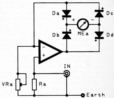
Fig. 1.12 Basic full wave precision rectifier circuit.
The circuit is basically a standard operational amplifier non-inverting mode circuit. However, rather than driving the rectifier and meter from the output of the amplifier and the 0 volt earth rail, they are included as part of the negative feedback circuit. With insufficient output voltage to drive the diodes into conduction, there is no significant feedback and the amplifier exhibits its full open loop voltage gain. Thus, only a very small input voltage is needed in order to produce a large output voltage. What happens in practice is that very early in each input half cycle the output voltage becomes sufficiently large to bring the diodes into conduction. Strong negative feedback is then applied to the amplifier, which consequently has a much lower closed loop voltage gain. A sinewave input signal, as in Figure 1.13(a), therefore provides a rectified output signal more like that of Figure 1.13(b).
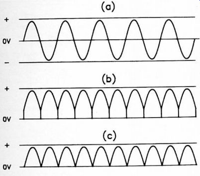
Fig. 1.13 Precision rectifier waveforms
Due to the voltage drops through the diodes, this gives a properly rectified signal across the meter, as in Figure 1.13(c). The feedback is effectively boosting the output voltage by an amount which is equal to the voltage drop through the diodes, and which consequently compensates for this voltage loss.
The Circuit
Figure 1.14 shows the full circuit diagram of the AC millivolt- meter project, and as will be apparent from this, the unit is based on just a single integrated circuit. This is the CA3130E, which is a high performance operational amplifier that can provide excellent bandwidth, a very high input impedance, and will operate with a single supply rail. The use of other operational amplifiers in this circuit is not recommended, and would almost certainly result in grossly inadequate performance. In fact most other types will not operate with a single supply rail, and are totally unusable in this circuit.
This circuit uses a form of rectifier that is somewhat simplified in comparison to the configuration of Figure 1.12.
It differs from this mainly in that it is based on a half wave rectifier, not a full wave type. D1 is included in the feedback circuit in order to compensate for the voltage drop through D2, and the method of operation is essentially the same as that of the full wave circuit. Both diodes are germanium types so that IC1 has as little work to do as possible. This helps to maintain good performance at high frequencies.
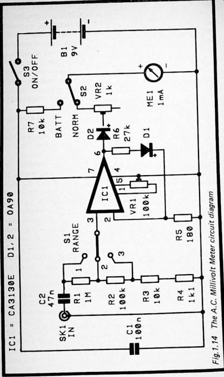
Fig. 1.14
VR2 enables the sensitivity of the unit to be varied so that it can be accurately calibrated. In the "BATT" position of S2 the meter is used to monitor the battery voltage, and ME1 then has a full scale reading of approximately 10 volts. A reading of less than about 7.5 volts indicates that a new battery is required. VR1 is an offset null control. This is used to trim out any offset voltages that might otherwise result in the meter reading above zero with no input signal.
The input signal is taken via d.c. blocking capacitor C2 to a three step attenuator. This provides attenuation levels of 0 dB. 20 dB, and 40 dB. Together with the unit's basic full scale sensitivity of 10 millivolts RMS, this gives full scale sensitivities of 10 millivolts r.m.s on range 1. 100 millivolts RMS on range 2, and 1 volt RMS on range 3. As the attenuator is in a high impedance part of the circuit there is a risk of it introducing anomalies in the frequency response of the unit. In practice this does not seem to be a major problem, especially as the unit is not intended for operation at high frequencies beyond about 20kHz anyway.
IC1 is not an internally compensated device. Normally a small capacitor of around 2pF to 30pF would be connected between pins 1 and 8 in order to ensure good stability. With this circuit, where IC1 is used at a fairly high closed loop voltage gain, this capacitor does not seem to be necessary. It is advisable not to include a compensation capacitor unless it is really necessary as it will reduce the high frequency performance of the circuit. If any problems with instability should be experienced, connecting a compensation capacitor of around 1pF or 2pF in value between pins 1 and 8 of IC1 might effect a cure.
The current consumption of the circuit is quite low at only about 2 milliamps. A small 9 volt battery such as a PP3 or equivalent is therefore perfectly adequate as the power source.
Construction
Details of the stripboard for the AC millivolt meter are provided in Figure 1.15. This requires a board having 17 holes by 19 copper strips. Construction of the board is quite straightforward, but note that IC1 is a MOS device which consequently requires the usual anti-static handling precautions to be taken. Do not overlook the four link wires. If the preset resistors are to fit into the layout properly they must be miniature horizontal mounting types. D1 and D2 are germanium diodes, and as such they are more vulnerable to heat damage than are the more common silicon types. It should not be necessary to use a heat shunt when soldering these components into place, but do not apply the iron to each of these joints for any longer than is absolutely necessary.
The hard-wiring is shown in Figure 1.16. It is important that the input wiring is kept as short as possible to minimize any risk of instability or excessive stray pick up in this wiring.
It is therefore important to have SK1 mounted near to S1, and to have the circuit board mounted close to S1 as well.
Also try to keep the wiring to S2 and ME1 reasonably short, and as far as possible, well separated from the input wiring. I would strongly urge the use of an all metal case for this project. If this is earthed to the negative supply rail it will tend to shield the sensitive input wiring from any electrical noise in the vicinity of the unit, if an ordinary 3.5 millimeter jack socket is used for SK1, this will provide the earth connection to the case. If an insulated socket of some kind is used for SK1, then a solder-tag on the case can be used to provide an earth connection point.
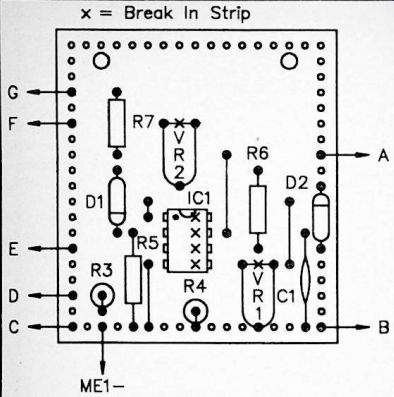
Fig. 1.15-- The millivoltmeter stripboard layout.
S1 is a standard 3 way 4 pole rotary switch, but in this application only one pole is required. This leaves nine of its tags unused. R1 and R2 are mounted on S1, and C2 is mounted between S1 and SK1. This helps to minimize the amount of input wiring and aids good stability. It is obviously helpful if C2 is a type which has fairly long leadout wires, rather than one which has very short leads for printed circuit mounting.
However, if necessary it should not be too hard to solder short extension leads to C2. Note that the attenuator resistors (R1 to R4) should have a tolerance of 2% (and preferably 1%) in order to ensure good accuracy on all three ranges. Avoid over-heating them when soldering them in place, as this could impair their accuracy.
One slightly awkward aspect of construction is mounting the meter. These mostly require quite a large circular cutout, usually about 38 millimeters in diameter. Without access to sophisticated cutting equipment, a fret or coping saw represents about the easiest method of making this cutout.
A miniature round tile can also be used, but will make somewhat tougher going of the task. Either way, it is probably best to cut just inside the line marking the perimeter of the cutout. Then use a large round file to enlarge the cutout to precisely the required size.
Any recalibration of the meter is not really necessary. The 0-1 scale is correct for the 1 volt range, and on the other two ranges it is not difficult to convert meter readings to the millivolt readings they represent. If you do decide to add to the meter's scale, proceed with great caution. It is quite easy to take off the front panel of most meters, unscrew the scale plate, add some figures using rub-on transfers, and then reassemble everything. On the other hand, it is even easier to damage the delicate meter mechanism while doing this. You have been warned!
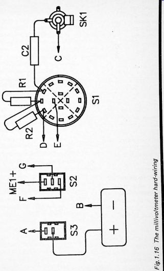
Fig. 1.16
Components for Figure 1.14
Resistors (all 0.25 watt 5% unless noted)
1M 2% 100k 2% 10k 2% 1k1 2%
R1 R2 R3 R4 R5 180 R6 27k R7 10k 2%
Potentiometers
VR1 VR2
100k sub-min hor preset
1k sub-min hor preset
Capacitors
100 nF ceramic 47n polyester C1 C2
Semiconductors
CA3130E OA90 OA90
IC1 D1 D2
Miscellaneous
ME1 1mA moving coil panel meter 3 way 4 pole rotary (only 1 pole used)
SPDT miniature toggle
SPST miniature toggle 9 volt (PP3 size) 3.5mm jack socket
S1 S2 S3 B1 SK1
Metal instrument case
Battery connector
Control knob 0.1 inch pitch stripboard 17 holes by 19 strips Pins, fixings, wire, solder, etc.
Calibration
Obviously the unit must be accurately calibrated if it is to be used for absolute measurements. For relative tests such as frequency response measurements a lack of calibration accuracy will not hinder results. In order to calibrate the unit you will require a sinewave signal source (such as the audio signal generator unit described previously) and an AC voltmeter, oscilloscope, or millivoltmeter. It is unlikely that many constructors of this project will have access to either an oscilloscope or AC millivoltmeter, but presumably anyone building the unit will have a multimeter in their possession.
Digital multimeters probably offer the best alternative to an AC voltmeter. They normally have a low AC voltage range (usually 1.999 volts full scale) which can be used to accurately set the output of the signal generator at 1 volt RMS. You need to be careful with the choice of calibration frequency though. Most digital multimeters are only accurate at frequencies of up to a few hundred hertz. Setting the signal generator for an output frequency of about 100Hz to 200Hz should give good results. Most analog multimeters have a low AC voltage range, but it may not be low enough to permit a level of one volt RMS to be set really accurately. This obviously depends on the quality of the instrument concerned. Many will allow this voltage level to be set with good accuracy.
Having set the signal generator to a suitable audio frequency, and having set its output level as accurately as possible to 1 volt r.m.s you are ready to commence calibration. Start with both presets at roughly mid settings. First offset null control VR1 must be given the correct setting. In order to do this, first switch the unit to the 10 millivolt range and short circuit die input (to eliminate any stray pick up). You should find that by adjusting VRI you can obtain a deflection of the meter which can be varied from zero to (probably) more than full scale deflection of ME1. Back-off VR1 just far enough to zero the meter. Turning it back too far will impair the accuracy of the unit at low readings, and so it is very important not to back it off excessively.
Next switch the millivoltmeter to its 1 volt range and feed it with the output of the signal generator. Then simply adjust VR2 for precisely full scale deflection on MF1. This completes the calibration process, and the unit is then ready for use.
In Use
Ordinary test prods are of little use with an instrument of this type. You should make up a set of test leads of the type described previously in the section of this Section dealing with the test bench amplifier. Ready-made test leads of this type can be obtained, and they are usually fitted with BNC connectors. If you use test leads of this type, obviously SK1 must be a BNC socket, or the plug on the lest leads must be removed and replaced with a 3.5 millimeter jack plug (or a plug to suit whatever type of socket you have used for SK1). Ready-made test leads are mostly excellent, but they are really intended for use with oscilloscopes. They are suitable for operation at frequencies of typically up to about 50MHz, and as a result of this they are rather over-specified for the present application, and are quite expensive.
An AC millivoltmeter can be used on its own for such things as checking the output levels from microphones, tuners, cassette decks, etc., or measuring noise levels. It is more usual for an instrument of this type to be used in conjunction with an audio signal generator though. As a simple example, assume that you wish to check the voltage gain of a preamplifier. The signal generator would be set to a suitable frequency (most audio testing is carried out at a middle audio frequency of around 800Hz to 1kHz), and then with the aid ol the AC millivoltmeter it would be set for an appropriate output level. It is important to choose a suitable input level. An excessive level could produce an output signal that is too strong to be measured by the millivoltmeter, although it might then be possible to measure it using a multimeter switched to a low AC voltage range. It is probably best to avoid high output levels though. These can cause clipping of the output signal which would give misleading readings. A low input level will probably give quite good results, but in an extreme case the noise level of the circuit under test could compromise the accuracy of readings. If you know that the preamplifier should have a gain of (say) 46dB (about 200 times), then an input level of 2 millivolt would seem about right. This gives an expected output voltage of 400 millivolts (2 millivolts x 200 = 400 millivolts). This is well within the maximum reading of the millivoltmeter, and is unlikely to overload the preamplifier.
Having set a suitable input level, it is then just a matter of measuring the output level. The voltage gain is equal to the output voltage divided by the input voltage. For instance, if the output level was measured at 575 millivolts, the voltage gain would be 287.5 times (575/2 = 287.5). If gain measured in decibels is required, decibel scales could be added to the meter's scale plate. This would be difficult to achieve in practice though. It is more realistic to make linear gain measurements and then convert them to decibels when necessary.
Frequency response testing is carried out in a similar fashion, but gain tests must be made at a range of frequencies.
The results would then normally be plotted on a graph. Just how many test frequencies should be used depends on the frequency range involved and the attenuation rate of the filtering. A large number of test frequencies will ensure accurate results with no slight peaks or troughs in the response passing unnoticed. However, for much frequency response testing no more than a dozen measurements are needed in order to obtain an accurate representation of the test circuit's frequency response.