What should undoubtedly be the first piece of electronic test equipment purchased by any electronics enthusiast is a multimeter. However, there are many electrical quantities that can be measured but which are not covered by most multimeters.
A multimeter is an invaluable piece of test equipment, but it is not a universal panacea for all electronic ills. The audio millivoltmeter described in the previous Section is an example of a form of metering that an ordinary multimeter can not handle properly. In this Section we will look at a few other electronic test meters which fill in the gaps left by most multimeters.
Voltage Loading
The first project in this Section is a high resistance voltmeter (also known as a high impedance voltmeter). This is a voltmeter which has a very high input impedance so that it does not tap off a significant amount of current from the circuit under test. It literally has a high resistance between its two test prods. In order to understand the significance of using a high resistance voltmeter you first need to consider what happens when you connect an ordinary multimeter to a test circuit. The sensitivity of an ordinary (analog) multimeter is usually expressed as so many ohms per volt. Most analog multimeters have a sensitivity of 20k per volt, but some inexpensive types have sensitivities as low as 1k per volt while some up-market instruments go as high as 100k per volt.
The sensitivity of a multimeter in this form is merely a means of expressing the resistance across the test prods. If a 20k per volt multimeter is switched to the 10 volt d.c. range, then the resistance across its test prods will be 200k (i.e. 20k x 10 volts = 200k). The resistance across the test prods of a 1-k per volt meter on the same range would be just 10k (i.e. 1-k x 10 volts = 10k).
A multimeter switched to a low voltage range is effectively just the meter movement plus a series resistor. Ideally the meter should have a very low full scale deflection current so that little current is tapped off from the circuit under test.
In practice there is obviously a limit to how sensitive a meter movement can be made without it being impractically delicate. Consequently, few multimeters use a meter having a full scale value of less than 50 microamps (a figure which gives the standard 20k per volt sensitivity), and some use much less sensitive meters.
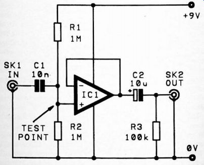
Fig.2.1 An example of a circuit which is very vulnerable to loading.
High sensitivity is not a factor that is always of great importance. When testing a high current circuit, such as the output of an audio power amplifier, the small amount of current tapped off by the meter should be totally insignificant. The same is not true of high impedance parts of a circuit. Consider the simple unity voltage gain buffer amplifier circuit of Figure 2.1. Resistors R1 and R2 bias the input of the amplifier to about half the supply voltage, or about 4.5 volts in this case. Measuring the output voltage of IC1 should give an accurate reflection of the voltage here, since even a low power operational amplifier can supply the milliamp or less required to drive an analog multimeter.
The situation is very different if the input voltage is measured. Connecting the negative test prod to the 0 volt supply rail in the usual way, and then connecting the positive test prod to the junction of R1, R2, etc., the resistance of the multimeter is effectively added in parallel with R2. Working out the resistance of R2. the test meter and then doing a little calculating will soon provide the effective resistance of R2.
We will not bother with any precise calculations here, but with using a 20k per volt multimeter on the 10 volt range to measure the voltage across R2, this gives 200k shunting Its effective resistance must therefore be something under 200k, and the measured voltage would be under one-sixth of the supply voltage (since the effective resistance of R2 would constitute less than one-sixth of the total resistance through R1 and R2). This would obviously result in a very low reading perhaps little more than 1 volt.
The reading is correct in that it is a true reflection of the voltage present at the test point, but it is erroneous in that it is only present while the multimeter is connected to the circuit. At other times the voltage will be completely different. Using a lower sensitivity multimeter such as a 1-k per volt type the situation would be even worse. There would probably be no significant deflection of the multi-meter's pointer at all! Again, the meter would be giving an accurate voltage reading, but one that was really totally misleading.
High-Resistance Voltmeter
Improved results can be obtained by using an amplifier ahead of the meter circuit so that the amount of current drawn from the circuit under test is reduced, and a robust meter of low sensitivity can then be used. This is basically all there is to a high resistance voltmeter. They do not usually work on the basis of using the amplifier to provide a sensitive current meter action, and then adding several switched series resistors to provide several ranges. The more normal method is to have a circuit which requires a negligible input current, and which has an input sensitivity of (say) 1 volt full scale. Other ranges are provided by adding a switched attenuator ahead of the basic 0 to 1 volt meter circuit. The sensitivity of the meter in ohms per volt terms is very much dependent on the resistance through the attenuator. Also, as the input resistance is fixed, the ohms per volt sensitivity varies from one range to the next.
High resistance voltmeters normally have an input resistance of about 10 or 11 megohms, and as a couple of examples, this would give at least 10M per volt sensitivity on the 1 volt range, and 1M per volt on the 10 volt range. This obviously compares very well with a conventional 20k per volt multimeter. On the higher voltage ranges the ohms per volt sensitivity of a high resistance voltmeter is less impressive. It would be 100k per volt on the 100 volt range for example, which is not vastly better than a standard 20k per volt multimeter, and no better than a few high sensitivity multimeters. However, sensitivity on high voltage ranges tends to be less important than it is on low voltage ranges. With modern low voltage circuits most users make little use of the higher d.c. voltage ranges anyway.
If we apply a high resistance voltmeter to our earlier example, by shunting 10 or 11 megohms across R2 in the test circuit we are only marginally reducing its effective value.
Readings will still be reduced by several percent, and loading is not a factor that can be totally ignored even when using a high resistance voltmeter, but there are few occasions when the degree of loading is large enough to give what could reasonably be considered misleading results.
High resistance analog multimeters used to be quite common, but are something of a rarity these days. One reason for this is the popularity of digital multimeters. These are really a form of high resistance voltmeter, and normally have an input resistance of 10 to 11 megohms. In use, they must therefore be regarded as high resistance voltmeters, and results should not be assessed on the basis of significant loading on the test point. Despite the popularity of digital multimeters, there are still plenty of users who find analog instruments quicker and easier to use. 1 must confess to preferring analog instruments in many respects, but the greater ruggedness of digital instruments is an asset that should not be overlooked. Analog instruments need to be treated with much greater respect if they are to provide long service.
The Circuit
This high resistance voltmeter is a simple three range analog type having full scale values of 0.5,5, and 50 volts. The input resistance is a little over 11 megohms. A definite advantage of digital multimeters over analog types is that the former will respond to voltages of either polarity, whereas the latter must be connected to the test points with the correct polarity.
This analog design borrows from digital multimeter design philosophy in this respect, and it will accept an input voltage of either polarity. This is especially helpful when making measurements on equipment which has dual balanced supply rails. With this type of equipment test points can be of either polarity with respect to the central 0 volt earth rail. Having a meter that will respond to inputs of either polarity could give rise to confusing results, but an optional input polarity indicator circuit enables the polarity of the input signal to be positively identified.
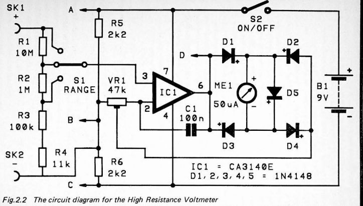
Figure 2.2
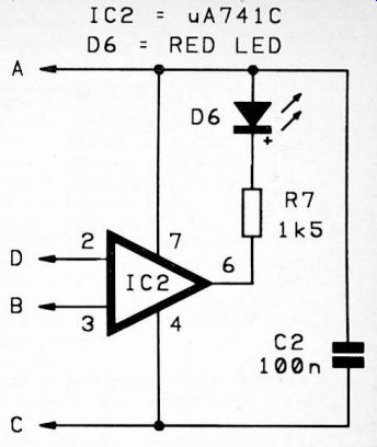
Figure 2.3
Figure 2.2 shows the full circuit diagram for the high resistance voltmeter. The optional input polarity indicator circuit is shown in Figure 2.3. The main circuit is a full wave active rectifier, and it uses the same basic configuration that was described in the previous Section. In this case the circuit does not need to provide high frequency operation, and there is no significant disadvantage in using silicon diodes in the bridge rectifier (D1 to D4). The advantages of silicon types is that they are cheaper and less easily damaged (particularly by heat when they are being soldered into circuit). D5 is a protection diode which ensures that the meter does not sustain any gross overloads. It might still be subjected to minor overloads, but any good quality meter should be able to take these without any risk of sustaining damage. VR1 is used to set the correct basic input sensitivity of 0.5 volts full scale.
The circuit is powered from a single 9 volt supply rather than the normal (for operational amplifier circuits) dual balanced supplies. R5 and R6 are used to effectively split the single 9 volt supply to provide dual 4.5 volt supplies. C1 provides negative feedback which severely limits the upper frequency response of the circuit. This helps to avoid problems with any electrical noise picked up in the test leads producing a strong deflection on ME1.
R1 to R4 plus S1 form a standard three step attenuator giving attenuation rates of 0dB, 20dB, and 40dB. This enables the basic 0.5 volt sensitivity of the circuit to be reduced by factors of ten and one hundred, so as to give the 5 and 50 volt ranges. IC1 is a MOS input operational amplifier that has an input resistance of over one million megohms. Thus, despite the high resistor values used in the attenuator, it does not significantly load the attenuator and reduce its accuracy.
The current consumption of the circuit is only a few milli-amps, and a PP3 size 9 volt battery is adequate as the power source. However, if the unit is likely to receive a great deal of use, it might be better to opt for a higher capacity battery, such as six HP7 size cells in a plastic holder or a PP9 size battery.
Although the polarity indicator circuit is not essential, 1 would certainly urge its inclusion in the unit. It will add little to the overall cost of the unit and will help to avoid possible confusion when using the unit. It is just an operational amplifier connected to operate as a straightforward voltage comparator. The two voltages it compares are the mid-supply bias level and the output voltage from IC1. If the output of IC1 goes positive, the inverting input of IC2 is taken higher in voltage than its non-inverting input. This sends the output of IC2 low and switches on LED indicator D6, If the output of IC1 goes negative, the comparative states of IC2's inputs are reversed, its output goes high, and D6 is switched off.
In other words, a positive input signal switches D6 on, and a negative input switches it off. The state of D6 under standby conditions is indeterminate, but due to noise on the output of IC1 it will probably switch on under standby conditions.
Note that if you would prefer D6 to have the opposite action (i.e. switch on when the input voltage is negative) simply reversing the connections to IC2's inputs will provide the desired action.
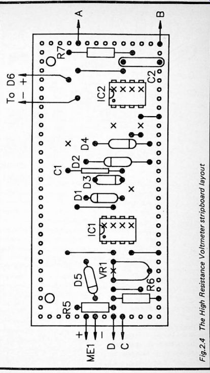
Fig. 2.4
Fig. 2.5
Construction
Details of the stripboard layout for the high resistance voltmeter project are provided in Figure 2.4, while the hard-wiring is shown in Figure 2.5. A stripboard having 31 holes by 14 copper strips is required. Construction of the board offers nothing out of the ordinary, but remember that IC1 is a MOS input device. Consequently, it must be Fitted in an 8 pin DIL holder and the other standard anti-static handling precautions should be observed. VR1 must be a miniature horizontal mounting preset if it is to fit into the board layout properly.
The attenuator resistors are mounted on S1 and not on the circuit board. Take care not to overheat these components and impair their accuracy when connecting them into circuit.
These resistors should have a tolerance of 2% or better. 1% resistors are probably worth the small extra cost. There should be little difficulty in fitting the unit into a plastic or metal box having dimensions of about 150 by 100 by 50 millimeters, but this obviously assumes that the meter used for ME1 is not a large type. A standard 60 millimeters by 40 millimeters (or similar) meter should be perfectly adequate, but the accuracy of the unit should be quite sufficient to justify a larger type if preferred.
The drive current for D6 is not very great, and I would recommend the use of a high brightness or ultra-bright LED for this component.
Components for Figures 2.2 and 2.3
Resistors (all 0.25 watt 5% unless noted)
10M 2% or better 1M 2% or better 100k 2% or better 11k 2%or better
R1 R2 R3 R4
2k2 R5 2k2 R6 1 k5 R7
Potentiometer
VR1 47k sub-miniature horizontal preset
Capacitors 100 nF polyester 100 nF ceramic C1 C2
Semiconductors IC1 CA3140E pA741C 1N4148 (5 off) 5mm panel LCD (high brightness type)
IC2 D1 to D5 D6
Miscellaneous
3 way 4 pole rotary (only 1 pole used)
SPST sub-miniature toggle 50pA moving coil panel meter 9 volt (e.g. PP3 size) S1 S2 ME1 B1
Case about 1 50 x 100 x 50mm
0.1 inch matrix stripboard 31 holes by 14 copper strips
Control knob
Battery connector
Wire, solder, printed circuit pins, etc.
Calibration
In order to calibrate the unit you need an accurately known voltage that is something approaching the full scale voltage of one of the unit's ranges. As an example, a 4.5 volt battery could be used to provide a calibration voltage for the 5 volt range of the unit. An ordinary multimeter would be used to measure the true voltage provided by the battery. The high resistance voltmeter would then be connected to the battery, after which VR1 would be adjusted to give the correct voltage reading on MEI. Start with the wiper of VR1 set well towards the end of its track which connects to IC1 pin 2 and C1. This avoids having an excessive deflection of the meter when the unit is connected to the calibration source.
Note that the circuit has protection for the meter, but there is no input overload protection. There is little risk of damaging the unit when testing low voltage circuits, or when it is switched to the 5 or 50 volt ranges. Be careful not to have the unit on the 0.5 volt range when measuring potentials of a around 10 volts or more.
Transistor Tester
Probably the biggest omission from the repertoire of most multimeters is any means of testing components other than resistors and diodes. A few instruments have some form of built-in transistor tester, and a very few have capacitance measuring ranges, but most have no provision for testing either type of component. A transistor tester is one of the most useful pieces of test gear for the electronics enthusiast, and is something that can be built at quite low cost. Only a handful of components are required for a basic transistor tester, and the cost of the unit is largely dependent on the quality of the meter movement used. As high accuracy is not usually considered to be of prime importance for a transistor tester, a low cost type should be perfectly suitable.
Fig. 2.6 N. P. N. and P. N. P. transistor test circuits
Gain and Leakage
The basic setup for testing the d.c. current gain ("HFE" in transistor specifications) of a transistor is shown in Figure 2.6.
Note that NPN and PNP transistors require different test circuits, and that these two configurations are shown in Figure 2.6(a) and Figure 2.6(b) respectively.
If we take the NPN test circuit first, the supply is applied to the collector and emitter terminals of the test transistor with the appropriate polarity, and a meter (ME1) is used to monitor the current flow. A base current is supplied to the device via base resistor R1, with this component limiting the current to a suitable level. This level would normally be quite low -- say about 1 to 100 microamps. The base current causes a much larger collector current to flow, and the current gain of a transistor is equal to its collector current divided by its base current. Thus, the higher the gain of the test transistor, the higher the reading on ME1. In fact ME1 can be calibrated directly in terms of current gain, and as a linear scale is obtained. no difficult recalibration of the meter is needed. Of course, this assumes that a suitable base current is chosen so that the current reading on ME1 is easily converted into the corresponding value for current gain.
It is not too difficult to arrange things in this way. For example, if a base current of 1 micro-amp is used, and ME1 has a full scale value of 1 milliamp (1000 microamps), the tester will have a full scale value of 1000. In other words, if the current reading in milliamps is translated into microamps, this gives the gain of the test device (which is equal to the collector current in microamps). Converting a reading of (say) 0.45 milliamps to a gain reading of 450 times is not a particularly complex process.
By having more than one base current available it is possible to give the unit several measuring ranges. If we extend our earlier example, using a base current of 10 micro- amps instead of 1 microamp would reduce the full scale value by a factor of ten. This must be so, as with ten times the base current only one-tenth of the current gain is then needed in order to produce full scale deflection of the meter. Switching to a base current of 10 microamps would therefore give a full scale (current gain) value of 100 times. This would provide much better accuracy on low gain devices which would produce little deflection of the meter with a lull scale value of 1000 times.
The PNP test circuit is essentially the same as the NPN type. As before, an input current is supplied to the base terminal of the test transistor via a current limiting resistor, and a meter monitors the flow of current in the collector circuit. The only difference is that the supply polarity must be reversed. Also, as a result of tins, the polarity of the meter must be reversed so that it is fed with a signal that provides forwards deflection of its pointer.
A crucial factor that has been overlooked solar is that of leakage through the test component. Obviously the collector to emitter resistance of the test transistor will not be infinite, and some current will flow between these two terminals even with no base current applied. For silicon transistors this leakage current will normally be too small to be of significance. A typical maximum leakage current for a silicon transistor would be 1 microamp, and a typical small signal silicon transistor might have a leakage level of perhaps 50 nanoamps (0.05 microamps). Germanium transistors tend to have relatively high leakage currents, with levels as high as one or two milliamps being acceptable in many cases. Some germanium power devices have quoted maximum acceptable leakage levels of around 100 milliamps! Leakage currents are important for two reasons. Firstly, their effect on current gain readings must be taken into account. A transistor might be found to give quite a high current gain reading, but this would be deceptive if the leakage current was almost sufficient to give this gain reading. In order to obtain a realistic current gain figure the collector current must be reduced by an amount equal to the leakage current. In other words, the gain of a transistor is not really equal to the collector current divided by the base current. It is equal to the increase in collector current when a base current is applied, divided by that base current. Fortunately, in virtually all cases the leakage current is so low as to be of no consequence, and it can be ignored The second reason for the leakage level being important is that it is often a strong pointer to whether or not a transistor is serviceable. This is especially the case with silicon transistors. where the leakage level is normally very low. If a silicon transistor is found to have a significant leakage level it almost certainly means that the device is unusable. Even if the gain of the device should be found to be quite acceptable, it is probably not worth using the component. It is quite likely to have other problems such as a high noise level, and reliability is unlikely to be very good. The data sheets for silicon transistors almost invariably quote very low maximum leakage levels, and any device which exceeds its leakage quota should be regarded with considerable suspicion.
Measuring the leakage current of a transistor is very easy, and simply requires a slight modification to the gain measuring setup. Either a switch should be included in the base circuit so that the base current can be switched off, or the base leadout wire can simply be left unconnected.
The Circuit
The full circuit diagram for the transistor tester appears in Figure 2.7. It follows the basic configuration of Figure 2.6 quite closely, but obviously NPN/PNP switching has had to be incorporated. In fact any switching of this type for the meter has been avoided by incorporating a bridge rectifier here (D1 to D4). Whatever the polarity of the supply, two of the four diodes will always channel the current through the meter with the correct polarity. R4 is a current limiting resistor, and it ensures that the current through the meter is limited to a safe level (just under 2 milliamps) in the event of the test device being closed circuit. This permits a maximum overload on the meter of something approaching 100%, but this should not be sufficient to damage any moving coil meter, even if sustained for a long period of time.
S1 is the npn/pnp switch. Its three poles are used to provide supply polarity switching for the base, emitter, and collector terminals of the test device. There are three switched base resistors (R1 to R3) which provide base currents of approximately npn/pnp, and 10uA. With ME1 having a full scale value of 1mA, this gives full scale (current gain) readings of 1000, 250, and 100. S3 is the range switch. S2 can be used to cut off the base current so that a leakage current check can be made.
S4 is the on/off switch, and it is not strictly necessary.
Under standby conditions the current consumption of the unit is zero anyway! However, it is good practice to include an on/off switch on any piece of equipment. This ensures that the battery is not run down unnecessarily if (say) a couple of the test prods should become short circuited while the unit is not in use. I have prematurely exhausted several sets of multimeter batteries in this way by leaving the instrument set to a resistance range. When in use the current consumption, except under meter overload conditions, never exceeds 1 milliamp. A small 9 volt battery such as a PP3 type is perfectly adequate as the power source.
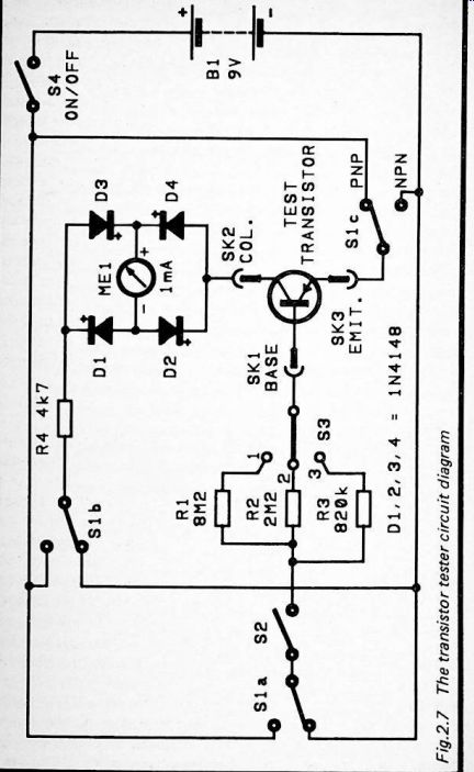
Fig. 2.7
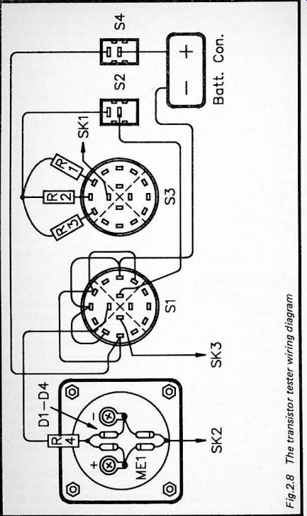
Fig. 2.8
Construction
With so few components, and such a large proportion of those components being panel mounted types such as switches and sockets, the use of a circuit board is not really justified. The unit can be hard-wired without too much difficulty. Figure 2.8 shows the wiring diagram for the transistor tester.
The best size of case for the unit is largely dependent on the size of the meter used. Assuming that a small type of about 60 by 40 millimeters is utilized, it should be possible to fit the unit into a plastic box having dimensions of about 150 by 100 by 50 millimeters. It is not essential to lay-out the front panel in the arrangement shown in Figure 2.8, but try to have things arranged sensibly so that a minimal number of long trailing wires are required.
There are a number of options available for SK1 to SK3.
One of these is to mount a transistor socket on the front panel. This is convenient in that it should be possible to fit virtually any transistor into it without too much difficulty, but is awkward in that these sockets are not intended for panel mounting, and would probably be difficult to fix to the panel securely. A good alternative is a three way DIN socket. Most transistors can be plugged into one of these, and it is easy to make up a set of test leads to accommodate those that will not. The test leads merely consist of three short pieces of multi-strand (PVC insulated) connecting wire fitted with a 3 way DIN plug at one end and three crocodile clips at the other. Use leads and (or) crocodile clips of different colors so that you can easily identify which is which. Another alternative is to fix three 1 millimeter sockets on the front panel in a triangular pattern. These can be used in much the same way as a 3 way DIN socket, but have the advantage that the test transistor should connect to them somewhat more easily and reliably. A final alternative is to simply drill a hole in the front panel for three short crocodile clip leads which are then hard-wired to the main unit. Once again, the leads and (or) the clips should be of different colors to permit easy identification.
Wiring up the unit is only likely to be a bit difficult because few constructors are familiar with this method of construction these days. Before fitting any of the components or adding in any of the wiring I would strongly recommend that all the tags should be tinned with solder. At least, those tags that are actually used should be tinned with solder. Only one pole of S3 is used, which leaves some twelve tags unused. Three poles of S1 are used, but it must be a type having an adjustable end-stop, which in this case is set for two way operation. This leaves seven tags of S1 unused. Note that S1 must be a "break before make" type, not a "make before break" switch. The latter would cause a momentary short circuit on the supply lines each time the switch was operated. This would almost certainly result in a very short contact life.
Construction is almost certainly easiest if all the components are fitted prior to adding any of the wiring. Add the two pairs of diodes on to ME1 (making sure their polarity is correct) and then add the two connections to complete the ring. Then add R4 and fit R1 to R3 onto S3. This should all be quite easy provided the ends of the component leads are tinned with solder before connecting them. Next add the links that join certain pins of S1, and then add the point-to- point wiring plus the battery clip. This wiring must all be insulated in order to avoid any accidental short circuits. In fact I used non-insulated single strand wires for the links on S1, and this is an easy way of completing this wiring. However, if you do things this way you must be careful to route the links where they are well separated from one another, or PVC sleeving must be fitted over them.
Components for Figure 2.7
Resistors (all 0.25W 5%) 8M2 R1 R2 2M2 R3 820k 4k7 R4
Semiconductors
D1 1N4148
1N4148
1N4148
1N4148
D2 D3 D4
Miscellaneous:
ME1 1mA moving coil panel meter 3 way 4 pole rotary with adjustable end- stop (set for 2 way operation, only 3 poles used)
SPST sub-miniature toggle 3 way 4 pole rotary (only one pole used)
SPST sub-miniature toggle 9 volt (PP3 size)
3 way DIN socket (see text)
S1 S2 S3 S4 B1 SK1,2,3
Case about 150 x 100 x 50mm
Two control knobs
Battery connector
Wire, solder, etc.
In Use
Using the unit is basically quite simple, and it is just a matter of switching on, setting S1 for NPN or PNP operation (as appropriate), connecting the test device correctly, checking the leakage current (S2 set open), and then measuring the gain of the device by setting S2 to the closed position. It is best to start with S3 at position 1 (the 0 to 1000 range), and to switch to one of the other ranges if a very low reading is obtained. It is unlikely that the test transistor will be damaged if S1 is set to the wrong mode, but due care should be exercised when testing germanium transistors. These are generally much less hardy than the more common silicon types. Of course, if the wrong mode is used it is quite likely that a "dud" will be indicated even if the test component is fully operational. When a "dud" device is indicated, always double check the control settings and connections to the device before discarding it.
Although using the unit is very straightforward, interpreting results is not necessarily as easy. In most cases it is, but some transistors are difficult to test. The high leakage levels of some germanium transistors and the difficulties they present were discussed earlier. Just what readings indicate a "dud" and what represents satisfactory test results are to some extent a matter of subjective judgment. It is possible for the leakage test to give an off-scale reading, but for the test device to be perfectly satisfactory. This is most likely to occur with power devices, and the leakage levels of small signal germanium transistors tend to be significant but still quite modest.
Fortunately, germanium transistors are now largely obsolete, and you may never need to test one with the unit.
When testing any transistors using the unit you must bear in mind that current gains in data sheets are normally specified at certain collector voltages and currents. This tester does not provide checks at specific collector currents and voltages.
Both depend on the meter indication obtained. The collector current is simply the one indicated on the meter. For instance, with the unit set to the 0 to 1000 range, and a reading of 0.45 milliamps being displayed, this represents a gain of 450 at a collector current of 0.45 milliamps (450 microamps). The collector voltage varies from about 8 volts at low readings to about 3 volts or so at high readings.
This is not all of academic importance. The gain of a transistor varies with changes in both collector current and voltage. Variations caused by changes in collector voltage tend to be relatively small, but changes in gain due to alterations in the collector current can be (and often are) quite substantial.
In general, the gain of a transistor increases as its collector current is raised. This property is easily demonstrated by measuring the gain of a low gain transistor on the lowest and the highest ranges of the unit. The gain value indicated when using the 0 to 1000 range will almost certainly be much lower, due to the very much lower collector current that flows.
What this means in practice is that readings may well be slightly lower than the data sheets would suggest, simply because the transistors are being tested at lower collector currents. A marginally low gain reading could be indicative of a faulty component, but would be more likely to indicate that the device is at the low end of its gain range but acceptable in this respect. Power transistors are the ones where problems are most likely to be experienced. These generally have their current gains specified at quite high currents, and are only designed to work efficiently at these high currents.
Quite low gain readings do not necessarily indicate a faulty device when checking power devices, but a gain reading that is only a small fraction of the minimum requirement probably does. If you are likely to test a lot of power devices it would be beneficial to have higher test currents. This is easily achieved by using a 10 milliamp meter for ME1, and reducing all four resistor values by a factor of ten. The only problem with doing this is that few component suppliers seem to stock a large range of panel meters these days, and a 10 milliamp type could be difficult to track down.
When using the unit you must bear in mind that it only provides approximate gain readings. This is all that is required in most cases as faulty transistors arc not usually a little low in gain. Most faults produce a very low gain level. In fact in many cases faulty transistors are open or closed circuit, with the base terminal exercising no control on the collector current whatever.
Capacitance Meter
As pointed out in the previous section of this Section dealing with the transistor tester, a serious omission from the repertoire of most multimeters is some means of measuring capacitance.
It is possible to make a few basic tests on capacitors using the resistance range of a multimeter, but this really boils down to little more than checking that the test component has not developed a fault in its dielectric which has caused it to go closed circuit. With high value components it takes some time for the multimeter to charge the capacitor, and for the reading to go to a very high level With a little experience the time taken for the reading to go off-scale can give a good idea of the test component's value. However, this simple test procedure only works reasonably well with high value capacitors, and does not normally work at all with capacitors of less than a few tens of nanofarads in value.
With so many capacitors used in electronic circuits, a capacitance meter is a decided asset for the electronics hobbyists' workshop. Units that provide a high degree of accuracy over a very wide capacitance range tend to be quite complex and expensive to build. For most purposes though, a unit that does not cover the highest and lowest value capacitors will suffice, and can be built at quite a modest cost. This unit has five capacitance ranges with full scale values of 1-n, 10n, 100 nF, 1uF, and 10uF. Accuracy is very good except on the lowest range, where stray capacitance compromises results at the low value end of the range. The unit can still be used to test capacitors having values from a few tens of picofarads up to 10 microfarads. As explained previously, most multimeters can be used to check high value capacitors. This only leaves very low value capacitors un-catered for, and these are not used to any great extent in most types of modern electronic circuit. This unit plus a multimeter should therefore be capable of checking the vast majority of capacitors that you use.
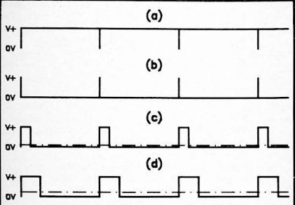
Fig.2.9 Capacitance meter example waveforms.
Pulse Duration
Capacitance meters can operate on a variety of principles, but most simple units arc based on a monostable multivibrator.
The duration of the output pulse from the monostable is dependent on the values of the timing capacitor and the timing resistor. The pulse length is proportional to the values of both components. In this application the timing capacitance is the component under test, and the timing resistance is a reference component. This gives an output pulse duration that is proportional to the value of the test component, but some means of converting pulse length into a proportional meter reading is required.
This is actually quite easy, and can be achieved by using an oscillator to trigger the monostable at a fixed frequency.
The waveforms of Figure 2.9 help to explain the manner in which this gives the desired action. An important point to keep in mind here is that a moving coil panel meter fed with a pulse signal will not be able to follow the changes in input voltage unless they are at a very low frequency. With an input frequency of more than about 10Hz to 20Hz the meter registers the average input voltage.
In this example the waveform of (a) represents the very brief trigger pulses from the clock oscillator. The waveform of (b) is the output signal from the monostable with no test capacitor connected. Stray capacitance prevents a pulse width of zero from being obtained, but the pulses are so short as to give a negligible average output voltage. In (c) a test capacitor is connected, and it gives a mark space ration of 1 to 7. This in turn gives an average output voltage equal to one-eighth of the supply voltage (as indicated by the dot-dash line), since the output is low for 87.5% of the time and high for the other 12.5%. In (d) a test capacitor of double the previous value has been connected to the unit, and the longer pulse duration has resulted in a mark-space ratio of 1 to 3.
The average output voltage is now 25% of the supply voltage, as the output of the monostable is high for 25% of the time.
In other words, a doubling of the test capacitance has doubled the average output voltage.
Provided the pulse duration does not become excessively long, this gives the required pulse duration to voltage conversion. If the pulse duration should become excessive, the result is a sort of frequency divider action, with the mono-stable only triggering on (say) every second clock pulse. The average output voltage drops back to a relatively low level if this should happen. However, provided the output pulse duration never exceeds the period of one clock cycle, the desired action with good linearity is obtained.
The Circuit
Figure 2.10 shows the full circuit diagram for the capacitance meter, which is based on a couple of the ever popular 555 timer integrated circuits (IC1 and IC2). In fact these are an "improved" version of the standard 555, the TLC555P. This is a low power version of the 555, but in this case it is the higher speed and lower self-capacitance that are of prime importance. These help to improve performance on the lowest range. The self-capacitance of a standard 555 seems to be around 50p, whereas the TLC555P would seem to have a self-capacitance that is usually well under 20p. This ensures that any deflection of the meter under standby conditions on range 1 is too low to greatly detract from the accuracy of the unit.
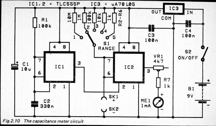
Figure 2.10
IC1 is the clock oscillator, and accordingly it is operated in the astable mode. It is not quite the standard astable configuration in that there would normally be a resistor between pins 6 and 7 of the device. This sets the discharge rate of the timing capacitor (C2), or the low period for each output cycle in other words. In this application the output signal must be a series of negative pulses that are as narrow as possible. The salient point here is that the 555 when operated in the monostable mode is a re-triggerable type. This means that the output pulse cannot be shorter than the input trigger pulse. Consequently, it is essential to have the trigger pulse very short in order to obtain good accuracy at low readings.
IC2 is the monostable, and five switched reference resistors (R2 to R6) provide the unit with its five measuring ranges. ME1 is the panel meter which is driven from the output of IC2, and VR1 enables the sensitivity of the meter to be adjusted for calibration purposes. It is crucial that the unit is powered from a very well stabilized supply. Any variations in the supply voltage will be reflected in corresponding changes in readings. The unit is powered from a 9 volt battery, but monolithic voltage regulator IC3 stabilizes this to produce a well regulated 5 volt output for the main circuit. The current consumption is only a few milliamps, and a small (PP3 size) 9 volt battery is perfectly adequate as the power source.
Construction
Details of the stripboard component panel are provided in Figure 2.11. A board having 32 holes by 15 copper strips is required. Construction of the board offers little that is out of the ordinary. Although IC1 and IC2 are CMOS components, they have built-in anti-static protection circuits that render any special handling precautions unnecessary. I would still recommend the use of 8 pin DIL holders for these components though. Note that they are mounted "upside-down" (i.e. pm 1 and the notch of each device are at the bottom not the top). A dozen link wires are required - be careful not to overlook any of them. Printed circuit pins are fitted to the board at the points where connections to off-board components will eventually be made.
As with the other projects that use a meter, the best size for the case depends to a large extent on the size of the meter used. For a unit that incorporates a standard 60 x 40 millimeter panel meter, or one of about this size, a plastic box having dimensions of about 150 by 100 by 50 millimeters should suffice. The exact layout used is far from critical, but try to arrange things so that the leads from the board to SK1 and SK2 are no longer than is really necessary.
The off-board components include R2 to R6 which are mounted on S1. The point-to-point style wiring is shown in Figure 2.12. Fit the resistors onto S1 first and then add in the other wiring. Try not to let the resistors get any hotter than is really necessary, as heat could impair their accuracy. In order to ensure good accuracy on all ranges it is important to use resistors having a tolerance of no more than 2%, and 1% components are preferable.
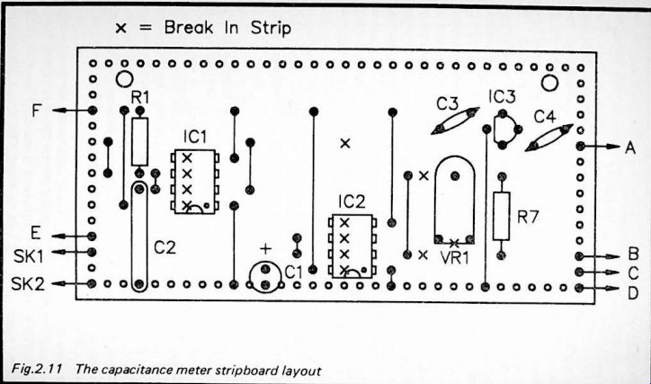
Figure 2.11
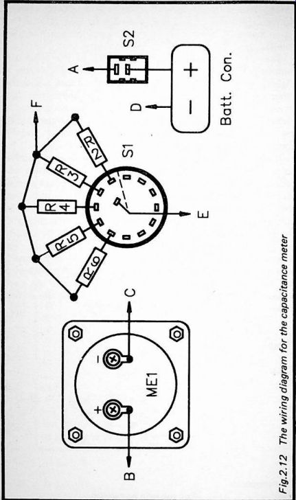
Figure 2.12
If SK1 and SK2 are a couple of 1 millimeter sockets mounted close together on the front panel, many capacitors will connect to them directly. For those that will not, a pair of short crocodile clip leads must be made up. It is important that these leads are quite short (preferably no more than 50 millimeters long), as long leads could reduce the accuracy of the unit with low value capacitors. The unit can be used to test polarised (electrolytic and tantalum capacitors), but these components must be connected the right way round if reliable results arc to be obtained. The positive leadout is the one that connects to SK1. It is a good idea to use a red socket for SK1 and a black one for SK2, so that the correct polarity is clearly indicated.
Components for Figure 2.10
Resistors (all 0.25W 5% unless noted)
100k 10M 1 or 2% 1M 1 or 2% 100k 1 or 2% 10k 1 or 2% 1-k 1 or 2%
R1 R2 R3 R4 R5 R6 R7
1-k Potentiometer VR1 4k7 sub-min hor preset
Capacitors
10u 25V radial elect
330n polyester
100 nF ceramic
100 nF ceramic
C1 C2 C3 C4
Semiconductors
IC1 TLC555P
TLC 555P
uA78L05 (5V 100mA positive regulator)
IC2
IC3
Miscellaneous
ME1 1 mA moving coil panel meter
9 volt (PP3 size)
1 pole 12 way with adjustable end-stop (set for 5 way operation)
SPST sub-min toggle
1 mm socket (red)
1 mm socket (black)
Case about 150 x 100 x 50 millimeters
Stripboard having 32 holes by 15 copper strips
Battery connector
Control knob
Two 8 pin DIL IC holders
Wire, solder, etc.
B1 S1 S2 SK1 SK2
Calibration
The first point that must be made is that the unit should never be used to test a capacitor that is charged up. This is especially important when testing high value or high voltage components. This is not just a failing of this capacitance meter - virtually all instruments of this type are vulnerable to damage from charged-up test components. The simplest solution to the problem is to short circuit the leads of each test component together prior to connecting them to the capacitance meter. A metal plate fixed to the top panel of the unit can be used for components that have short lead-outs which can not be connected together.
A better solution is to have an extra pair of sockets and test leads, with a 33 ohm current limiting resistor wired between the two sockets. This will provide a more gradual (but still quite rapid) discharge that will avoid the sparking that occurs with a simple short circuit of the capacitor. Of course, it is only when testing a capacitor that has just been removed from a piece of equipment that has recently been powered-up that there is any great danger of the test capacitor holding a significant charge. On the other hand, it does no harm to always play safe and ensure that test components are fully discharged. Bear in mind that high voltage capacitors are extremely dangerous when charged up, and that they may retain their charge for some considerable period of time after the equipment in which they are installed has been switched off. Only those with suitable experience should attempt to remove and test a component of this type.
In order to calibrate the unit you require a close tolerance (1 or 2%) capacitor having a value equal to the full scale value of one range of the capacitance meter. It is not a good idea to calibrate the unit on range 1 as the accuracy on this range is not quite as good as that obtained on the other ranges. Calibration on ranges 4 and 5 cannot be recommended either. Close tolerance capacitors having a value of or 10uF could be difficult to obtain, and extremely expensive indeed if you could find sources of supply. Calibration on range 2 using a 10n capacitor or range 3 using a 100n component are more practical propositions.
The calibration process merely involves switching on the unit and setting it to the appropriate range, connecting the calibration capacitor to SK1 and SK2. and then adjusting VR1 for precisely full scale deflection of the meter.
When testing capacitors using any capacitance meter, bear in mind that the tolerances of many capacitors are quite high.
In particular, ceramic and electrolytic types can have tolerances as large as plus 100% and minus 50%. Relatively few types seem to offer tolerances of less than 20%. With some capacitors a substantial error in value is therefore quite acceptable.
AF Frequency Meter
The ideal piece of test gear for frequency measurement is a digital instrument having a wide range of gate times, and with the capability of operating at frequencies of up to at least a few hundred megahertz. Unfortunately, despite general reductions in the prices of electronic equipment, high quality digital frequency meters (d.f.m.s) remain quite expensive. In fact the lowest cost d.f.m.s are still far from cheap.
For audio frequency measurement an analog frequency meter, based on an ordinary moving coil panel meter, is often capable of giving sufficiently accurate results. Apart from use as a test instrument for frequency measuring applications, a unit of this type can be very useful as a frequency readout for an audio frequency signal generator. It is particularly useful for operation in conjunction with a home constructed audio signal generator where providing an accurately calibrated frequency scale can be difficult and very time consuming.
This audio frequency meter covers frequencies up to 100kHz. It has four ranges with full scale values of 100Hz, 1 kHz, 10kHz, and 100kHz. It is quite sensitive, and requires a minimum input level of under 10 millivolts peak-to-peak in order to function properly. A trigger circuit ensures that the unit cuts out if the input level is inadequate, rather than giving a low and erroneous reading. The input impedance is quite high at about 500 kilohms (it is inevitably somewhat lower at high frequencies due to the shunting effect of the input capacitance).
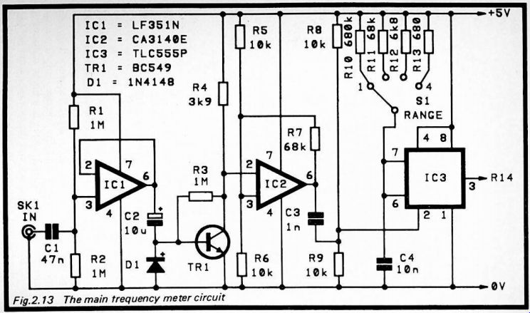
Figure 2.13
Basic Operation
The basic way in which the unit functions is very similar to the system used in the capacitance meter project described previously. The output from a mono-stable is fed to a volt-meter circuit that registers the average output voltage. The difference is that in this case the pulse duration of the monostable is fixed, and it is the trigger frequency that alters.
The trigger frequency is, of course, equal to the frequency of the input signal. With a low input frequency there is a large gap from one pulse to the next, and the average output voltage is low. With a much higher input frequency the pulses become bunched together and the average output voltage becomes much higher. In fact there is a linear relationship between the input frequency and the average output voltage, giving the required frequency to voltage conversion. Although this is a very simple method of voltage to frequency conversion, at the low frequencies involved in audio applications it gives very good linearity, and is not easily bettered.
The Circuit
Figure 2.13 shows the main circuit diagram for the analog frequency meter. The meter and regulator circuits are shown separately in Figure 2.14.
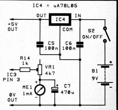
Fig.2.14
The regulator and meter sections of the frequency meter IC1 acts as the basis of the input stage which is a simple operational amplifier voltage follower circuit. This provides no voltage gain, but provides the unit with a high input impedance. TR1 operates in the common emitter mode, and this provides most of the circuit's voltage gain (over 40dB of voltage gain in fact). IC2 is a Schmitt trigger circuit with hysteresis provided by R7. This stage ensures that the monostable is not triggered at all if the input signal is marginally too low, so that low and misleading readings arc avoided. It also helps to avoid multiple triggering if an unusual or badly noise infested waveform is applied to the input. Bear in mind though, that the hysteresis has only a limited effect. A lot of noise on the input signal could result in misleading results. A really unusual input waveform might also defeat the hysteresis, but it is debatable whether waveforms with double peaks etc. can really be said to have a single frequency. With most waveforms the unit will give perfectly accurate results.
IC3 is the monostable, and this uses the standard 555 configuration. C4 is the timing capacitor, while R10 to R13 are four switched timing resistors that provide the unit with its four measuring ranges. The meter circuit includes preset resistor VR1 which enables the unit to be calibrated against a known input frequency. At low input frequencies many moving coil meters get a severe case of the "pointer jitters". This can be a very severe problem indeed if the input frequency happens to hit one at which the meter movement exhibits a mechanical resonance. It is a problem that is much more noticeable with some meters than with others. C7 smooths out the pulses to give a reasonably ripple-free signal across the meter so that any "jitter" problems are avoided.
Like the capacitance meter project, this one must be fed from a well stabilized supply if good accuracy is to be maintained. The circuit is therefore fed from the 9 volt battery supply by way of a 5 volt regulator circuit based on IC4. The current consumption of the unit is just a few milliamps, and a small (PP3 size) 9 volt battery is quite adequate as the power source.
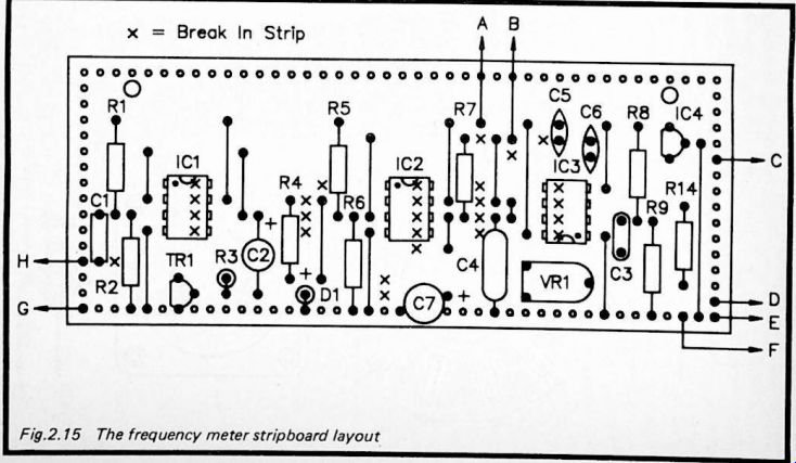
Fig. 2.15
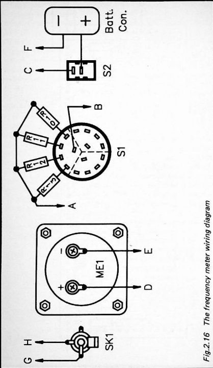
Fig. 2.16
Construction
Details of the stripboard layout for the analog frequency meter are provided in Figure 2.15. This requires a board having 41 holes by 16 copper strips. The wiring diagram is shown in Figure 2.16. Construction is much along the lines of the other projects in this Section, and there is little that merits any special mention. Note though that IC3 has the opposite orientation to the other two 8 pin DIL integrated circuits.
Be careful to fit it the right way round. IC2 is a MOS input device that consequently requires the standard anti-static handling precautions to be observed. In Figure 2.16 it is assumed that SK1 is a standard 3.5 millimeter jack socket, but any other type of audio/test equipment connector could be used here if preferred. S1 is one pole of a standard 4 way 3 pole rotary switch. Construction is easier if C1 has 7.5 millimeter lead spacing and C3 has 5 millimeter lead spacing.
Otherwise it could be difficult to fit these components into the layout. Ideally C4 should be a type which has fairly long leadouts, but if necessary extension leads can be soldered to it.
Components for Figures 2.13 and 2.14
Resistors (all 0.25W 5% unless noted)
R1 1M R2 1M R3 1M R4 3k9 10k R5 10k R6 68k R7 10kR8 10k R9 680k 1 or 2% 68k 1 or 2% 6k8 1 or 2% 680 1 or 2% R10 R11 R12 R13 1-k R14
Potentiometer
VR1 4k7 sub-min hor preset
Capacitors
47n polyester (7.5 mm lead spacing)
10u 25V radial elect In mylar (5mm lead spacing)
10n polyester (C280) C1 C2 C3 C4
C5 100n ceramic
100n ceramic 470m 10V radial elect
C6 C7
Semiconductors
IC1 LF351N CA3140E TLC555P MA78L05 (5V 100mA reg) BC549 1N4148 IC2 IC3 IC4 TR1 D1 Miscellaneous
4 way 3 pole rotary (only one pole used)
SPST sub-min toggle 9 volt (PP3 size) 1mA moving coil panel meter 3.5mm jack socket S1 S2 B1 ME1 SK1
Case about 150 x 100 x 50mm
Stripboard having 41 holes by 16 copper strips
Control knob Battery connector Three 8 pin DIL integrated circuit holders
Wire, solder, etc.
Calibration
In order to calibrate the unit you must have access to a signal at a known frequency that will give 50 to 100% deflection of the meter on any range of the unit. Ideally a calibration oscillator or an accurately calibrated audio signal generator would be used to provide the calibration signal. In the absence of suitable test equipment an electronic musical instrument should suffice. For example, the A above middle A is at a frequency of 880Hz. This could be used to calibrate the unit on range 2. Simply couple the input of the instrument to SK1, then get a helper to play the A above middle A on the instrument while you adjust VR1 for a reading of 880Hz.
When using the unit keep in mind that inputs of more than a few volts peak-to-peak could cause overloading, which could possibly lead to inaccurate results. In an extreme case the input circuit of the unit could be overloaded to the point where it sustains damage. The unit can only be used to test high signal levels if it is used in conjunction with a probe having a built-in attenuator. Oscilloscope probes having an integral 20dB switchable attenuator are ideal, but far from cheap. A test probe having a series resistor of about 33k should be adequate to ensure correct operation and prevent damage on any high level input signals that are likely to be encountered.