AMAZON multi-meters discounts AMAZON oscilloscope discounts
The electronics that go along with the physical sensor element are often very important to the overall device. The sensor electronics can limit the performance, cost, and range of applicability. If carried out properly, the design of the sensor electronics can allow the optimal extraction of information from a noisy signal.
Most sensors do not directly produce voltages but rather act like passive devices, such as resistors, whose values change in response to external stimuli. In order to produce voltages suitable for input to microprocessors and their analog-to-digital converters, the resistor must be "biased" and the output signal needs to be "amplified."
Types of Sensors
Resistive sensor circuits
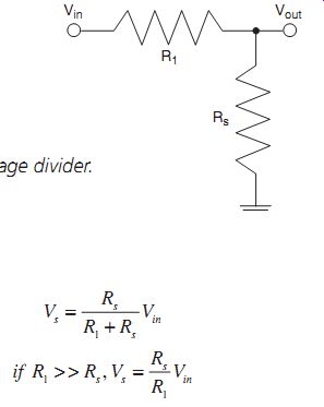
FIG. 1.1: Voltage divider.
Resistive devices obey Ohm's law, which states that the voltage across a resistor is equal to the product of the current flowing through it and the resistance value of the resistor. It is also required that all of the current entering a node in the circuit leave that same node. Taken together, these two rules are called Kirchhoff's Rules for Circuit Analysis, and these may be used to determine the currents and voltages throughout a circuit.
For the example shown in FIG. 1.1, this analysis is straightforward. First, we recognize that the voltage across the sense resistor is equal to the resistance value times the current. Second, we note that the voltage drop across both resistors (Vin-0) is equal to the sum of the resistances times the current. Taken together, we can solve these two equations for the voltage at the output. This general procedure applies to simple and complicated circuits; for each such circuit, there is an equation for the voltage between each pair of nodes, and another equation that sets the current into a node equal to the current leaving the node. Taken all together, it is always possibly to solve this set of linear equations for all the voltages and currents. So, one way to measure resistance is to force a current to flow and measure the voltage drop. Current sources can be built in number of ways. One of the easiest current sources to build consists of a voltage source and a stable resistor whose resistance is much larger than the one to be measured. The reference resistor is called a load resistor. Analyzing the connected load and sense resistors as shown in FIG. 1.1, we can see that the cur rent flowing through the circuit is nearly constant, since most of the resistance in the circuit is constant. Therefore, the voltage across the sense resistor is nearly proportional to the resistance of the sense resistor.
As stated, the load resistor must be much larger than the sense resistor for this circuit to offer good linearity. As a result, the output voltage will be much smaller than the input voltage. Therefore, some amplification will be needed.
A Wheatstone bridge circuit is a very common improvement on the simple voltage divider. It consists simply of the same voltage divider in FIG. 1.1, combined with a second divider composed of fixed resistors only. The point of this additional divider is to make a reference voltage that is the same as the output of the sense voltage divider at some nominal value of the sense resistance. There are many complicated additional features that can be added to bridge circuits to more accurately compensate for particular effects, but for this discussion, we'll concentrate on the simplest designs- the ones with a single sense resistor, and three other bridge resistors that have resistance values that match the sense resistor at some nominal operating point.
The output of the sense divider and the reference divider are the same when the sense resistance is at its starting value, and changes in the sense resistance lead to small differences between these two volt ages. A differential amplifier (such as an instrumentation amplifier) is used to produce the difference between these two voltages and amplify the result. The primary ad vantages are that there is very little offset voltage at the output of this differential amplifier, and that temperature or other effects that are common to all the resistors are automatically compensated out of the resulting signal. Eliminating the offset means that the small differential signal at the output can be amplified without also amplifying an offset voltage, which makes the design of the rest of the circuit easier.
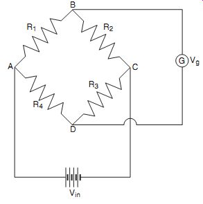
FIG. 1.2: Wheatstone bridge circuit.
Capacitance measuring circuits
Many sensors respond to physical signals by producing a change in capacitance. How is capacitance measured? Essentially, all capacitors have an impedance given by impedance
…where f is the oscillation frequency in Hz, w is in rad/sec, and C is the capacitance in farads. The i in this equation is the square root of -1, and signifies the phase shift between the current through a capacitor and the voltage across the capacitor.
Now, ideal capacitors cannot pass current at DC, since there is a physical separation between the conductive elements. However, oscillating voltages induce charge oscillations on the plates of the capacitor, which act as if there is physical charge flowing through the circuit. Since the oscillation reverses direction before substantial charges accumulate, there are no problems. The effective resistance of the capacitor is a meaningful characteristic, as long as we are talking about oscillating voltages.
With this in mind, the capacitor looks very much like a resistor. Therefore, we may measure capacitance by building voltage divider circuits as in FIG. 1.1, and we may use either a resistor or a capacitor as the load resistance. It is generally easiest to use a resistor, since inexpensive resistors are available which have much smaller temperature coefficients than any reference capacitor. Following this analogy, we may build capacitance bridges as well. The only substantial difference is that these circuits must be biased with oscillating voltages. Since the "resistance" of the capacitor depends on the frequency of the AC bias, it is important to select this frequency carefully. By doing so, all of the advantages of bridges for resistance measurement are also available for capacitance measurement.
However, providing an AC bias can be problematic. Moreover, converting the AC signal to a DC signal for a microprocessor interface can be a substantial issue. On the other hand, the availability of a modulated signal creates an opportunity for use of some advanced sampling and processing techniques. Generally speaking, voltage oscillations must be used to bias the sensor. They can also be used to trigger voltage sampling circuits in a way that automatically subtracts the voltages from opposite clock phases. Such a technique is very valuable, because signals that oscillate at the correct frequency are added up, while any noise signals at all other frequencies are subtracted away. One reason these circuits have become popular in recent years is that they can be easily designed and fabricated using ordinary digital VLSI fabrication tools. Clocks and switches are easily made from transistors in CMOS circuits. There fore, such designs can be included at very small additional cost-remember that the oscillator circuit has to be there to bias the sensor anyway.
Capacitance measuring circuits are increasingly implemented as integrated clock/ sample circuits of various kinds. Such circuits are capable of good capacitance measurement, but not of very high performance measurement, since the clocked switches inject noise charges into the circuit. These injected charges result in voltage offsets and errors that are very difficult to eliminate entirely. Therefore, very accurate capacitance measurement still requires expensive precision circuitry.
Since most sensor capacitances are relatively small (100 pF is typical), and the measurement frequencies are in the 1-100 kHz range, these capacitors have impedances that are large (> 1 megohm is common). With these high impedances, it is easy for parasitic signals to enter the circuit before the amplifiers and create problems for extracting the measured signal. For capacitive measuring circuits, it is therefore important to minimize the physical separation between the capacitor and the first amplifier. For microsensors made from silicon, this problem can be solved by integrating the measuring circuit and the capacitance element on the same chip, as is done for the ADXL311 mentioned above.
Inductance measurement circuits
Inductances are also essentially resistive elements. The "resistance" of an inductor is given by XL = 2pfL, and this resistance may be compared with the resistance of any other passive element in a divider circuit or in a bridge circuit as shown in FIG. 1.1. Inductive sensors generally require expensive techniques for the fabrication of the sensor mechanical structure, so inexpensive circuits are not generally of much use. In large part, this is because inductors are generally three-dimensional devices, consisting of a wire coiled around a form. As a result, inductive measuring circuits are most often of the traditional variety, relying on resistance divider approaches.
Sensor Limitations
Limitations in resistance measurement
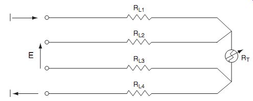
FIG. 1.3: Lead compensation.
¦ Lead resistance - The wires leading from the resistive sensor element have a resistance of their own. These resistances may be large enough to add errors to the measurement, and they may have temperature dependencies that are large enough to matter. One useful solution to the problem is the use of the so-called 4-wire resistance approach (FIG. 1.3). In this case, current (from a current source as in FIG. 1.1) is passed through the leads and through the sensor element. A second pair of wires is independently attached to the sensor leads, and a voltage reading is made across these two wires alone.
It is assumed that the voltage-measuring instrument does not draw significant current (see next point), so it simply measures the voltage drop across the sensor element alone. Such a 4-wire configuration is especially important when the sensor resistance is small, and the lead resistance is most likely to be a significant problem.
¦ Output impedance - The measuring network has a characteristic resistance which, simply put, places a lower limit on the value of a resistance which may be connected across the output terminals without changing the output volt age. For example, if the thermistor resistance is 10 k-ohm and the load resistor resistance is 1 M-ohm, the output impedance of this circuit is approximately 10 k-ohm If a 1 k-ohm resistor is connected across the output leads, the output voltage would be reduced by about 90%. This is because the load applied to the circuit (1 k-ohm) is much smaller than the output impedance of the circuit (10 k-ohm), and the output is "loaded down." So, we must be concerned with the effective resistance of any measuring instrument that we might attach to the output of such a circuit. This is a well-known problem, so measuring instruments are often designed to offer maximum input impedance, so as to minimize loading effects. In our discussions we must be careful to arrange for instrument input impedance to be much greater than sensor output impedance.
Limitations to measurement of capacitance
¦ Stray capacitance - Any wire in a real-world environment has a finite capacitance with respect to ground. If we have a sensor with an output that looks like a capacitor, we must be careful with the wires that run from the sensor to the rest of the circuit. These stray capacitances appear as additional capacitances in the measuring circuit, and can cause errors. One source of error is the changes in capacitance that result from these wires moving about with respect to ground, causing capacitance fluctuations which might be confused with the signal. Since these effects can be due to acoustic pressure-induced vibrations in the positions of objects, they are often referred to as microphonics. An important way to minimize stray capacitances is to minimize the separation between the sensor element and the rest of the circuit. Another way to minimize the effects of stray capacitances is mentioned later-the virtual ground amplifier.
Filters
Electronic filters are important for separating signals from noise in a measurement.
The following sections contain descriptions of several simple filters used in sensor based systems.
¦ Low pass - A low-pass filter (FIG. 1.4) uses a resistor and a capacitor in a voltage divider configuration. In this case, the "resistance" of the capacitor decreases at high frequency, so the output voltage decreases as the input frequency increases. So, this circuit effectively filters out the high frequencies and "passes" the low frequencies.
The mathematical analysis is as follows:
Using the complex notation for the impedance, let
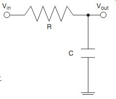
FIG. 1.4: Low-pass filter.
Using the voltage divider equation in FIG. 1.1
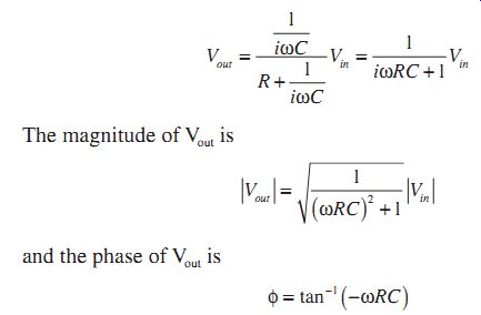
¦ High-pass - The high-pass filter is exactly analogous to the low-pass filter, except that the roles of the resistor and capacitor are reversed. The analysis of a high-pass filter is as follows:
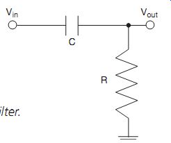
FIG. 1.5: High-pass filter.
Similar to a low-pass filter,
The magnitude is
…and the phase is ...
¦ Bandpass - By combining low-pass and high-pass filters together, we can create a bandpass filter that allows signals between two preset oscillation frequencies. Its diagram and the derivations are as follows:
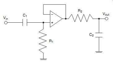
FIG. 1.6: Band-pass filter.
Let the high-pass filter have the oscillation frequency ?1 and the low-pass filter have the frequency ohm such that
Then the relation between V and V is ….
The operational amplifier in the middle of the circuit was added in this circuit to isolate the high-pass from the low-pass filter so that they do not effectively load each other. The op-amp simply works as a buffer in this case. In the following section, the role of the op-amps will be discussed more in detail.
Operational amplifiers
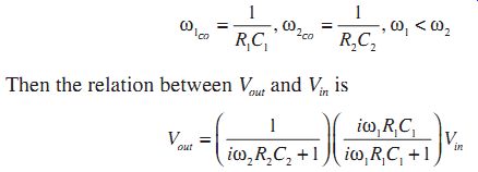
Operational amplifiers (op-amps) are electronic devices that are of enormous generic use for signal processing. The use of op-amps can be complicated, but there are a few simple rules and a few simple circuit building blocks which designers need to be familiar with to understand many common sensors and the circuits used with them.
An op-amp is essentially a simple 2-input, 1-output device. The output voltage is equal to the difference between the non-inverting input and the inverting input multiplied by some extremely large value (10^5 ). Use of op-amps as simple amplifiers is uncommon.
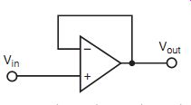
FIG. 1.7: Non-inverting unity gain amplifier.
Feedback is a particularly valuable concept in op-amp applications. For instance, consider the circuit shown in FIG. 1.6, called the follower configuration. Notice that the inverting input is tied directly to the output. In this case, if the output is less than the input, the difference between the inputs is a positive quantity, and the output voltage will be increased. This adjustment process continues, until the output is at the same voltage as the non-inverting input. Then, everything stays fixed, and the output will follow the voltage of the non-inverting input. This circuit appears to be useless until you consider that the input impedance of the op-amp can be as high as 10^9 ohms, while the output can be many orders of magnitude smaller. Therefore, this follower circuit is a good way to isolate circuit stages with high output impedance from stages with low input impedance.
This op-amp circuit can be analyzed very easily, using the op-amp golden rules:
1. No current flows into the inputs of the op-amp.
2. When configured for negative feedback, the output will be at whatever value makes the input voltages equal.
Even though these golden rules only apply to ideal operational amplifiers, op-amps can in most cases be treated as ideal. Let's use these rules to analyze more circuits:
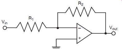
FIG. 1.8: Inverting amplifier.
FIG. 1.8 shows an example of an inverting amplifier. We can derive the equation by taking the following steps.
1. Point B is ground. Therefore, point A is also ground. (Rule 2)
2. Since the current flowing from Vin to Vout is constant (Rule 1), Vout/R2 = -Vin/R1
3. Therefore, voltage gain = Vout/Vin = -R2/R1
FIG. 1.9: Non-inverting amplifier.
FIG. 1.9 illustrates another useful configuration of an op-amp. This is a non-inverting amplifier, which is a slightly different expression than the inverting amplifier.
Taking it step-by-step,
1. Va = Vin (Rule 2)
2. Since Va comes from a voltage divider, Va = (R1/(R1 + R2)) Vout
3. Therefore, Vin = (R1/(R1 + R2)) Vout
4. Vout/Vin = (R1 + R2)/R1 = 1 + R2/R1
The following section provides more details on sensor systems and signal conditioning.
1.2 Sensor Systems
This section deals with sensors and associated signal conditioning circuits. The topic is broad, but the focus here is to concentrate on the sensors with just enough coverage of signal conditioning to introduce it and to at least imply its importance in the overall system.
Strictly speaking, a sensor is a device that receives a signal or stimulus and responds with an electrical signal, while a transducer is a converter of one type of energy into another. In practice, however, the terms are often used interchangeably.
Sensors and their associated circuits are used to measure various physical proper ties such as temperature, force, pressure, flow, position, light intensity, etc. These properties act as the stimulus to the sensor, and the sensor output is conditioned and processed to provide the corresponding measurement of the physical property. We will not cover all possible types of sensors here, only the most popular ones, and specifically, those that lend themselves to process control and data acquisition systems.
Sensors do not operate by themselves. They are generally part of a larger system consisting of signal conditioners and various analog or digital signal processing circuits. The system could be a measurement system, data acquisition system, or process control system, for example.
Sensors may be classified in a number of ways. From a signal conditioning viewpoint it is useful to classify sensors as either active or passive. An active sensor requires an external source of excitation. Resistor-based sensors such as thermistors, RTDs (Resistance Temperature Detectors), and strain gages are examples of active sensors, because a current must be passed through them and the corresponding voltage measured in order to determine the resistance value. An alternative would be to place the devices in a bridge circuit; however, in either case, an external current or voltage is required.
On the other hand, passive (or self-generating) sensors generate their own electrical output signal without requiring external voltages or currents. Examples of passive sensors are thermocouples and photodiodes which generate thermoelectric voltages and photocurrents, respectively, which are independent of external circuits. It should be noted that these definitions (active vs. passive) refer to the need (or lack thereof) of external active circuitry to produce the electrical output signal from the sensor. It would seem equally logical to consider a thermocouple to be active in the sense that it produces an output voltage with no external circuitry. However, the convention in the industry is to classify the sensor with respect to the external circuit requirement as defined above.
SENSORS:
Convert a Signal or Stimulus (Representing a Physical Property) into an Electrical Output
TRANSDUCERS:
Convert One Type of Energy into Another
The Terms are often Interchanged Active Sensors Require an External Source of Excitation: RTDs, Strain-Gages Passive (Self-Generating) Sensors do not: Thermocouples, Photodiodes, Piezoelectrics
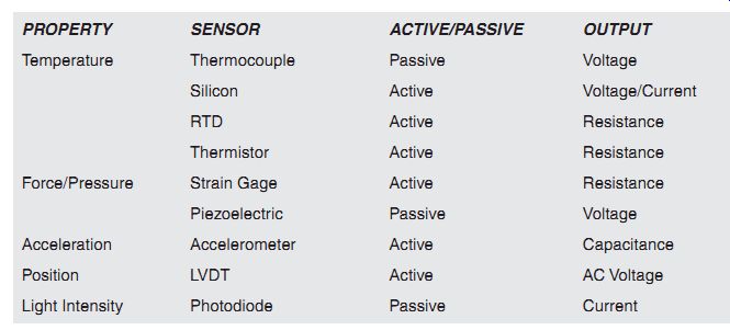
FIG. 2.1: Sensor overview. FIG. 2.2: Typical sensors and their outputs
A logical way to classify sensors-and the method used throughout the remainder of this book-is with respect to the physical property the sensor is designed to measure.
Thus, we have temperature sensors, force sensors, pressure sensors, motion sensors, etc. However, sensors which measure different properties may have the same type of electrical output. For instance, a resistance temperature detector (RTD) is a variable resistance, as is a resistive strain gage. Both RTDs and strain gages are often placed in bridge circuits, and the conditioning circuits are therefore quite similar. In fact, bridges and their conditioning circuits deserve a detailed discussion.
The full-scale outputs of most sensors (passive or active) are relatively small voltages, currents, or resistance changes, and therefore their outputs must be properly conditioned before further analog or digital processing can occur. Because of this, an entire class of circuits have evolved, generally referred to as signal conditioning circuits.
Amplification, level translation, galvanic isolation, impedance transformation, linearization, and filtering are fundamental signal conditioning functions that may be required.
Whatever form the conditioning takes, however, the circuitry and performance will be governed by the electrical character of the sensor and its output. Accurate characterization of the sensor in terms of parameters appropriate to the application, e.g., sensitivity, voltage and current levels, linearity, impedances, gain, offset, drift, time constants, maximum electrical ratings, and stray impedances and other important considerations can spell the difference between substandard and successful application of the device, especially in cases where high resolution and precision, or low-level measurements are involved.
Higher levels of integration now allow ICs to play a significant role in both analog and digital signal conditioning. ADCs (analog-to-digital converters) specifically designed for measurement applications often contain on-chip programmable-gain amplifiers (PGAs) and other useful circuits, such as current sources for driving RTDs, thereby minimizing the external conditioning circuit requirements.
Most sensor outputs are nonlinear with respect to the stimulus, and their outputs must be linearized in order to yield correct measurements. Analog techniques may be used to perform this function. However, the recent introduction of high performance ADCs now allows linearization to be done much more efficiently and accurately in software and eliminates the need for tedious manual calibration using multiple and sometimes interactive trimpots.
The application of sensors in a typical process control system is shown in FIG. 2.3. Assume the physical property to be controlled is the temperature. The output of the temperature sensor is conditioned and then digitized by an ADC. The microcontroller or host computer determines if the temperature is above or below the desired value, and outputs a digital word to the digital-to-analog converter (DAC). The DAC output is conditioned and drives the actuator, in this case a heater. Notice that the interface between the control center and the remote process is via the industry-standard 4-20mA loop.
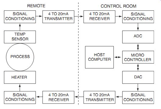
FIG. 2.3: Typical industrial process control loop.
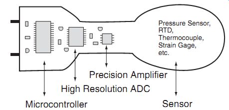
FIG. 2.5: Basic elements in a smart sensor.
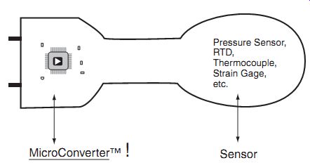
FIG. 2.6: The even smarter sensor.
NEXT: Application Considerations
PREV: