AMAZON multi-meters discounts AMAZON oscilloscope discounts
4. Signal Conditioning High Impedance Sensors
Many popular sensors have output impedances greater than several M-ohm, and the associated signal conditioning circuitry must be carefully designed to meet the challenges of low bias current, low noise, and high gain. A large portion of this section is devoted to the analysis of a photodiode preamplifier.
This application points out many of the problems associated with high impedance sensor signal conditioning circuits and offers practical solutions which can be applied to practically all such sensors. Other examples of high impedance sensors discussed are piezoelectric sensors, charge output sensors, and charge coupled devices (CCDs).
Photodiode Preamplifier Design
Photodiodes generate a small current which is proportional to the level of illumination.
They have many applications ranging from precision light meters to high-speed fiber optic receivers.
The equivalent circuit for a photodiode is shown in FIG. 4.3.
One of the standard methods for specifying the sensitivity of a photodiode is to state its short circuit photocurrent (Isc) at a given light level from a well defined light source. The most commonly used source is an incandescent tungsten lamp running at a color temperature of 2850K. At 100 fc (foot candles) illumination (approximately the light level on an overcast day), the short circuit current is usually in the picoamps to hundreds of microamps range for small area (less than 1mm^2 ) diodes.

FIG. 4.1: High impedance sensors.

FIG. 4.2: Photodiode applications.
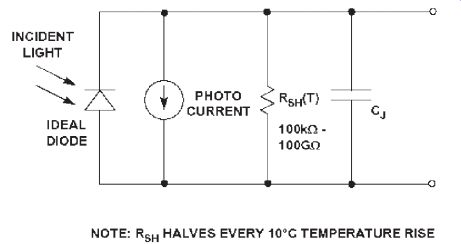
FIG. 4.3: Photodiode equivalent circuit.
[...]
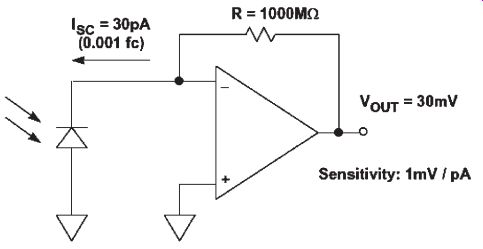
FIG. 4.7: Current-to-voltage converter (simplified).
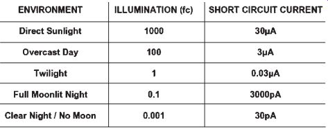
FIG. 4.6: Short circuit current versus light intensity for photodiode
(photovoltaic mode).
A convenient way to convert the photodiode current into a usable voltage is to use an op amp as a current-to-voltage converter as shown in FIG. 4.7. The diode bias is maintained at zero volts by the virtual ground of the op amp, and the short circuit current is converted into a voltage. At maximum sensitivity, the amplifier must be able to detect a diode current of 30 pA. This implies that the feedback resistor must be very large, and the amplifier bias current very small. For example, 1000 M-ohm will yield a corresponding voltage of 30 mV for this amount of current. Larger resistor values are impractical, so we will use 1000 M-ohm for the most sensitive range. This will give an output voltage range of 10 mV for 10pA of diode current and 10 V for 10 nA of diode current. This yields a range of 60 dB. For higher values of light intensity, the gain of the circuit must be reduced by using a smaller feedback resistor. For this range of maximum sensitivity, we should be able to easily distinguish between the light intensity on a clear moonless night (0.001fc) and that of a full moon (0.1fc)! Notice that we have chosen to get as much gain as possible from one stage, rather than cascading two stages. This is in order to maximize the signal-to-noise ratio (SNR). If we halve the feedback resistor value, the signal level decreases by a factor of 2, while the noise due to the feedback resistor (4 kTR. Bandwidth) decreases by only 2. This reduces the SNR by 3 dB, assuming the closed loop bandwidth remains constant. Later in the analysis, we will see that the resistors are one of the largest contributors to the overall output noise.
To accurately measure photodiode currents in the tens of picoamps range, the bias current of the op amp should be no more than a few picoamps. This narrows the choice considerably. The industry-standard OP07 is an ultra-low offset voltage (10 µV) bipolar op amp, but its bias current is 4 nA (4000 pA!). Even super-beta bipolar op amps with bias current compensation (such as the OP97) have bias currents on the order of 100 pA at room temperature, but may be suitable for very high temperature applications, as these currents do not double every 10ºC rise like FETs. A FET-input electrometer-grade op amp is chosen for our photodiode preamp, since it must operate only over a limited temperature range. FIG. 4.8 summarizes the performance of several popular "electrometer grade" FET input op amps. These devices are fabricated on a BiFET process and use P-Channel JFETs as the input stage (see FIG. 4.9). The rest of the op amp circuit is designed using bipolar devices.
The BiFET op amps are laser trimmed at the wafer level to minimize offset voltage and offset voltage drift. The offset voltage drift is minimized by first trimming the input stage for equal currents in the two JFETs which comprise the differential pair. A second trim of the JFET source resistors minimizes the input offset voltage. The AD795 was selected for the photodiode preamplifier, and its key specifications are summarized in FIG. 4.10.
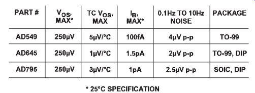
FIG. 4.8: Low bias current precision BiFET op amps (electrometer grade).
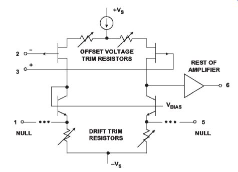
FIG. 4.9: BiFET op amp input stage.

FIG. 4.10: AD795 BiFET op amp key specifications.
Since the diode current is measured in terms of picoamperes, extreme attention must be given to potential leakage paths in the actual circuit. Two parallel conductor stripes on a high-quality well-cleaned epoxy-glass PC board 0.05 inches apart running parallel for 1 inch have a leakage resistance of approximately 1011 ohms at +125°C. If there is 15 volts between these runs, there will be a current flow of 150 pA.
The critical leakage paths for the photodiode circuit are enclosed by the dotted lines in FIG. 4.11. The feedback resistor should be thin film on ceramic or glass with glass insulation. The compensation capacitor across the feedback resistor should have a polypropylene or polystyrene dielectric.
All connections to the summing junction should be kept short. If a cable is used to connect the photodiode to the preamp, it should be kept as short as possible and have Teflon insulation.
Guarding techniques can be used to reduce parasitic leakage currents by isolating the amplifier's input from large voltage gradients across the PC board. Physically, a guard is a low impedance conductor that surrounds an input line and is raised to the line's voltage. It serves to buffer leakage by diverting it away from the sensitive nodes.
The technique for guarding depends on the mode of operation, i.e., inverting or non-inverting. FIG. 4.12 shows a PC board layout for guarding the inputs of the AD795 op amp in the DIP ("N") package. Note that the pin spacing allows a trace to pass between the pins of this package. In the inverting mode, the guard traces surround the inverting input (pin 2) and run parallel to the input trace. In the follower mode, the guard voltage is the feedback voltage to pin 2, the inverting input. In both modes, the guard traces should be located on both sides of the PC board if at all possible and connected together.
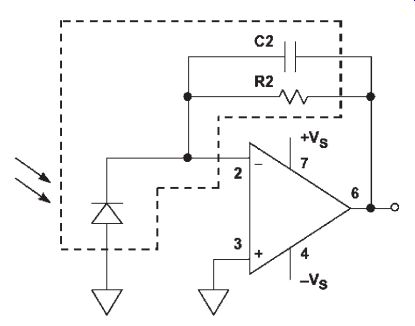
FIG. 4.11: Leakage current paths.
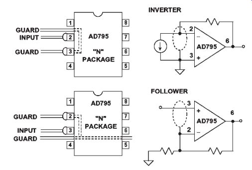
FIG. 4.12: PCB layout for guarding DIP package.
Things are slightly more complicated when using guarding techniques with the SOIC surface mount ("R") package because the pin spacing does not allow for PC board traces between the pins. FIG. 4.13 shows the preferred method. In the SOIC "R" package, pins 1, 5, and 8 are "no connect" pins and can be used to route signal traces as shown. In the case of the follower, the guard trace must be routed around the -VS pin.
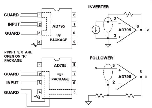
FIG. 4.13: PCB layout for guarding SOIC package.
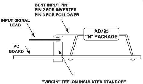
FIG. 4.14: Input pin connected to "virgin" Teflon insulated
standoff.
For extremely low bias current applications (such as using the AD549 with an input bias current of 100 fA), all connections to the input of the op amp should be made to a virgin Teflon standoff insulator ("Virgin" Teflon is a solid piece of new Teflon material which has been machined to shape and has not been welded together from powder or grains). If mechanical and manufacturing considerations allow, the invert ing input pin of the op amp should be soldered directly to the Teflon standoff (see FIG. 4.14) rather than going through a hole in the PC board. The PC board itself must be cleaned carefully and then sealed against humidity and dirt using a high quality conformal coating material.
In addition to minimizing leakage currents, the entire circuit should be well shielded with a grounded metal shield to prevent stray signal pickup.
Preamplifier Offset Voltage and Drift Analysis
An offset voltage and bias current model for the photodiode preamp is shown in FIG. 4.15. There are two important considerations in this circuit. First, the diode shunt resistance (R1) is a function of temperature-it halves every time the temperature increases by 10ºC. At room temperature (+25ºC) , R1 = 1000 M-ohm, but at +70ºC it decreases to 43 M-ohm. This has a drastic impact on the circuit DC noise gain and hence the output offset voltage. In the example, at +25ºC the DC noise gain is 2, but at +70ºC it increases to 24.
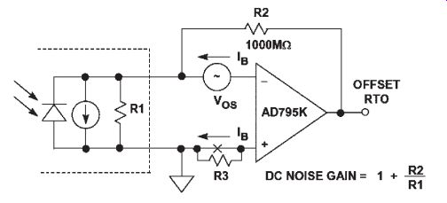
FIG. 4.15: AD795 preamplifier DC offset errors.
The second difficulty with the circuit is that the input bias current doubles every 10ºC rise in temperature. The bias current produces an output offset error equal to IBR2.
At +70ºC the bias current increases to 24 pA compared to its room temperature value of 1 pA. Normally, the addition of a resistor (R3) between the non-inverting input of the op amp and ground having a value of R1||R2 would yield a first-order cancellation of this effect. However, because R1 changes with temperature, this method is not effective. In addition, the bias current develops a voltage across the R3 cancellation resistor, which in turn is applied to the photodiode, thereby causing the diode response to become nonlinear.
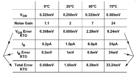
FIG. 4.16: AD795K preamplifier total output offset error.
The total referred to output (RTO) offset voltage errors are summarized in FIG. 4.16. Notice that at +70ºC the total error is 33.24 mV. This error is acceptable for the design under consideration. The primary contributor to the error at high temperature is of course the bias current. Operating the amplifier at reduced supply voltages, minimizing output drive requirements, and heat sinking are some ways to reduce this error source. The addition of an external offset nulling circuit would minimize the error due to the initial input offset voltage.
Thermoelectric Voltages as Sources of Input Offset Voltage
Thermoelectric potentials are generated by electrical connections which are made between different metals at different temperatures. For example, the copper PC board electrical contacts to the kovar input pins of a TO-99 IC package can create an off set voltage of 40 µV/ºC when the two metals are at different temperatures. Common lead-tin solder, when used with copper, creates a thermoelectric voltage of 1 to 3 µV/ºC. Special cadmium-tin solders are available that reduce this to 0.3 µV/ºC.
The solution to this problem is to ensure that the connections to the inverting and non-inverting input pins of the IC are made with the same material and that the PC board thermal layout is such that these two pins remain at the same temperature. In the case where a Teflon standoff is used as an insulated connection point for the inverting input (as in the case of the photodiode preamp), prudence dictates that connections to the non-inverting inputs be made in a similar manner to minimize possible thermoelectric effects.
Preamplifier AC Design, Bandwidth, and Stability
The key to the preamplifier AC design is an understanding of the circuit noise gain as a function of frequency. Plotting gain versus frequency on a log-log scale makes the analysis relatively simple (see FIG. 4.17). This type of plot is also referred to as a Bode plot. The noise gain is the gain seen by a small voltage source in series with the op amp input terminals. It is also the same as the non-inverting signal gain (the gain from "A" to the output). In the photodiode preamplifier, the signal current from the photodiode passes through the C2/R2 network. It is important to distinguish between the signal gain and the noise gain, because it is the noise gain characteristic which determines stability regardless of where the actual signal is applied.
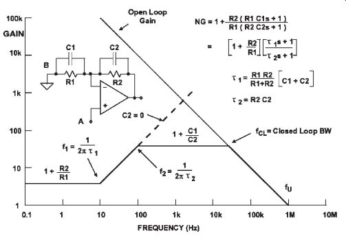
FIG. 4.17: Generalized noise gain (NG) Bode plot.
Stability of the system is determined by the net slope of the noise gain and the open loop gain where they intersect. For unconditional stability, the noise gain curve must intersect the open loop response with a net slope of less than 12 dB/octave (20 dB per decade). The dotted line shows a noise gain which intersects the open loop gain at a net slope of 12dB/octave, indicating an unstable condition. This is what would occur in our photodiode circuit if there were no feedback capacitor (i.e., C2 = 0).
The general equations for determining the break points and gain values in the Bode plot are also given in FIG. 4.17. A zero in the noise gain transfer function occurs at a frequency of 1/2pt1, where t1 = R1||R2(C1 + C2). The pole of the transfer function occurs at a corner frequency of 1/2pt2, where t2 = R2C2 which is also equal to the signal bandwidth if the signal is applied at point "B". At low frequencies, the noise gain is 1 + R2/R1. At high frequencies, it is 1 + C1/C2. Plotting the curve on the log- log graph is a simple matter of connecting the breakpoints with a line having a slope of 45º. The point at which the noise gain intersects the op amp open loop gain is called the closed loop bandwidth. Notice that the signal bandwidth for a signal applied at point "B" is much less, and is 1/2pR2C2.
FIG. 4.18 shows the noise gain plot for the photodiode preamplifier using the actual circuit values. The choice of C2 determines the actual signal bandwidth and also the phase margin. In the example, a signal bandwidth of 16 Hz was chosen.
Notice that a smaller value of C2 would result in a higher signal bandwidth and a corresponding reduction in phase margin. It is also interesting to note that although the signal bandwidth is only 16 Hz, the closed loop bandwidth is 167 kHz. This will have important implications with respect to the output noise voltage analysis to follow.
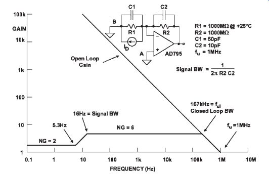
FIG. 4.18: Noise gain of AD795 preamplifier at 25°C.
It is important to note that temperature changes do not significantly affect the stability of the circuit. Changes in R1 (the photodiode shunt resistance) only affect the low frequency noise gain and the frequency at which the zero in the noise gain response occurs. The high frequency noise gain is determined by the C1/C2 ratio.
Photodiode Preamplifier Noise Analysis
To begin the analysis, we consider the AD795 input voltage and current noise spectral densities shown in FIG. 4.19. The AD795 performance is truly impressive for a JFET input op amp: 2.5 µV p-p 0.1 Hz to 10 Hz noise, and a 1/f corner frequency of 12 Hz, comparing favor ably with all but the best bipolar op amps. As shown in the figure, the current noise is much lower than bipolar op amps, making it an ideal choice for high impedance applications.
The complete noise model for an op amp is shown in FIG. 4.20. This model includes the reactive elements C1 and C2. Each individual output noise contributor is calculated by integrating the square of its spectral density over the appropriate frequency bandwidth and then taking the square root:
RMS Output Noise Due to V V f df 1 1 2
= ( ) ohm Eq. 4.1
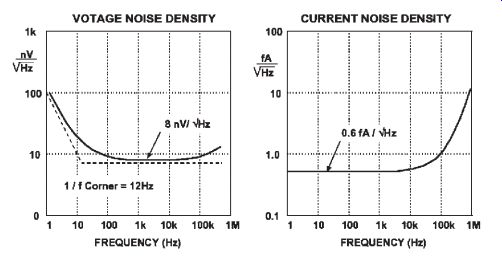
FIG. 4.19: Voltage and current noise of AD795.
In most cases, this integration can be done by inspection of the graph of the individual spectral densities superimposed on a graph of the noise gain. The total output noise is then obtained by combining the individual components in a root sum-squares manner. The table below the diagram in FIG. 4.20 shows how each individual source is reflected to the output and the corresponding bandwidth for integration. The factor of 1.57 (p/2) is required to convert the single pole bandwidth into its equivalent noise bandwidth. The resistor Johnson noise spectral density is given by:
V kTR R = 4
Eq. 4.2
...where k is Boltzmann's constant (1.38 × 10^-23 J/K) and T is the absolute temperature in K. A simple way to compute this is to remember that the noise spectral density of a 1 k-ohm resistor is 4 nV_/Hz at +25ºC. The Johnson noise of another resistor value can be found by multiplying by the square root of the ratio of the resistor value to 1000 ohm. Johnson noise is broadband, and its spectral density is constant with frequency.
Input Voltage Noise In order to obtain the output voltage noise spectral density plot due to the input volt age noise, the input voltage noise spectral density plot is multiplied by the noise gain plot. This is easily accomplished using the Bode plot on a log-log scale. The total RMS output voltage noise due to the input voltage noise is then obtained by integrating the square of the output voltage noise spectral density plot and then taking the square root. In most cases, this integration may be approximated. A lower frequency limit of 0.01 Hz in the 1/f region is normally used. If the bandwidth of integration for the input voltage noise is greater than a few hundred Hz, the input voltage noise spectral density may be assumed to be constant. Usually, the value of the input volt age noise spectral density at 1 kHz will provide sufficient accuracy.
It is important to note that the input voltage noise contribution must be integrated over the entire closed loop bandwidth of the circuit (the closed loop bandwidth, fcl , is the frequency at which the noise gain intersects the op amp open loop response). This is also true of the other noise contributors which are reflected to the output by the noise gain (namely, the non-inverting input current noise and the non-inverting input resistor noise).
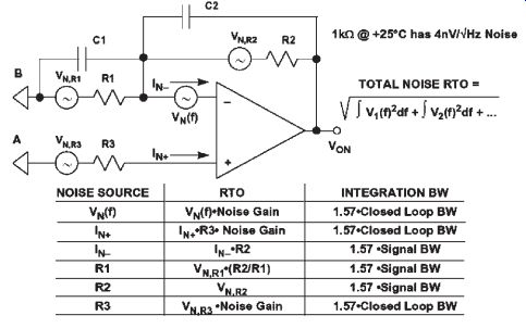
FIG. 4.20: Amplifier noise model.
The inverting input noise current flows through the feedback network to produce a noise voltage contribution at the output The input noise current is approximately constant with frequency, therefore, the integration is accomplished by multiplying the noise current spectral density (measured at 1 kHz) by the noise bandwidth which is 1.57 times the signal bandwidth (1/2pR2C2). The factor of 1.57 (p/2) arises when single-pole 3 dB bandwidth is converted to equivalent noise bandwidth.
High Impedance Sensors
Johnson Noise Due to Feedforward Resistor R1
The noise current produced by the feedforward resistor R1 also flows through the feedback network to produce a contribution at the output. The noise bandwidth for integration is also 1.57 times the signal bandwidth.
Non-Inverting Input Current Noise
The non-inverting input current noise, IN+, develops a voltage noise across R3 which is reflected to the output by the noise gain of the circuit. The bandwidth for integration is therefore the closed loop bandwidth of the circuit. However, there is no contribution at the output if R3 = 0 or if R3 is bypassed with a large capacitor which is usually desirable when operating the op amp in the inverting mode.
Johnson Noise Due to Resistor in Non-Inverting Input
The Johnson voltage noise due to R3 is also reflected to the output by the noise gain of the circuit. If R3 is bypassed sufficiently, it makes no significant contribution to the output noise.
Summary of Photodiode Circuit Noise Performance
FIG. 4.21 shows the output noise spectral densities for each of the contributors at +25ºC. Note that there is no contribution due to IN+ or R3 since the non inverting input of the op amp is grounded.
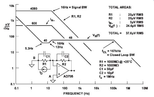
FIG. 4.21: Ouput voltage noise components spectral densities (nV_/Hz)
at +25°C.
Noise Reduction Using Output Filtering
From the above analysis, the largest contributor to the output noise voltage at +25ºC is the input voltage noise of the op amp reflected to the output by the noise gain. This contributor is large primarily because the noise gain over which the integration is per formed extends to a bandwidth of 167 kHz (the intersection of the noise gain curve with the open-loop response of the op amp). If the op amp output is filtered by a single pole filter (as shown in FIG. 4.22) with a 20 Hz cutoff frequency (R = 80 M-ohm, C = 0.1 µF), this contribution is reduced to less than 1 µV rms. Notice that the same results would not be achieved simply by increasing the feedback capacitor, C2. Increasing C2 lowers the high frequency noise gain, but the integration bandwidth becomes proportionally higher. Larger values of C2 may also decrease the signal bandwidth to unacceptable levels. The addition of the simple filter reduces the output noise to 28.5 µV rms; approximately 75% of its former value. After inserting the filter, the resistor noise and current noise are now the largest contributors to the output noise.
Summary of Circuit Performance
The diagram for the final optimized design of the photodiode circuit is shown in FIG. 4.22. Performance characteristics are summarized in FIG. 4.23. The total output voltage drift over 0 to +70ºC is 33 mV. This corresponds to 33 pA of diode current, or approximately 0.001 foot-candles. (The level of illumination on a clear moonless night). The offset nulling circuit shown on the non-inverting input can be used to null out the room temperature offset. Note that this method is better than using the offset null pins because using the offset null pins will increase the offset volt age TC by about 3 µV/ºC for each millivolt nulled. In addition, the AD795 SOIC pack age does not have offset nulling pins.
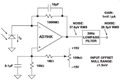
FIG. 4.22: AD795 photodiode preamp with offset null adjustment.

FIG. 4.23: AD795 photodiode circuit performance summary.
The input sensitivity based on a total output voltage noise of 44 µV is obtained by di viding the output voltage noise by the value of the feedback resistor R2. This yields a minimum detectable diode current of 44 fA. If a 12-bit ADC is used to digitize the 10 V full scale output, the weight of the least significant bit (LSB) is 2.5 mV. The output noise level is much less than this.
Photodiode Circuit Tradeoffs
There are many tradeoffs which could be made in the basic photodiode circuit design we have described. More signal bandwidth can be achieved in exchange for a larger output noise level. Reducing the feedback capacitor C2 to 1 pF increases the signal bandwidth to approximately 160 Hz. Further reductions in C2 are not practical be cause the parasitic capacitance is probably in the order of 1 to 2 pF. A small amount of feedback capacitance is also required to maintain stability.
If the circuit is to be operated at higher levels of illumination (greater than approximately 0.3 fc), the value of the feedback resistor can be reduced thereby resulting in further increases in circuit bandwidth and less resistor noise. If gain-ranging is to be used to measure the higher light levels, extreme care must be taken in the design and layout of the additional switching networks to minimize leakage paths.
Compensation of a High Speed Photodiode I/V Converter
A classical I/V converter is shown in FIG. 4.24. Note that it is the same as the photodiode preamplifier if we assume that R1 >> R2. The total input capacitance, C1, is the sum of the diode capacitance and the op amp input capacitance. This is a classical second-order system, and the following guidelines can be applied in order to determine the proper compensation.
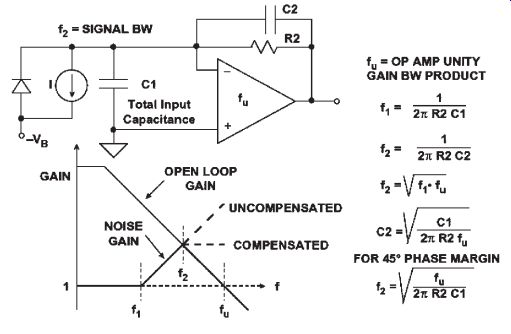
FIG. 4.24: Compensating for input capacitance in a current-to-voltage
converter .
The net input capacitance, C1, forms a zero at a frequency f1 in the noise gain transfer function as shown in the Bode plot.
Eq. 4.3
Note that we are neglecting the effects of the compensation capacitor C2 and are assuming that it is small relative to C1 and will not significantly affect the zero fre quency f1 when it is added to the circuit. In most cases, this approximation yields results which are close enough, considering the other variables in the circuit.
If left uncompensated, the phase shift at the frequency of intersection, f2, will cause instability and oscillation. Introducing a pole at f2 by adding the feedback capacitor C2 stabilizes the circuit and yields a phase margin of about 45 degrees.
Eq. 4.4
Since f2 is the geometric mean of f1 and the unity-gain bandwidth frequency of the op amp, fu, f f fu 2 1 = ·
Eq. 4.5
These equations can be combined and solved for C2:
Eq. 4.6 This value of C2 will yield a phase margin of about 45 degrees. Increasing the capacitor by a factor of 2 increases the phase margin to about 65 degrees.
In practice, the optimum value of C2 should be determined experimentally by varying it slightly to optimize the output pulse response.
Selection of the Op Amp for Wideband Photodiode I/V Converters
The op amp in the high speed photodiode I/V converter should be a wideband FET-in put one in order to minimize the effects of input bias current and allow low values of photocurrents to be detected. In addition, if the equation for the 3 dB bandwidth, f2, is rearranged in terms of fu, R2, and C1, then:
Eq. 4.7
...where C1 is the sum of the diode capacitance, CD, and the op amp input capacitance, CIN. In a high speed application, the diode capacitance will be much smaller than that of the low frequency preamplifier design previously discussed-perhaps as low as a few pF.
By inspection of this equation, it is clear that in order to maximize f2, the FET-input op amp should have both a high unity gain-bandwidth product, fu, and a low input capacitance, CIN. In fact, the ratio of fu to CIN is a good figure-of-merit when evaluating different op amps for this application.
FIG. 4.25 compares a number of FET-input op amps suitable for photodiode preamps. By inspection, the AD823 op amp has the highest ratio of unity gain-bandwidth product to input capacitance, in addition to relatively low input bias current. For these reasons, it was chosen for the wideband photodiode preamp design.
High Speed Photodiode Preamp Design
The HP 5082-4204 PIN Photodiode will be used as an example for our discussion. Its characteristics are given in FIG. 4.26. It is typical of many commercially available PIN photodiodes. As in most high-speed photodiode applications, the diode is operated in the reverse-biased or photo conductive mode. This greatly lowers the diode junction capacitance, but causes a small amount of dark current to flow even when the diode is not illuminated (we will show a circuit which compensates for the dark current error later in the section).
This photodiode is linear with illumination up to approximately 50 to 100 µA of output current. The dynamic range is limited by the total circuit noise and the diode dark current (assuming no dark current compensation).
Using the circuit shown in FIG. 4.27, assume that we wish to have a full scale out put of 10V for a diode current of 100 µA. This determines the value of the feedback resistor R2 to be 10 V/100 µA = 100 k-ohm .
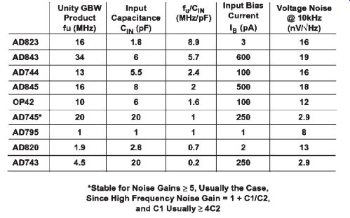
FIG. 4.25: FET-input op amp comparison table for wide bandwidth photodiode
preamps.

FIG. 4.26: HP 5082-4204 photodiode.
[...]
Eq. 4.8
The factor of 1.57 converts the approximate single-pole bandwidth of 2.1 MHz into the equivalent noise bandwidth.
The output noise due to the input voltage noise is obtained by multiplying the noise gain by the voltage noise and integrating the entire function over frequency. This would be tedious if done rigorously, but a few reasonable approximations can be made which greatly simplify the math. Obviously, the low frequency 1/f noise can be neglected in the case of the wideband circuit. The primary source of output noise is due to the high-frequency noise-gain peaking which occurs between f1 and fu. If we simply assume that the output noise is constant over the entire range of frequencies and use the maximum value for AC noise gain [1 + (C1/C2)], then…
Eq. 4.9
The total rms noise referred to the output is then the RSS value of the two components:
Total RTO Noise Vrms = ( ) + ( ) = 73 250 260 2 2 µ
Eq. 4.10
The total output dynamic range can be calculated by dividing the full scale output signal (10 V) by the total output rms noise, 260 µV rms, and converting to dB, yield ing approximately 92 dB.
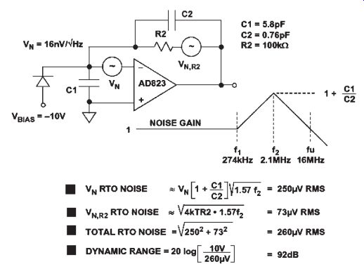
FIG. 4.28: Equivalent circuit for output noise analysis
High Impedance Charge Output Sensors
High impedance transducers such as piezoelectric sensors, hydrophones, and some accelerometers require an amplifier which converts a transfer of charge into a change of voltage. Because of the high DC output impedance of these devices, appropriate buffers are required. The basic circuit for an inverting charge sensitive amplifier is shown in FIG. 4.29. There are basically two types of charge transducers: capacitive and charge-emitting. In a ca pacitive transducer, the voltage across the capacitor (VC) is held constant. The change in capaci tance, ?C, produces a change in charge, ?Q = ?CVC. This charge is transferred to the op amp output as a voltage,
fivOUT = -?Q/C2 = -?CVC/C2.
Charge-emitting transducers produce an output charge, ?Q, and their output capacitance remains constant. This charge would normally produce an open-circuit output voltage at the transducer output equal to ?Q/C. However, since the voltage across the transducer is held constant by the virtual ground of the op amp (R1 is usually small), the charge is transferred to capaci tor C2 producing an output voltage fivOUT = -?Q/C2.
In an actual application, the charge amplifier only responds to AC inputs. The upper cutoff frequency is given by f2 = 1/2pR2C2, and the lower by
f1 = 1/2pR1C1.
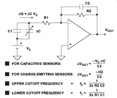
FIG. 4.29: Charge amplifier for capacitive sensor.
Low Noise Charge Amplifier Circuit Configurations
FIG. 4.30 shows two ways to buffer and amplify the output of a charge output transducer. Both require using an amplifier which has a very high input impedance, such as the AD745. The AD745 provides both low voltage and low current noise. This combina tion makes this device particularly suitable in applications requiring very high charge sensitivity, such as capacitive accelerometers and hydrophones.
The first circuit (left) in FIG. 4.30 uses the op amp in the inverting mode. Amplification depends on the principle of conservation of charge at the inverting input of the amplifier. The charge on capacitor CS is transferred to capacitor CF, thus yielding an output voltage of ?Q/CF. The amplifier's input voltage noise will appear at the output amplified by the AC noise gain of the circuit, 1 + CS/CF.
The second circuit (right) shown in FIG. 4.30 is simply a high impedance follower with gain. Here the noise gain (1 + R2/R1) is the same as the gain from the transducer to the output.
Resistor RB, in both circuits, is required as a DC bias current return.
To maximize DC performance over temperature, the source resistances should be balanced on each input of the amplifier. This is represented by the resistor RB shown in FIG. 4.30. For best noise performance, the source capacitance should also be balanced with the capacitor CB. In general, it is good practice to balance the source impedances (both resistive and reactive) as seen by the inputs of a precision low noise BiFET amplifiers such as the AD743/AD745. Balancing the resistive high impedance sensors components will optimize DC performance over temperature because balancing will mitigate the effects of any bias current errors. Balancing the input capacitance will minimize AC response errors due to the amplifier's nonlinear common mode input capacitance, and as shown in FIG. 4.30, noise performance will be optimized. In any FET input amplifier, the current noise of the internal bias circuitry can be coupled to the inputs via the gate-to-source capacitances (20 pF for the AD743 and AD745) and appears as excess input voltage noise. This noise component is correlated at the inputs, so source impedance matching will tend to cancel out its effect. FIG. 4.30 shows the required external components for both inverting and noninverting configurations. For values of CB greater than 300 pF, there is a diminishing impact on noise, and CB can then be simply a large mylar bypass capacitor of 0.01 µF or greater.
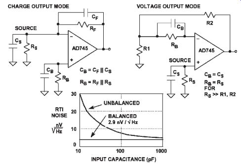
FIG. 4.30: Balancing source impedances minimizes effects of bias currents
and reduces input noise.
A 40dB Gain Piezoelectric Transducer Amplifier Operates on Reduced Supply Voltages for Lower Bias Current
FIG. 4.31 shows a piezoelectric transducer amplifier connected in the voltage- output mode. Reducing the power supplies to +5 V reduces the effects of bias current in two ways: first, by lowering the total power dissipation and, second, by reducing the basic gate-to-junction leakage current. The addition of a clip-on heat sink such as the Aavid #5801 will further limit the internal junction tempera ture rise.
Without the AC coupling capacitor C1, the amplifier will operate over a range of 0°C to +85°C. If the optional AC coupling capacitor C1 is used, the circuit will operate over the entire -55°C to +125°C temperature range, but DC information is lost.
Hydrophones
Interfacing the outputs of highly capacitive transducers such as hydrophones, some accelerometers, and condenser microphones to the outside world presents many design challenges. Previously designers had to use costly hybrid amplifiers consisting of discrete low-noise JFETs in front of conventional op amps to achieve the low levels of voltage and current noise required by these applications. Now, using the AD743 and AD745, designers can achieve almost the same level of performance of the hybrid approach in a monolithic solution.
In sonar applications, a piezo-ceramic cylinder is commonly used as the active element in the hydrophone. A typical cylinder has a nominal capacitance of around 6,000 pF with a series resistance of 10 ohm. The output impedance is typically 108 ohm or 100 M-ohm.
Since the hydrophone signals of interest are inherently AC with wide dynamic range, noise is the overriding concern among sonar system designers. The noise floor of the hydrophone and the hydrophone preamplifier together limit the sensitivity of the system and therefore the overall usefulness of the hydrophone. Typical hydrophone bandwidths are in the 1 kHz to 10 kHz range. The AD743 and AD745 op amps, with their low noise figures of 2.9 nV_/Hz and high input impedance of 10^10 ohm (or 10 G ohm) are ideal for use as hydrophone amplifiers.
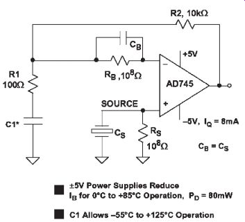
FIG. 4.31: Gain of 100 piezoelectric sensor amplifier.
The AD743 and AD745 are companion amplifiers with different levels of internal compensation. The AD743 is internally compensated for unity gain stability. The AD745, stable for noise gains of five or greater, has a much higher bandwidth and slew rate. This makes the AD745 especially useful as a high-gain preamplifier where it provides both high gain and wide bandwidth. The AD743 and AD745 also operate with extremely low levels of distortion: less than 0.0003% and 0.0002% (at 1 kHz), respectively.
Op Amp Performance: JFET versus Bipolar
The AD743 and AD745 op amps are the first monolithic JFET devices to offer the low input voltage noise comparable to a bipolar op amp without the high input bias currents typically associated with bipolar op amps. FIG. 4.32 shows input voltage noise versus input source resistance of the bias-current compensated OP27 and the JFET-input AD745 op amps. Note that the noise levels of the AD743 and the AD745 are identical. From this figure, it is clear that at high source impedances, the low cur rent noise of the AD745 also provides lower overall noise than a high performance bipolar op amp. It is also important to note that, with the AD745, this noise reduction extends all the way down to low source impedances. At high source impedances, the lower DC current errors of the AD745 also reduce errors due to offset and drift as shown in FIG. 4.32.
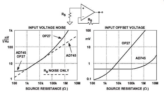
FIG. 4.32: Effects of source resistance on noise and offset voltage
for OP27 (bipolar) and AD745 (BiFET) op amps.
FIG. 4.33: A pH probe buffer amplifier with a gain of 20 using the
AD795 precision BiFET op amp.
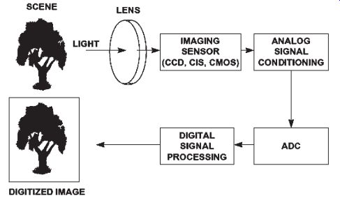
FIG. 4.34: Generic imaging system for scanners or digital cameras.
A PH Probe Buffer Amplifier
A typical pH probe requires a buffer amplifier to isolate its 10^6 to 109 ohm source resis-tance from external circuitry. Such an amplifier is shown in FIG. 4.33. The low input current of the AD795 allows the voltage error produced by the bias current and electrode resistance to be minimal. The use of guard ing, shielding, high insulation resistance standoffs, and other such standard picoamp meth ods used to minimize leakage are all needed to maintain the accuracy of this circuit.
The slope of the pH probe transfer function, 50mV per pH unit at room temperature, has an approximate +3500 ppm/°C temperature coefficient. The buffer shown in FIG. 4.33 provides a gain of 20 and yields an output voltage equal to 1 volt/pH unit. Temperature compensation is provided by resistor RT which is a special tem perature compensation resistor, 1 k-ohm , 1%, +3500 ppm/°C, #PT146 available from Precision Resistor Co., Inc. (Reference 18).
CCD/CIS Image Processing
The charge-coupled-device (CCD) and contact-image-sensor (CIS) are widely used in consumer imaging systems such as scanners and digital cameras. A generic block diagram of an imaging system is shown in FIG. 4.34. The imag ing sensor (CCD, CMOS, or CIS) is exposed to the image or picture much like film is exposed in a camera. After exposure, the out put of the sensor undergoes some analog signal processing and then is digitized by an ADC. The bulk of the actual image processing is performed using fast digital signal processors. At this point, the im-
age can be manipulated in the digital domain to perform such functions as contrast or color enhancement/correction, etc.
The building blocks of a CCD are the individual light sensing elements called pixels (see FIG. 4.35). A single pixel consists of a photo sensitive element, such as a photodiode or photocapacitor, which outputs a charge (electrons) propor tional to the light (photons) that it is exposed to. The charge is accumulated during the exposure or integration time, and then the charge is transferred to the CCD shift register to be sent to the output of the device. The amount of accumulated charge will depend on the light level, the integration time, and the quantum efficiency of the photo sensi tive element. A small amount of charge will accumulate even without light present; this is called dark signal or dark current and must be compensated for during the signal processing.
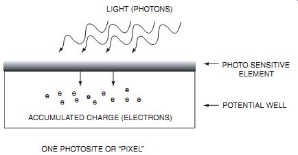
FIG. 4.35: Light sensing element.
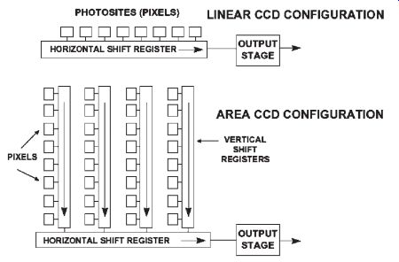
FIG. 4.36: Linear and area CCD arrays.
The pixels can be arranged in a linear or area configuration as shown in FIG. 4.36. Clock signals transfer the charge from the pixels into the analog shift registers, and then more clocks are applied to shift the individual pixel charges to the output stage of the CCD. Scanners generally use the linear configuration, while digital cameras use the area configuration. The analog shift register typically operates at frequencies between 1 and 10 MHz for linear sensors, and 5 to 25 MHz for area sensors.
A typical CCD output stage is shown in FIG. 4.37 along with the associated volt age waveforms. The output stage of the CCD converts the charge of each pixel to a voltage via the sense capacitor, CS. At the start of each pixel period, the voltage on CS is reset to the reference level, VREF causing a reset glitch to occur. The amount of light sensed by each pixel is measured by the difference between the reference and the video level, fiv. CCD charges may be as low as 10 electrons, and a typical CCD out put has a sensitivity of 0.6 µV/electron. Most CCDs have a saturation output voltage of about 500 mV to 1 V for area sensors and 2 V to 4 V for linear sensors. The DC level of the waveform is between 3 to 7V.
Since CCDs are generally fabricated on CMOS processes, they have limited capability to perform on-chip signal conditioning. Therefore the CCD output is generally processed by external conditioning circuits. The nature of the CCD output requires that it be clamped before being digitized by the ADC. In addition, offset and gain functions are generally part of the analog signal processing.
CCD output voltages are small and quite often buried in noise. The largest source of noise is the thermal noise in the resistance of the FET reset switch. This noise may have a typical value of 100 to 300 electrons rms (approximately 60 to 180 mV rms). This noise, called "kT/C" noise, is illustrated in FIG. 4.38. During the reset interval, the storage capacitor CS is connected to VREF via a CMOS switch. The on-resistance of the switch (RON) produces thermal noise given by the well known equation:
Thermal Noise kT BW RON = · · 4
Eq. 4.11
The noise occurs over a finite bandwidth determined by the RON CS time constant.
This bandwidth is then converted into equivalent noise bandwidth by multiplying the single-pole bandwidth by p/2 (1.57):
Noise BW R C R C ON S ON S
Eq. 4.12
Substituting into the formula for the thermal noise, note that the RON factor cancels, and the final expression for the thermal noise becomes:
Thermal Noise kT C
Eq. 4.13
This is somewhat intuitive, because smaller values of RON decrease the thermal noise but increase the noise bandwidth, so only the capacitor value determines the noise.
Note that when the reset switch opens, the kT/C noise is stored on CS and remains constant until the next reset interval. It therefore occurs as a sample-to-sample variation in the CCD output level and is common to both the reset level and the video level for a given pixel period.
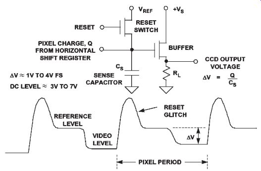
FIG. 4.37: Output stage and waveforms.
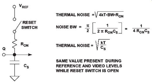
FIG. 4.38: kT/C noise.
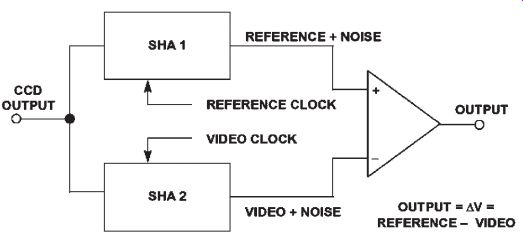
FIG. 4.39: Correlated double sampling (CDS).
A technique called correlated double sampling (CDS) is often used to reduce the effect of this noise. FIG. 4.39 shows one circuit implementation of the CDS scheme, though many other implementations exist. The CCD output drives both SHAs. At the end of the reset interval, SHA1 holds the reset voltage level plus the kT/C noise.
At the end of the video interval, SHA2 holds the video level plus the kT/C noise.
The SHA outputs are applied to a difference amplifier which subtracts one from the other. In this scheme, there is only a short interval during which both SHA outputs are stable, and their difference represents fiv, so the difference amplifier must settle quickly. Note that the final output is simply the difference between the reference level and the video level, fiv, and that the kT/C noise is removed.
Contact image sensors (CIS) are linear sensors often used in facsimile machines and low-end document scanners instead of CCDs. Although a CIS does not offer the same potential image quality as a CCD, it does offer lower cost and a more simplified optical path. The output of a CIS is similar to the CCD output except that it is referenced to or near ground (see FIG. 4.40), eliminating the need for a clamping function.
Furthermore, the CIS output does not contain correlated reset noise within each pixel period, eliminating the need for a CDS function. Typical CIS output voltages range from a few hundred mV to about 1 V full scale. Note that although a clamp and CDS is not required, the CIS waveform must be sampled by a sample-and-hold before digitization.
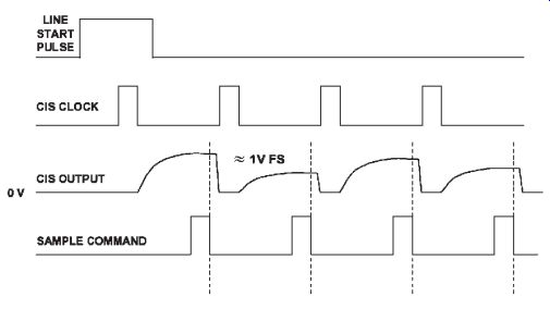
FIG. 4.40: Contact image sensor (CIS) waveforms.
Analog Devices offers several analog-front-end (AFE) integrated solutions for the scanner, digital camera, and camcorder markets. They all comprise the signal processing steps described above. Advances in process technology and circuit topologies have made this level of integration possible in foundry CMOS without sacrificing performance. By combining successful ADC architectures with high performance CMOS analog circuitry, it is possible to design complete low cost CCD/CIS signal processing ICs.
The AD9816 integrates an analog-front-end (AFE) that integrates a 12-bit, 6 MSPS ADC with the analog circuitry needed for three-channel (RGB) image processing and sampling (see FIG. 4.41). The AD9816 can be programmed through a serial interface, and includes offset and gain adjustments that gives users the flexibility to perform all the signal processing necessary for applications such as mid- to high-end desktop scanners, digital still cameras, medical x-rays, security cameras, and any instrumentation applications that must "read" images from CIS or CCD sensors.
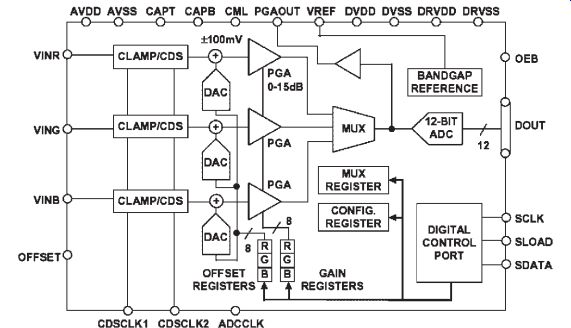
FIG. 4.41: AD9816 Analog front end CCD/CIS processor.

FIG. 4.42: AD9816 key specifications.
The signal chain of the AD9816 consists of an input clamp, correlated double sampler (CDS), offset adjust DAC, programmable gain amplifier (PGA), and the 12-bit ADC core with serial interfacing to the external DSP. The CDS and clamp functions can be disabled for CIS applications.
The AD9814, takes the level of performance a step higher. For the most demanding applications, the AD9814 offers the same basic functionality as the AD9816 but with 14-bit performance. As with the AD9816, the signal path includes three input channels, each with input clamping, CDS, offset adjustment, and programmable gain.
The three channels are multiplexed into a high performance 14-bit 6 MSPS ADC. High-end document and film scanners can benefit from the AD9814's combination of performance and integration.
NEXT: Acceleration, Shock and Vibration Sensors
PREV: part b