by Dr. Norman E. Thagard
[[Norman E. Thagard, M.D., is a NASA astronaut who has been selected as a prime crew member for a 3-month flight on the Russian space station Mir this spring. ]]
Continuing this article on building high-end Class-A amplifier (100 watt, into 8 ohms, 0.1 %) or less TIM], l will describe the power supply and output stage part I covered the low-level stages and story and philosophy behind the design.
Power Supply
Nelson Pass, a designer of high-end audio equipment who helped me with this amplifier, was concerned that the local feedback scheme might inject noise into the amplifier. He indicated that this objection would he removed if the driver stage were operated from a separate regulated supply. This was good news, because the intent from the beginning was to do this, albeit for another reason: The MOS-FETs used here are all enhancement-mode devices, which means that a gate-to-source voltage of 5 V or so is required to saturate them. If the driver stage were operated from the same supply as the output, the-output swing could never be closer than 5V to the output-rail voltage, which would significantly reduce the amplifier's rated power output. This is even more onerous for a class-A amp, where the already high quiescent power dissipation would be unnecessarily raised and cause even greater inefficiencies.
The 55-V driver rails allow the output to swing almost the whole 100-V (+50 to-50 V) output power-supply differential. All of my amplifier designs have used half-wave voltage doublers, followed by voltage regulators, to power the front-ends. Such doublers have limited current' capability, but amplifier front-ends have current-requirements well within that capability. The alternative to the doubler would be an independent supply requiring either a separate power transformer or additional windings on the main power transformer. In my experience, the single transformers with the desired additional windings are impossible to come by, and it is difficult to physically locate a second power transformer in the usual cramped chassis.
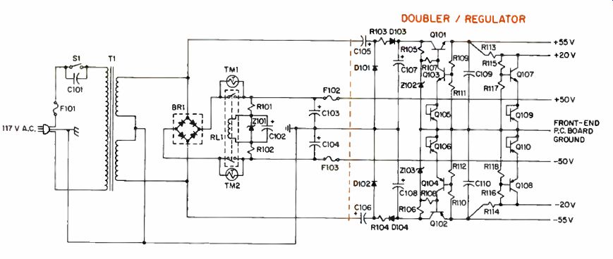
FIG. 2--Power-supply schematic.
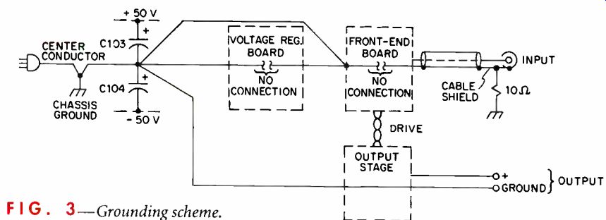
FIG. 3--Grounding scheme.
The emphasis of this article is on the signal circuitry. Even so, I would be remiss to ignore the design of the voltage doubler/regulators. I use from my 30-year-old electrical engineering text for the doubler design. A description of the positive supplies follows; the negative supplies perform similarly, as can be inferred from Fig. 2.
Initially, C105 will charge through D101 to a level approaching the a.c. peak voltage of the power transformer's secondary, i.e., about 50 V. The D101 anode voltage will drop below cathode voltage as the cycle continues, cutting off D101 and preventing C105 from discharging through that diode.
During the next cycle, the positive terminal of C105 will approach 100 V, as its negative terminal will rise to the transformer secondary voltage (remember, the voltage across a capacitor cannot change instantaneously, and C105 was previously charged to 50 V). Because the required voltage rating of C105 is thus seen to be at least 50 V, use a 63-V capacitor. Capacitor C107 will charge through R103/D103 to a level less than twice the peak secondary voltage. Resistor R103 will lessen the charging current pulse amplitude, which will make the voltage at the doubler output (D103/C107 junction) somewhat less than it would otherwise be. You can increase R103 at the expense of that voltage, but the doubler out put voltage needs to be 85 V or more to ensure proper operation of zener Z102. I you measure less than 85 V here, reduce the value of R103. Clearly, C107 needs to have a voltage rating significantly greater than 85 V.
The R105/Z102/R107 scheme is some times called preregulation. Its use should improve performance of the downstream regulators. A simple discrete series voltage regulator is formed by Q101/Q103, for which Q105 is a stable 7-V reference. Out put voltage is set by the formula:
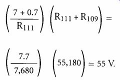
The 0.7 V in the formula is the Vbe for Q103.
The 55-V regulated output is then further regulated down to 20 V by a simple, discrete shunt regulator. This regulator behaves somewhat like a zener in that it will conduct whatever current is required to maintain 20 V at the output. Thus, the function of R113 is to limit that current so that regulator component limitations will not be exceeded. Too high a value for R113 will cause the output to drop below 20 V.
Transistor Q107 is the shunt, while Q109 is a 7-V reference. Output voltage is determined from the formula:
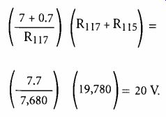
Here, The 0.7 V of the formula is the Vbe of Q107.
Seven-volt zeners can be substituted for transistors Q105, Q106, Q109, and Q110.
Precision 5-V references are also available, but their use will require changes in the resistor values to give correct voltages for regulator output.
Other Circuitry
The grounding scheme (Fig. 3) is worth a quick comment. The star ground technique, in which a single ground point exists, is employed; all system grounds are re turned to this point. I used heavy gauge brass bus bars to connect the ground terminals of the main power-supply electrolytic capacitors, C103 and C104. This is the system ground. The ground trace on the doubler/regulator p.c. board is intentionally broken, that is, the board's input ground is not continuous with its output ground. Instead, the wire lead from the output ground trace goes directly to the front-end's p.c. board ground connection and from there is routed back to the system ground point. This part of the grounding scheme keeps voltage spikes from the half-wave doubler out of the ground bus for the regulators, which results in a cleaner regulated supply rail.
To prevent ground loops, the signal in put ground is not continuous with the front-end's p.c. board ground discussed in the preceding paragraph. Instead, only the input components C2/R2 and the feedback resistor R34 have their grounds connected to the ground terminal of the input RCA jack. The jack's ground terminal is connected to the chassis through a 10-ohm resistor. The chassis itself is connected to the system ground from one point only, with a heavy gauge wire. I have used well-shielded audio cable to connect the RCA jack to the front-end's p.c. board, but this is probably not required.
But I digress, and shall now return to the circuit description. The output MOS-FETs do require biasing for linear operation, so Q21 is at the heart of a variable voltage source that provides the 10 or 11 V from the p- to the n-channel gate. Used as a V, multiplier, Q21 has a collector-to-emitter voltage adjustable by trimpot P2. While a potentiometer could be used directly to provide the gate-spreading voltage, it is not prudent to run much current through one.
Therefore, the circuit here-the one used in all but the simplest amplifiers-is de signed to give some protection against in advertent high biases or failures that might fully turn on the output transistors. This arrangement should be a d.c. voltage source and an a.c. short. Capacitor C7 offers some noise suppression and lowers a.c. impedance at higher frequencies.
I mentioned in Part I that no global feedback is used. That is true for the complete amplifier, but the front-end does in corporate feedback from driver to input.
Driver output is sampled and fed back to the input via R31 through R34. The closed loop gain is set by the ratio:
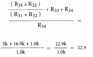
and is about 20. This sets the amplifier's sensitivity to a fairly typical value. Capacitor C8 is another form of compensation and was used here to shape the square-wave response [5]. The value of 5 pF gave a very slightly overdamped response, which looks very good on an oscilloscope.
OUTPUT STAGE
In the output stage, Z3/D4 and Z4/D5 form a protection network to safeguard the gates of Q24 through Q35 from damaging overvoltages. With the use of global feed back, a reactive load that lags the output will cause drive voltage to increase as the feedback loop attempts to force the output to follow the (amplified) version of the in put. This can easily produce gate-to-source voltages which imperil the output MOS FETs. While this open-loop amplifier will have no such tendency, it is still wise to in corporate this inexpensive protective net work to avoid the cost and trouble of re placing the MOS-FETs.
Transistors Q22 and Q23 are constant-current sources. Without them, bipolar power transistors Q36 through Q47 would run out of base-current drive as the output voltage approached the supply rails. This, then, is another case where the amp's power rating would be unnecessarily limited if appropriate countermeasures were not taken. As a rule of thumb, I use a bias current that is about 10% of the output bias cur rent, which is almost always sufficient to fully drive the output while not so excessive as to place unreasonable burdens on Q22 and Q23. Since R37 and R38 are 3.9-ohm resistors, bias current is 0.23 ampere (0.9 divided by 3.9), which is about 10% of the 2.5-amp output bias. (The 0.9 in the equation is, of course, the voltage drop across the series diodes D6 and D7, which is about 1.5 V, less the 0.6-V Vbe of Q22.) Since the 0.23 ampere flows through R66 (R67), base voltage of the output bipolars is 6.2 V (0.23 times 27), which means a little less than 5.6 V (6.2 minus 0.6) is across the output MOS-FET channels. This is another advantage of cascoding: Devices with lower power and voltage ratings may be used in a critical application. These MOS FETs are responsible for the thermal behavior of the output, and cascoding them improves performance since they dissipate far less power than if they had the entire supply voltage across them.
The most important consideration for a Class-A power-output stage at this power level is its thermal stability. If biased by a constant-voltage source, a bipolar transistor will exhibit a negative thermal coefficient. Some authors choose to call this a positive coefficient. I use the convention in the International Rectifier MOS-FET Data Book, which refers to the effective resistance of the device. As it heats up, the effective resistance of the channel decreases, which results in more current, which results in more heat, and so on. Self-destruction can be the outcome. The output in this design is biased by a constant-voltage source, namely the Vbe multiplier, Q21. However, no tendency to thermal runaway occurs, because it is the MOS-FETs, not the bipolars, which are so biased.
Now, in spite of what you may have heard about positive thermal coefficients of MOS-FETs, in a linear application such as this, MOS-FETs will also conduct a little more current as they warm up. This hap pens because the positive thermal coefficient of the channel is more than offset by the thermal behavior of the gate-to-source voltage [6]. For a given drain current, the required Vg5 drops with increasing temperature. At the high drain currents seen in switching applications, the channel characteristics predominate and the often touted thermal advantages of MOS-FETs do, in deed, exist.
There is no need for alarm. Even in the present application, this increase in drain current with increasing temperature is self-limited, so that thermal runaway will not occur. As a matter of fact, Q21, which is a medium-power bipolar transistor, will experience a drop in its V, as it warms up.
Since it functions as a V multiplier, out put MOS-FET bias will drop. The overall thermal characteristic of this amplifier is the desirable one, that is, output bias will tend to fall somewhat as it warms up. Obviously, then, Q21 should be mounted on a heat-sink. Even though a heat-sink is not required for its modest power dissipation, it is required to keep the output bias from sagging excessively. (Otherwise, this Class-A amp will degrade to high-bias AB as it warms up.)
I did not match either the MOS-FET or the bipolar output transistors. Nonetheless it is important that the MOS-FETs be reasonably well matched, or they will not equally share the output bias current. For the reason given above, inequalities in cur rent sharing will actually be aggravated as the MOS-FETs warm up. Source-degeneration resistors R52 through R63 will improve the current sharing and improve output linearity; they could be increased to 1 ohm at the expense of lowering damping factor. With carefully matched MOS-FETs, these resistors could also be eliminated, but I like to use them because it would other wise be difficult to determine the performance of a particular leg of the paralleled output. MOS-FETs from the same lot would likely be adequately matched. Purchasing all of the MOS-FETs from the same vendor at the same time usually gives you transistors from the same lot, which was certainly my experience with this amplifier.
The 250-watt bipolar output devices have no choice but to conduct whatever current their cascode partner sends them, so matching the bipolars is unnecessary.
Since power output = (rms current) 2 x load impedance, then the rms current = sqr-rt(power/8) = √(100/8)= 3.5 amperes. Peak current = rms current x √2 = 3.5 x 1.4 = 5 amperes. At 100 watts, current will vary from near zero up to the peak of 5 amperes. For Class-A operation, the current must never go to zero (output devices must conduct throughout the cycle), so the out put bias must be set to at least 2.5 amperes.
Paralleled MOS-FETs can self-oscillate due to parasitic device reactances. Gate resistors R40 through R51 should prevent such oscillations. Not enough is said about oscillations in power amplifiers; even some commercial amps have had such problems.
This was my third scratch-built amplifier, and all three initially had oscillations. (Let me add that the first two scratch-built amps that oscillated were not of my de sign.) Stray coupling can be the culprit.
Keeping input separated from output can help with this, as can ground-plane construction of p.c. boards and grounding heat-sinks (I have seen stray coupling to transistors mounted to ungrounded heat sinks). I routinely do these things, as is evidenced in this design. Inadequate bypassing of power-supply runs can cause problems, since the power supply should ideally be an a.c. short circuit. There can be enough inductance in the wire carrying power from the supply to the p.c. board to cause onboard problems. Thus, the front end board in this design allows for power supply bypassing. Although keeping lead lengths short is desirable, a 100-watt Class A amplifier has massive heat-sinks, so it is impossible to keep all lead lengths short.
The prototypes were built with no concern for layout other than a reasonable separation between the input and output portions of the circuit. Nonetheless, the amplifier has no detectable oscillations; the open-loop topology no doubt contributes to this stability. No series output inductor, of the kind frequently used in power amplifiers to isolate the output from reactive loads, is needed, and the amp has driven capacitive loads with no apparent problems. In this regard, it is an excellent project for those who would like to have assurance that the outcome of their efforts will be successful.
The RC output filter formed by C13/R39 is ubiquitous in power amps. Although I detect no difference in bench tests of performance with or without the filter, Pass assures me there is a load lurking out there that will require it. The values used for C13/R39 are the most typical.
Diodes D10 and D11 protect the amplifier output from reactive loads which could induce EMFs high enough to reverse the polarity across the output transistors. This could even happen with lower EMFs in this Class-A amplifier, because rail voltage falls rapidly at power off. A reactive load could hold the output well above virtual ground, leading to the polarity reversal. The diodes clamp the output voltage to a magnitude no greater than one diode drop above the rail voltage.
Fuse F1 protects the amplifier from in advertent output shorts and the load from amplifier failures or problems in signal sources connected to the amp. All amplifiers have failure modes that can result in the output heading straight to the supply rails. To deliver 100 watts into an 8-ohm load, F1 must be rated at 4 amperes or more. In Pass' experience, fuses smaller than 6 amperes sometimes have adverse auditory effects. A 6-ampere fuse may or may not blow if a fault occurs, thus placing the amplifier or its load at risk. You must be the judge of the efficacy of F1.
Some argue that output fuses lower an amplifier's damping factor. Indeed, output fuses can do so, because they increase the output impedance by the amount of their own impedance. In a feedback amplifier, the fuse impedance can be the major contributor to output impedance. That is less likely in this open-loop amplifier, since output impedance is inherently higher. (Feedback has several effects; in addition to lowering THD, it also reduces output impedance by the amount of the feedback).
In the rush to extremely high damping factors, the already low absolute value of the output impedance is often overlooked. Of more importance, I think, is the frequency dependence of the damping factor. I measured 45 at 1 kHz, 40 at 10 kHz, and greater than 35 at 20 kHz. Since damping factor is the ratio of load impedance to amp output impedance, the output impedance for the standard 8-ohm load at 20 kHz is 0.23 ohm (8 divided by 35). Looking at this from another perspective, we are less than 0.25 ohm from a perfect voltage source, which is the ideal.
A few words are due concerning the main power supply. If rated output is to be realized, the rail voltage must drop no lower than 46 V in operation. The current required from the supply will be around 3 amperes at that voltage. Rounding off yields a power dissipation of 300 watts. The power transformer, T1, must be capable of providing this kind of power, and a good rule of thumb would be a VA rating of about twice the 300 watts. Since the 300 watts is somewhat conservative, a 500-watt transformer is probably adequate if the amplifier is properly ventilated. A toroid is preferred but not essential.
There is no need to regulate the main power supply, but it must be adequately filtered. I recommend that filter capacitors C103 and C104 be at least 15,000 µF. Their voltage rating should be at least 63 V.
Large filter capacitors will result in welded contacts unless the power switch has a very high current rating or in-rush current limiting is provided. The relay/thermistor arrangement of RL1, TM1, and TM2 used here works well. At power on, the filter capacitors look like a short circuit. The transformer/rectifier doesn't see this short, because the 10-ohm cold resistance of the thermistors is interposed. As the filter capacitors charge toward the 50-V level, the pull-in voltage of the relay is finally reached, which bypasses supply current around the thermistors. There is always a chance that the relay contacts would not close. Even if such a failure occurs, no hazard exists since the thermistors are rated to carry the full supply current. There would be an increase in power-supply output impedance by the amount of the hot resistance of the thermistors, but this is less than 1 ohm.
The final installment of this article will cover construction methods and will include a complete Parts List plus circuit-board patterns and board-stuffing diagrams.
REFERENCES
1. Leach, Marshall, "Build a Low TIM Amplifier," Audio, February 1976 ("Addendum," April 1976, pg. 12).
2. Pass, Nelson, "Cascode Amp De sign," Audio, March 1978.
3. Yunik, Maurice, Design of Modern Transistor Circuits, Prentice-Hall, 1973 (pp. 144 to 147).
4. Joyce, M. V. and K. K. Clarke, Transistor Circuit Analysis, Addison-Wesley, 1961 (pp. 98 to 101).
5. Rosenstark, Sol, Feedback Amplifier Principles, Macmillan, 1986 (pp. 112 to 118).
6. "Paralleling MOSFETs in the Linear Mode," Power MOSFET Transistor Data, Motorola, 1985 (pp. A63 to A65).
===================
(adapted from Audio magazine, Feb. 1995)
= = = =
Also see: