Authors: Walter G. Jung, Mark L. Stephens, and Craig C. Todd
------
Portions of this article are adapted from "Slewing Induced Distortion in Audio Amplifiers" by the authors in The Audio Amateur, Feb., 1977 ( P.O. Box 176, Peterborough, N.H. 03458), part of an article series which is available in book form. Portions were also adapted from the authors' article "Slewing Induced Distortion Its Effect on Audio Amplifier Performance, with Correlated Listening Results," Audio Engineering Society Preprint No. 1252 from the May, 1977, convention. (See bibliography references nos. 33 and 34.) ©Copyright 1979 by Walter G. Jung, Mark L. Stephens, and Craig C. Todd.
------
Calculation of Slew Induced Distortion
Thus far, little has been said in the literature about how to calculate slew induced or transient intermodulation distortion. This is, no doubt, due to the complexity of the problem, especially handling the frequency dependence of the amplifier stages and the incorporation of feedback. There is, however, a straightforward technique that can be used to find closed-form expressions for every possible harmonic or intermodulation distortion component. The technique involves forming a Volterra series to characterize the output as a function of some input variable [57]. The coefficients of the Volterra series can then be used to find the magnitude and phase of all distortion products. This technique has been widely used to predict distortion in radio frequency circuits with a high degree of accuracy.
Unfortunately, it takes more time and space to explain the technique itself than it does its application to a given problem. For this reason, we have not included a full analysis within the article and direct the interested reader to the reference cited. However, with appropriate assumptions and simplifications, many useful features of the Volterra series technique can be used to find approximate expressions for SID. These are conceptually easier to understand and are quite accurate for relatively small distortion conditions.
Consider a 741-type operational amplifier, which can be broken down into two basic stages, an input trans conductance amplifier and an integrating amplifier. These are shown in Fig. 27. The transconductance stage is assumed to be the dominant nonlinearity and consists of a symmetrical saturating-type characteristic which is independent of frequency. The nonlinear characteristic (formed by a double differential pair) is modeled as a current source output Ai, fo an input differential voltage AV, and can be represented by

(21)
where VT = KT/q or approximately 26 mV at 300° K and IK = the bias current of the stage.
The graph of equation (21) is shown in Fig. 28.
Equation 21 and Fig. 28 differ from equation 13 and Fig. 6b in our previous example of Part I, because the 741 input stage has a pair of transistors on each side. Equation (21) in its present form will not allow closed form expressions for distortion.
It must be expressed as a truncated power series with variable AV to complete the calculations, and this is shown in equation (22).

(22), (23)
The first term in the power series is the desired linear component, and the cubic term (and other higher order terms)
form undesirable distortion products. Distortion will eventually be calculated from (23) after making some additional necessary assumptions.
The second stage in the 741, the integrator, is assumed to be ideal and has a gain characteristic G(f) which is proportional to 1/f. This is expressed by
G (f) = K2/f. (24)
There is a Tr/2 phase shift in (24) which has been neglected.
The reason for this will become evident as the calculation progresses.
The constant K2 is determined by the overall gain of the composite amplifier, which must be approximately unity at a frequency of 1 MHz to make our circuit model represent the performance of a real 741-type op amp.
The actual gain characteristic of a 741 op amp is summarized by the Bode plot in Fig. 29. For most audio-frequency calculations, it is convenient to neglect the low frequency pole at 10 Hz and to assume infinite d.c. gain and a constant, gain-bandwidth product. This has a negligible effect on calculations, since it will be shown that the distortion is determined by the available loop gain at high frequencies.
The open loop gain for this approximation is specified by

(25)
By combining equations (23), (24) and (25), the constant K2 can be expressed in more familiar terms. At a frequency of 1 MHz we have:

(26), (27), (28)
The 741-type op amp that has been developed thus far is now placed in an inverting gain configuration with resistive feedback components. The feedback network is assumed to be linear and independent of frequency. The circuit used for distortion calculations is modeled in Fig. 30. In this circuit, a feedback factor ß can be specified as a function of R1 and R2

For inverting gains of 1, 10, and 100 the factor ß is 1/2, 1/11 and 1/101, respectively.
Additional assumptions that must be made to simplify calculations are:
1) Small distortion conditions exist (<1%). This enables a power series expansion of the trans conductance nonlinearity.
2) The distortion consists of only odd-order products because of symmetry, and, because of 1), the distortion is dominated by third-order terms.
3) The distortion is reduced by the magnitude of the factor (1 + loop gain), at the frequency of the distortion product. It is further assumed that loop gain is much greater than 1, so that distortion is reduced by approximately the magnitude of the loop gain. Any phase shift in the loop gain can therefore be neglected.
A harmonic distortion analysis will be developed here to compare with measured data, although an intermodulation analysis could also have been pursued. The final result will solve for harmonic distortion (which is dominated by the third harmonic) as a function of output voltage level, frequency, and feedback factor (or closed loop gain). The following method will be used to solve for harmonic distortion. First, an output level Vo and frequency f will be specified. Then using (25), AV will be calculated and used in (23) to find open-loop distortion. Finally the loop gain will be computed and used to predict the closed-loop distortion.
For a sinusoidal output voltage of Vo cos 2rrft, we can compute delta V from (25)

(31)
If this AV is substituted into (23) and simplified, the resulting equation will show an open-loop distortion ratio of:

(32)

Fig. 27 Two-stage model of an op amp.

Fig. 28 Transfer characteristics of a transconductance amplifier.

Fig. 29 Gain-frequency characteristics for a 741 op amp.

Fig. 30 Model amplifier with feedback applied.
The open-loop distortion is reduced by the loop gain at the third harmonic frequency, 3f, and by the integrator frequency response which attenuates the third harmonic by a factor of 3.
The loop gain at frequency 3f is

(33)

Fig. 31 Calculated and measured distortion vs. frequency for a 741 at a
gain of -1.

Fig. 32 Calculated and measured distortion vs. frequency for a 741 at a
gain of-10.
Therefore the closed loop distortion is:

(34)
(35)
Equation (35) shows that harmonic distortion should vary directly with the cube of the input frequency, directly with the square of output voltage, and inversely with the feedback factor, ß. In order to test the accuracy of this equation, calculated data for distortion was compared directly with measured THD data from a 741 amplifier. Figures 31, 32 and 33 compare calculated and measured distortion for a constant-amplitude, swept-frequency test condition for three values of feedback factor, ß. Figure 34 compares calculated and measured distortion for a constant-frequency, swept amplitude test condition, also for three values of feedback factor. The agreement is generally good and is excellent for the swept frequency tests. At lower distortion levels, the agreement deteriorates due to the noise floor of the distortion analyzer.
At higher distortion levels, the agreement deteriorates due to large distortion conditions, that is, the fundamental assumptions in developing the calculation are violated. The anomalous behavior of the G = 100 test results is due to the loop gain falling below unity at 10 kHz, which also violates a basic assumption of the calculation. Figure 34 indicates an additional crossover type of distortion that dominates at low signal levels and masks the true distortion characteristics. It should be clear from all the figures that increasing feedback reduces distortion.
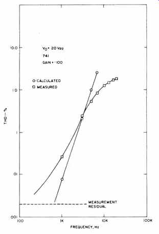
Fig. 33 Calculated and measured distortion vs. frequency for a 741 at a
gain of -100.
Equation (35) was developed specifically for the 741 op amp, which has a unity gain frequency (fT) equal to approximately 1 MHz and a differential input stage consisting of four bipolar devices. A more generalized equation can also be developed which allows fT to be a variable and which permits the number of input devices (n) to vary. This equation is

[36]
where n = number of bipolar devices (2, 4, 6, ...), VT = KT/q = 26 mV at 300° K, ß = feedback factor, fT = unity gain frequency, Vo = output voltage, and f = frequency of fundamental.
Equation (36) reveals some characteristics of SID which were not evident from equation (35). First, it can be seen that increasing n reduces the distortion. This is due to a reduction in the curvature of the input transconductance curve (i.e. less change in gm for the same current change) as n increases.
Unfortunately, practical limitations usually require n to be 2 or 4 at most, so increasing n has a limited usefulness in reducing SID. Second, equation (36) shows the strong effect of the unity gain frequency on SID. Increasing fT by a factor of 3 results in a distortion reduction of almost 30 dB! Clearly, fT is a highly important parameter in improving SID. However, it is important to make the close connection between fT and the SR limit. As pointed out by Solomon [21, 24] and others, for the 741-type circuit topology with bipolar input devices, fT is proportional to the SR limit. This relationship is shown below

(37)
Therefore, improving fT produces a proportionate improvement in the SR limit, which reduces SID.
Results of SID Calculation And Comparison with Measurements
The demonstrated accuracy of (35) and the generalized form in (36) in predicting harmonic distortion in a 741 amplifier leads to some useful conclusions concerning slew induced distortion.
1) It means that slew induced distortion can be modeled and calculated with closed-form expressions, based on Volterra series principles.
2) It shows that slew induced distortion is increased by the input signal slope (SS) and the sharpness of the transconductance curve. It also shows that SID is decreased by more feedback and by a higher gain-bandwidth product.
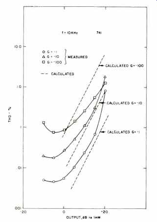
Fig. 34 Distortion vs. output level for a 741 at various gain levels.

Fig. 35 Distortion vs. frequency for a 741 at various feedback conditions.

Fig. 36 Transient intermodulation distortion vs. slew rate ratio for a 4558,
operated inverting at two gain levels.
3) It demonstrates that since the slope of a constant amplitude sine wave is proportional to its frequency, that SID (or DIM, as in the sine-square test) should vary as the cube of the input SS. This is confirmed by the data in Figs. 20 and 24 that show the variation of DIM with SS is a cubic relationship.
4) It shows that increasing a device's slew capability, without adding additional nonlinearities (like slew enhancement), will reduce slew induced distortion.
The Effect of Feedback for SS>SR
Present TIM theory suggests that feedback increases distortion. Our measurements and calculations show that, at least for signal conditions below the slew rate limit (SR ratio <1), that feedback reduces distortion. The overall effect of feedback on distortion (for a constant slew rate capability) is shown by our data to depend on whether the SS is less than or greater than the SR limit. For SS<SR, increasing feedback reduces distortion. For SS>SR, increasing feedback increases distortion. There is a crossover point around SS=SR where feedback has a minor effect on distortion. These trends are evident in the THD plot of Fig. 35 and the sine-square (TIM) plot of Fig. 36. It should be remembered, however, that for distortion-free performance the SS must be less than the SR, and if this criterion is met, feedback can generally be relied on for distortion reduction. Operating an amplifier with the SS>SR is simply not a realistic consideration for high-fidelity reproduction. Some discussion and experiments of the next section will clarify these points further.
Designing for Minimal SID or TIM
We have now reached a point where the factors which govern the behavior of the SID mechanism have been discussed in principle. However, the discussion thus far has been largely focused on behavior as viewed from outside an amplifier or how to characterize it in terms of SID. Perhaps more important is how to design an amplifier from the ground up for minimum susceptibility to SID or TIM. This section focuses on these aspects of the situation and develops techniques which can be used to predictably model circuit performance.
We will begin the discussion by returning to a two-stage amplifier model, shown in Fig. 37, which is similar in many regards to Fig. 5a of Part I or to Fig. 27 above. This two-stage circuit will now be used to develop a general topology which can be used to model amplifier performance and also dramatically illustrate the TIM and SID phenomenon.
A circuit topology similar to Fig. 37 was described 10 years ago in a classic paper by Solomon [24] et al. This paper contained a number of defining behavioral relations, which are not only historically important, but are also applicable to amplifiers of this type in general [47, 64]. A basic point which should be appreciated with regard to this two-stage amplifier is that one can actually design it to yield a given overall gain-bandwidth for an infinite set of combinations of stage 1 and stage 2 gains. The key question is, does it matter whether stage 1 or stage 2 furnishes the bulk of the gain? For herein lies the answer to the entire TIM and SID problem. In other words, how should the gain be partitioned between the two stages for best overall performance? Before we plunge into the equations which govern this, perhaps some discussion would be helpful towards insight.
We have already established by (14) that the SR which will be seen at Vo is set by I K and Cl. However, we also know that to increase SR we cannot just arbitrarily increase IK or decrease Cl, because of stability reasons. We must also decrease gm simultaneously with either of these measures to maintain stability. In general, a lower gm implies less gain in stage 1, i.e. the stage can accept greater input error signals AV before the saturation which results in TIM and/or SID is reached. Thus, it can be said that to maximize SR in a given bandwidth, the stage preceding the integrator of a two-stage amplifier design such as this must have a low gm and high IK. Solomon expressed this as a lowgm/Ik ratio in [24] and [21], and it has also been expressed as a highlk/gm ratio by Gray and Meyer in [22]. The latter form allows an expression to be written which directly describes the amplifier's maximum input-voltage capability or dynamic range. This is the voltage which, when exceeded, will result in slewing. It is simply
(38)
Others have termed this the input-voltage dynamic range [50]; however, the meaning is similar.
A greater application for how these relationships function may be obtained by examining two representative IC amplifiers with dissimilar Vth's. These types are used as examples because they are externally compensated and readily available. This allows convenient experimental duplication. A 301A amplifier (or 741, as noted above) has a gm of
(39)
This equation can be expressed in terms of
(40)
Since VT = 26 mV at room temperature, a useful approximation of (40) is

(41)
Thus, a peak input voltage of 104 mV to a 301A (or 741) will cause it to slew.
To turn to another amplifier type, a representative FET input device is the TL070 (or TL080) which has a gm of approximately

(42)
If this relation is expressed in terms of Vth, it becomes

(43)
As can be noted by comparison of (41) and (43), the TL070 FET achieves a Vth more than six times that of the 301A bipolar for similar conditions, This, for a comparable bandwidth, produces a higher SR. For example, for a 1 MHz bandwidth condition, the TL070 has a 4.3 V/ pS SR (Cc = 47 pF), while the 301A is only 0.67 V/ pS (Cc = 30 pF) [31].
For the amplifier model under discussion, a relationship can also be drawn between Vth, SR, and gain-bandwidth product (GBP) similar to that expressed in [24]. We use the more general GBP, rather than fT, since GBP can often exceed fT. Also, fT is usually taken to mean the unity-gain crossover frequency and implies unity-gain stability. This is not always a requisite. An expression for SR in these terms is

(44)
where SR is in V/ NS, Vth in volts, and GPB is the gain bandwidth product (Hz) at audio frequencies. (The relevance of this equation to the subject of TIM and SID is fundamental. Although first described by Solomon and others [24], the authors would like to document that this relationship's importance to audio amplifier performance has been previously noted in letters to the A.E.S. by R. Cordell of Bell Labs, 9/77, and B. Olsson of Xelex AB, 11/77 and 2/79.) This relationship clearly demonstrates that SR is directly proportional to Vth and GBP for this model. However, the caution should be extended that it does not apply universally. Two particular exceptions are some feed-forward amplifiers and slew-enhanced circuits such as IC type 531. In the case of a feed-forward type, such as the 5534, Vth is not altogether a straightforward predictor of SR, as its Vth of 52mV and fT = 10 MHz predicts only a 3 V/ pS SR. However, the GBP of this device is actually 22 MHz at audio frequencies if this figure is used in (44), the SR predicted is 7 V/ NS, which agrees reasonably well. An important point is also that one must not be misled into the belief that slew-enhanced devices, which can show large voltages for Vth, lead directly to quality results. As has been shown previously, such amplifiers must be treated individually, as their dynamic input nonlinearities makes them special cases.
The relationship described by (44), while certainly an important one, can be erroneously misinterpreted. For example, it should not be interpreted to mean that only a very high Vth is fundamentally the route to high SR and thus low TIM. As (44) clearly shows, raising GBP (where allowable) achieves a similar result, and a practical example is the amplifier compensated for a higher noise gain (and thus GBP), such as the 301A of Fig. 11 (Part II). Such an example illustrates a low Vth device (the 301A) achieving a high SR. Another example is the 5534, a high GBP device, but with a very low Vth, only 52 mV! And, it should be noted, sufficient GBP must be present to result in a useful final closed-loop bandwidth.
The important thing to be remembered for this relationship is not totally Vth or GBP in absolute terms, but their interrelationship, which in many cases can be manipulated to achieve a high SR. The concept of a high Vth is, of course, most important when one is attempting to maximize SR with a given GBP, for as (44) shows, it is the only way it can be done with this type of circuit topology.
Experiments Which Demonstrate The Principle
A very cogent demonstration of the just described relationships can be made by synthesizing a two-stage amplifier model and subjecting it to various feedback and open-loop performance combination.
The circuit used for a series of these experiments is shown in Fig. 38 and is actually composed of two local-feedback IC op amps, which together comprise the model. Al performs the function of a gm input stage, converting the input voltage

Fig. 37 Two-stage transconductance-integrator model of a practical amplifier.

Fig. 38-Synthesized two-stage amplifier model.

Fig. 39 Test circuit for synthesized model.

Fig. 40-THD vs. frequency of the synthesized 741 op-amp model for various
rate slew conditions (Test 1).

Fig. 41 Transient performance of synthesized op-amp model with various slew
rates to a 20-V p-p square wave of various frequencies. Top traces are outputs,
bottom traces error voltages. A,SR=0.4V/NS,5 kHz; B,SR=1.8V/NS,20 kHz; C,
SR = 18 V/ NS, 50 kHz. (Scales: All, 10 V/cm; A, 20 NS/cm; B,5 pS/cm; C,
2 NS/cm.)
AV into a proportional current in R3. A2 performs the function of the integrator. Actual devices used for the experiments to be described were the 5534 for Al and either a 5534 or 318 for A2. The devices used must, of course, have an inherent SR in excess of that which will be demanded by the model's operating conditions, as well as low distortion. These factors, combined with the local feedback, yield an amplifier with virtually ideal characteristics (even without overall feedback) as any nonlinearities are strongly suppressed.
A series of performance defining equations are included in the figure, and these can be manipulated with a great degree of freedom (another reason for using a model such as this, in fact). Some comment on these relations is in order before they are put to use, though.
Transconductance of the A1 stage is defined as
(45)
Maximum output current, (lm), is defined simply by the clipping voltage limit of A1, V1 (max) divided by R3, or

(46)
Im, the peak output circuit, is analogous to Ik of Fig. 37, in that it sets the SR. It is slightly different in this case, due to more design freedom.
It is important to note that these two relationships are not exactly equivalent to those associated with Fig. 37. For example, the gm of Fig. 38 can be set independent of Im (if desired), and Im can be set independent of g0, (if desired). This extra flexibility and the use of a voltage amplifier to produce V1 yields a direct monitor of the conditions in the input stage. A standard gm input stage does not allow voltage monitoring of error signals.
Because of the above, Vth in this circuit is simply

(47)
As this expression shows, Vth is simply the output overload voltage of Al, divided by the gain set by R1-R2.
The remaining performance equations are simply derived from combinations of others; as the figure shows
Without R4, it is reasonable to regard A2 as a near-ideal integrator, in which case fo is well below the audio range for practical values of C1, and the gain-bandwidth product is constant throughout the audio range, as set by (51).

Fig. 42 THD and error voltage vs. frequency of the synthesized 741 op amp
model for different open loop gain conditions (Test 2).
Next>>
(Source: Audio magazine, Aug. 1979)
Also see:
An Overview of SID and TIM--Part I (Jun. 1979)
An Overview of SID and TIM: Part II--Testing (Jul. 1979)
= = = =