1. What is SMT?
In essence, SMT is a method of circuit fabrication where specially designed "chip" components, called Surface Mount Devices (SMDs) are soldered directly onto the Printed Circuit Board, on the same side as the copper tracks. Conventional components have long leads which pass through holes in the PCB to be soldered to the track on the opposite side. Circuit design and construction with SMDs is therefore much simpler than with through-hole components. Surface mount construction requires us to learn interesting new methods of working and novel concepts are possible such as separate circuits on each side of the PCB.

Fig.1 Through hole and surface mount construction
SMDs are very small compared to through-hole components and SMT is therefore associated with miniature products such as mobile phones, camcorders and compact hand-held amateur radio transceivers. However SMT makes fast, low-cost circuit fabrication possible and is rapidly becoming the norm in all electronic goods; just look inside your new TV set, or CD player. But this technology need not be confined to mass production. For the small scale producer, the professional proto-typer and particularly the amateur constructor there are many advantages.
2. The development of SMT
The PCB as we know it came into common usage in the 60's and is certainly the most successful method of circuit fabrication ever developed. Although SMT still makes use of a printed circuit substrate it is claimed that its introduction will have as big an impact as the development of the PCB itself.
Large scale integration means that most active circuitry is disappearing into integrated circuit packages. Many connections to the IC are therefore required and it becomes increasingly impractical to drill the required number of holes, often in excess of 100 for one IC, without losing the advantages of integration. Microprocessors, memories, custom designed application specific ICs (a.s.i.c.) and many other devices at the heart of personal organizers, portable computers and so on will therefore be made in the form of "fine pitch" SMDs with minute pin spacing. These are easily soldered to the PCB using SMT techniques. Glass fiber PCB is tough on small drill bits and their elimination represents a major cost saving apart from the obvious saving of production time. SMT is by no means limited to such large scale integration. Much of the circuitry in day-to-day use will consist of nothing more than a few ICs supported by copious numbers of discrete semiconductors and passive devices all in surface mount packages. In such cases the advantages of SMT are just as obvious; no hole drilling, fast production, better electrical performance and compact size to start with. The less obvious advantages include the cost saving on PCB material. Reduced packaging costs of the populated PCB and even the finished device will need less packaging for distribution and sale. Of course the tiny SMDs themselves will use less encapsulating material. It is with the increasing avail ability of familiar component types in SM format that the amateur and small scale user gets a look-in. Yes, devices we have grown to know and love like the ubiquitous 741 op amp, the BC109, the 7400 and 4000 series of digital devices, the 4k7 resistor and the 0.1µF capacitor are all available as SMDs. An increasing number of components are manufactured in SM format only. This is the case with several new discrete and small scale devices but it is especially true of the larger highly integrated circuits with fine pitch lead-outs. The relative sizes of some common SMDs and THDs are shown in Figure 2. SM circuits therefore have a much reduced volume compared to TH circuits. Both area and profile are reduced, chip resistors being only about 0.6mm high and even the largest chip components rarely stand more than a few millimeters above the board.
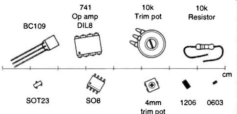
Fig.2 SMDs are much smaller than TH types - illustrations are approximately
actual size
3. Industrial SMT Circuit Production
It will be useful to review how commercial circuits are put together with modern SMT production machinery as some of the techniques can be adapted for small scale use. As expected we start with the PCB. This will have been designed on a CAD system and may range in complexity from something simple like a TV remote controller or the innards of a talking doll to a computer motherboard. The more complex PCBs may well have a multilayer construction consisting of up to eight layers of tracking. Multi-layering is another means of solving the inter connection problem with highly integrated circuits. Basic CAD systems for home PCs are already widely available and are in use by many hobbyists so no difficulty here. Most CAD systems contain Surface Mount pads or the facility to design them. After etching, cleaning and tinning, the PCB is coated with a solder mask. This (the green color seen on commercial PCBs) must be photographically processed to expose only the areas where chips are to be soldered. It is a very useful addition as it reduces the chance of solder bridging between fine IC pins for example. The availability of masking film is a problem for the amateur. But thankfully it is mostly unnecessary for hand working.
A small dab of solder paste is now applied to the component lands using a precision dispenser or by screen printing. Often a spot of glue will be applied to a dummy land where the center of the chip will rest. By the way this can make the salvaging of chip components from commercial PCBs a bit less productive as the glue is quite strong. The solder paste can have sufficient tackiness (green strength) to hold the chip in place obviating the need for an adhesive. Next the SMDs themselves are placed on the pads by a "pick and place" machine. There are many faster methods of placing SMDs on board such as chip shooters and simultaneous methods. This process is one of the marvels of SMT where chips are "picked" from supply tapes and "placed" in the exact position under computer control at impressive speeds as fast as 300,000 chips per hour. Such machines represent the "T" in SMT. For small scale production, manual "pick and place" and simple automatic machines are available. This approach might not appeal to the amateur but for schools, colleges and clubs it is not out of the question.
The populated PCB now continues on down the line and into a "reflow" oven. In a carefully controlled temperature profile the board is slowly raised to the solder paste reflow temperature and then cooled back. All the chips are thus soldered in place at once, an impressive sight. The soldermask restricts the spread of molten solder to the exposed land areas. Any misalignment of the chips is corrected as they can float on the molten solder to take up a central position by surface tension forces. The soldering process can involve very complex technology like hot inert gas, lasers and infrared. The use of solder paste is certainly an option for the amateur. Solder paste or cream is readily available and the reflow temperature is easily reached using one of the many hot air blowers on the market.
Solder pastes contain a high proportion of flux and other organic chemicals and they produce huge quantities of fumes on heating to the reflow temperature, around 180 C. Most formulations leave a lot of residue on the PCB which must be washed away with a suitable cleansing fluid. The message here for the amateur is to make use of some of the proprietary chemicals which are now available for PCB treatment. Even after normal soldering, it is good practice to clean and protect your circuit. A surface mount PCB is a work of art and a thing of beauty to us enthusiasts. This may seem a trivial point but it is worthwhile keeping aesthetics in mind at all stages with the aim of producing a good-looking piece of work. Delicate treatment of SMDs and cleaning is considered worthwhile by the mass producers, for hard economic reasons. You will find that such an approach will likewise increase your success rate.
4. The Place of SMT
Choosing a printed circuit for turning a theoretical schematic diagram into a working device may seem obvious but there are many other solutions. It will therefore be useful to consider the part played by SMT in present day circuit manufacture. The first active device was the thermionic valve and circuits in those early days were made in a style referred to as "breadboard" construction. This was a form of surface mount construction but individual devices and wiring were held in place with nuts and bolts. Since that time the "chassis" with point to point wiring underneath and valves on top, came and went. But the concept of components on one side and wiring (PCB tracks) on the other persisted. The printed circuit board with discrete through-hole components peaked and declined as most of the active circuit elements became integrated on silicon wafers.
The technique of wire wrap has found its niche but this is a means of interconnection rather than circuit fabrication. With surface mount fabrication we return to the concept of having components and wiring on the same side of the substrate.
Surface mount chips have had a long history in microwave construction and the concept has been ready to go for some time. Presently we have a right old mix of techniques. Among these we find Chip On Board (COB) construction in calculators and birthday cards which play a tune for you. This is an SM technique where the semiconductor die is mounted directly on the PCB by a variety of methods such as Tape Automated Bonding (TAB). This is not for the amateur constructor. As SMT developed it was common to find hybrid PCBs containing a mixture of SMDs and TH devices. About half of all main stream circuits now produced are fully surface mount and the proportion is steadily increasing. Only the capital already invested in TH insertion machinery has slowed down the introduction of SMT. SMT therefore has a very important place in circuit construction and is set to grow.
5. Amateur Construction with SMDs
Surface mount construction has many attractions for the hobbyist and its increasing use indicates that the advantages can be realised in practice. It is apparent that those constructors who try SM, soon develop the required skills and in fact strive to make it their main method of project construction. Their comments mostly refer to the simplicity of designing a PCB layout and the ease of soldering-in chip components without having to repeatedly turn the board over. From their point of view the complexity of using through-hole components seems quite pointless. Soldered-in SMDs are very secure. A certain pride is experienced in using state-of-the-art techniques and of course it is excellent self-training which could be employed in industry.
To gain wide usage by the amateur, SM must be able to compete with many very simple methods of getting a circuit up and running. In fact it has to compete with the unquestioned versatility of through-hole components. These include Veroboard and "ugly construction". The latter is a type of point to point construction using an unetched piece of PCB as a ground plane. The leads of the TH components are soldered end to end as required and are mostly self supporting in mid air.
This is a valid approach for simple experimental circuits with a couple of active devices. Similar methods can be developed with SMDs. They can be stood on end, on their sides, mounted piggyback and soldered end to end. You can even add a couple of wires making in effect a leaded component for bridging between parts of the circuit. Do's and don'ts will become apparent to the experimenter, for example the ends of chip resistors and capacitors are easily broken off. More important some of the layers in multilayer capacitors can become disconnected causing mysterious changes in circuit performance. Therefore with this lazy approach to our chosen art a little care is needed.
There is no direct equivalent to Veroboard at this time. Although some commercial suppliers offer small test PCBs they are primarily intended for soldering practice with dummy components. But why not make a small "protoboard" PCB for yourself, possibly using some of the techniques discussed later for PCB design and construction. A good example of this is shown in Figure 3. Inter-wiring links are easily made with fine wire or zero ohm jumpers. The 30 awg insulated Kynar wire used for wirewrap is ideal for longer runs and zero ohm jumpers for short bridges.
At the top end of the construction stakes we are looking at a custom-made PCB for your project. Surface mount has no problem competing here. The initial design is easier and coupled with the time saved in drilling, making a little PCB for your project is a far less daunting task than a through-hole PCB.
Once you are set up to produce PCBs, it is surprising how quickly a prototype circuit can be completed. After optimization by bridging, piggybacking and any other tricks you can think of, a final show model can be run off without drilling a hole or having to face the task of mirror image tracks, endless tossing and turning during soldering and clipping of pigtails.
It would therefore appear that SM components can compete with their cousins, certainly for all low-power functions and up to moderate output powers. We would normally consider SM to be aimed at the signal/low power level. At the power end of SMT, 3 watt (SOT223) transistors have been available for some time. Above a couple of watts we are into nuts and bolts but even so 20 watt SM power devices are receiving wide acceptance. A surface mount version of the LM386 audio power amp running at 0.5 watts will provide adequate output for many small radio projects. This is the subject of an SM project described later.
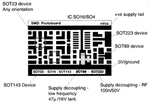
Fig.3 An SMD Protoboard (actual size)