AMAZON multi-meters discounts AMAZON oscilloscope discounts
In this section a number of preamplifier circuits will be described including
tone control circuits, and then should be a suitable design here for virtually
any normal audio preamplifier application.
Microphone Preamp.
Where high quality is required the most common types of microphone in use these days are probably electret types having a built-in preamplifier and step-up transformer, or dynamic types having a built-in step-up transformer. In either case the output level of the microphone is not normally very high, with a signal amplitude of only around 2 millivolts RMS being typical. This is far too small to permit such microphones to be used successfully with many items of audio equipment where the most sensitive input might require an input level of a few hundred millivolts RMS. Incidentally, although some items of equipment have an input for a magnetic pick-up with an input sensitivity of around 2 to 5 millivolts RMS, as we shall see later, an input of this type has a tailored frequency response and will not give satisfactory results if fed from a microphone.
This microphone preamplifier has a voltage gain of over 52dB (400 times) and will match a high impedance dynamic or electret microphone to virtually any piece of audio equipment. When used in conjunction with most microphones of these types an output level of about 1 volt RMS can be readily achieved, but a gain control enables a lower output level to be set so that overloading of the equipment fed with the output signal can be avoided. The signal to noise ratio of the unit is excellent, and is typically well over 70dB with reference to an output level of 1 volts RMS (at full gain, unweighted). As will be explained later, the circuit can be modified for use with a low impedance dynamic microphone or an electret type which does not have an integral step-up transformer.
The full circuit diagram of the Microphone Preamplifier is shown in Figure 1.
The circuit is a two stage type which uses ICI as a non inverting amplifier, and IC2 as an inverting amplifier (both are operational amplifiers of course). Both amplifiers are standard configurations. The closed loop gain of IC1 is set at about 45 times by negative feedback circuit R3 and R5. The input impedance of the circuit is set at a nominal figure of 27k by R4, and this is high enough to ensure that excessive loading of the microphone does not occur. C2 provides DC blocking at the input of the circuit. A set of break contacts on input jack JK1 are used to short circuit the input when no micro phone is connected to the unit. This eliminates any stray pick-up of electrical noise at the input, and also prevents possible oscillation due to stray feedback. The device used in the ICI position is a NE5534 or NE5534A high performance operational amplifier. The NE5534A is slightly better than the NE5534 for audio applications such as this one (although it is a little more expensive), but both devices give excellent performance with very low levels of noise and distortion. The circuit will work using other low noise, internally compensated operational amplifiers such as the 741C or TL071CP, but the noise performance of the NE5534 or NE5534A is noticeably superior to most of the alternative devices, and the additional cost of an NE5534 or NE5534A is usually well justified in a critical application such as this.
C3 couples the output of IC1 to VR1 which is a simple volume control type gain control. From here C4 couples the signal to the second stage of amplification. R6 and R9 form a negative feedback circuit which set the closed loop voltage gain of IC2 at ten times, giving the circuit a maximum total voltage gain of about 450 times. As far as noise performance is concerned, the ultimate in performance is not required from the device employed in the IC2 position since the signal level at the input to this stage is far higher than that at the input of IC1. Using a really low noise device here would not give any noticeable improvement in noise performance, and the TL081CP (or a similar device such as the LF351) give a more than adequate level of performance.
BIFET operational amplifiers such as the TL081CP and LF351 have very low levels of distortion, and the distortion produced ...
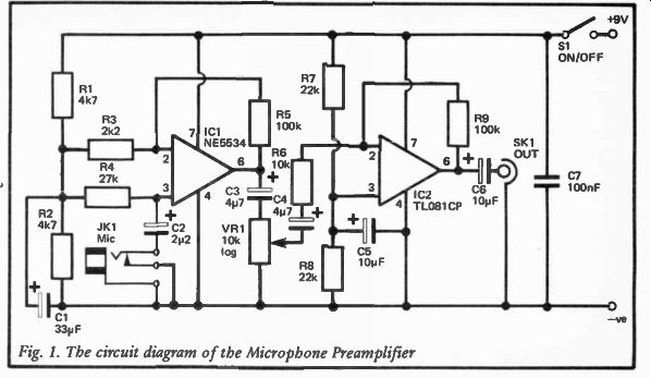
Fig. 1
... by the circuit is negligible provided the output level does not exceed about 2 volts RMS or so.
The current consumption of the circuit is about 6 milliamps, and this can be supplied economically by even a small 9 volt battery such as a PP3 or PP6 type. A higher supply potential of up to 30 volts can be used and a higher supply voltage gives the circuit a larger overload margin, but the current consumption increases somewhat at higher supply voltages.
Construction
A printed circuit board measuring 3.2 inches by 1.7 inches takes all the components except VR1 and the sockets. Figure 2 gives details of the component layout and wiring while Figure 3 shows the copper track pattern. The board is constructed in the normal way and is perfectly straight forward.
It may be possible to build the unit into some other item of equipment, or you may wish to construct it as a self contained preamplifier. If the latter is the case it is advisable to house the unit in a metal case which gives good screening from sources of electrical interference such as mains hum. A diecast aluminum box is ideal, and these also have the advantage of being extremely tough. SKI can be any convenient type of two way audio connector (jack, phono, etc.), but as JK I must be fitted with a break contact this really restricts the choice here to a standard 6.35mm or a 3.5mm jack, and the microphone plug must be changed accordingly if necessary.
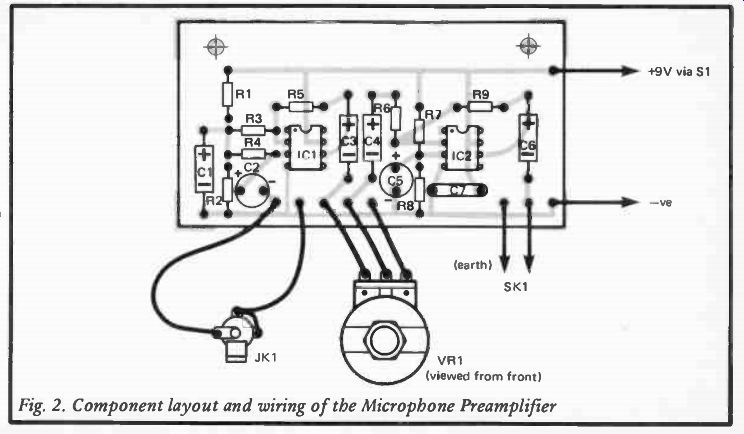
Fig. 2
Low Impedance Version
As mentioned earlier, the circuit can be modified to suit a low impedance microphone such as a dynamic type which does not have an internal step-up transformer, and this simply entails a few changes in component values. The input impedance of the circuit does not need to be as high for a low impedance micro phone, and R4 can therefore be reduced in value to 2k2. In order to maintain a good low frequency response C2 should be increased to 10µF in value. The gain of the circuit needs to be increased since the circuit must compensate for the loss of voltage gain provided by the step-up transformer in a high
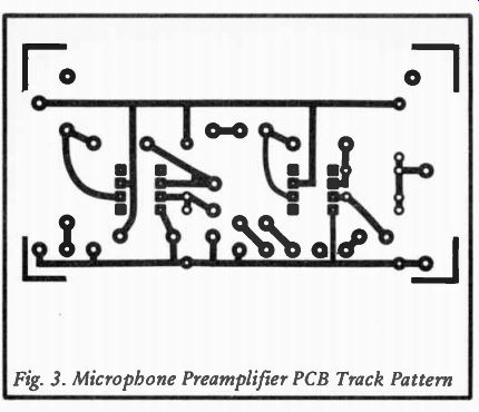
Fig. 3. Microphone Preamplifier PCB Track Pattern
impedance microphone. This can be accomplished by raising the value of R9, say to about 470k. An inevitable consequence of this boost in gain is a significant reduction in signal to noise ratio, although the circuit should be quite acceptable in this respect. However, wherever possible it is better to use a high impedance microphone and the circuit values shown in Figure 1.
Components for Microphone Preamplifier (Figure I)
Resistors, all miniature 1/4 watt 5%
R1 4k7 R2 4k7 R3 2k2 R4 27k R5 100k R6 10k R7 22k R8 22k R9 100k
VR1 10k log. carbon potentiometer
Capacitors
C1 33µF 16V axial electrolytic
C2 2u2 50V radial electrolytic
C3 4u7 50V axial electrolytic
C4 4u7 50V axial electrolytic
C5 10µF 16V radial electrolytic
C6 10, uF 16V axial electrolytic
C7 100nF polyester
Semiconductors
IC1 NE5534 or NE5534A
IC2 TL081CP or LF351
Sockets
JK1 3.5mm jack with single break contact
SK1 2 way audio connector
Miscellaneous
S1 SPST miniature toggle switch
Case
Printed circuit board
Control knob
9 volt battery (e.g. PP3)
Wire, battery connector, etc.
Tape Preamplifier
When used in conjunction with a suitable power supply and a cassette mechanism this simple playback amplifier makes a useful cassette player for use with a hi-fi system. Suitable cassette mechanisms are available quite cheaply on the surplus market from time to time, or it may be possible to obtain a suitable mechanism from a defunct cassette recorder. Alternatively a new cassette mechanism could be used, and these are available from one or two companies.
Equalization
Due to the low output signal level of a tape head and the comparatively high drive voltage required by most hi-fi amplifiers, a tape playback amplifier must give both high gain and a low noise level. Furthermore, the output from a tape head requires equalization since it provides an output that increases at a rate of 6dB per octave (i.e. a doubling of frequency causes the output voltage to be doubled). This is because a doubling in frequency causes a doubling in the rate at which the magnetic field changes, and the output voltage is dependent on both the field intensity and rate of change. This is actually the same effect that is obtained with a magnetic cartridge in a record player.
However, whereas a magnetic pick-up and a record work efficiently over the entire audio band, this is not true of normal magnetic tape systems. These become very inefficient at higher audio frequencies so that the rise in output first slows up, and then actually turns over to give a reduction in output. To a certain extent this reduction in efficiency is overcome by applying treble boost to the recorded signal, but this is not sufficient to maintain a 6dB per octave rise over the whole audio band.
In cassette systems the output from the tape head rises normally up to a frequency of approximately 2kHz, and then hardly increases at all at higher frequencies. The tape playback amplifier must therefore have a frequency response which is the inverse of this, and the required response is shown in Figure 4.
The slight roll-off at the low end of the response only really effects sub-audio signals, and is used merely to prevent any signals of this type from giving rise to undesirable effects. It also makes it easier to avoid low frequency instability.
The Circuit
Figure 5 shows the circuit diagram of the Tape Preamplifier, and this is for one channel only. The other channel is, of course, essentially the same.
An LM382 dual audio preamplifier integrated circuit is used at the input of the unit, one section of the device being used in each stereo channel. The pin numbers shown in Figure 5 are for the left hand channel; those for the right hand channel being shown in brackets. The supply connections are common to both channels. The LM382 is well suited to this application as it provides a low noise level, low distortion, and high gain.
It is also quite inexpensive, and is a convenient point at which to add the equalization.
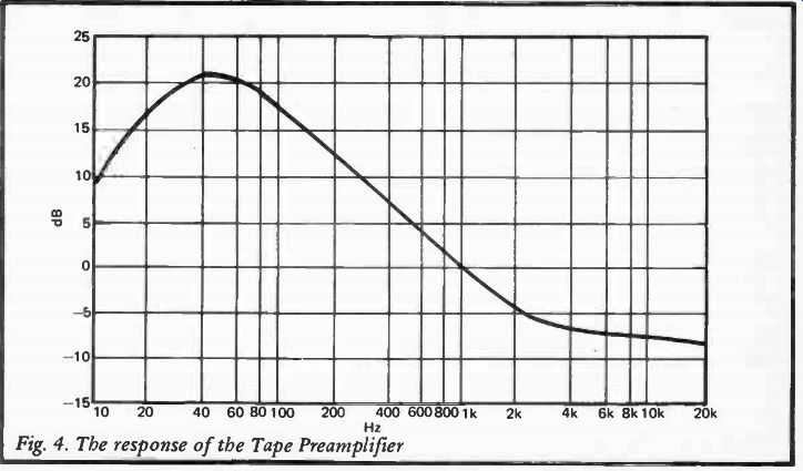
Fig. 4. The response of the Tape Preamplifier
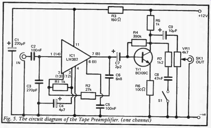
Fig. 5. The circuit diagram
of the Tape Preamplifier. (one channel)
The equalization is provided by R2 and C6 which are connected between the output and the inverting input of the preamplifier. At low frequencies C6 has a high impedance which consequently gives a low level of feedback and high voltage gain. At higher frequencies the impedance of C6 becomes progressively lower, giving increased negative feedback and rolling off the response of the circuit at the required 6dB per octave. This only continues up to a frequency of about 2kHz, as above this frequency the impedance of C6 becomes very low in comparison to that of R2, and does not have much effect on the level of feedback or voltage gain of the circuit.
R1 and C4 are also part of the feedback circuit.
C2 is the input DC blocking capacitor and C3 is an RF filter capacitor which helps to avoid problems with RF interference and instability due to stray feedback from the output to the non-inverting input (to which the input signal is coupled). The LM382 has a high level of supply ripple rejection, but due to the very low input signal level and the likelihood of noise spikes being coupled into the supply lines from the motor in the cassette mechanism, C1 and R3 are used to filter the supply to IC1.
Although IC1 provides a substantial amount of voltage gain it still gives an output level of only about 50mV RMS, which is about one tenth of the drive voltage required by most hi-fi amplifiers. Tr1 is therefore used as a common emitter amplifier having a voltage gain of about 20dB. R4 provides negative feedback which reduces the voltage gain of Tr1 to the correct level and also gives a lower distortion level. C9 couples the out put of Tr1 to variable output attenuator VR1.
It is likely that many of the cassettes played through the unit will be Dolby B encoded types, but unfortunately there are difficulties in incorporating a Dolby B decoder in a home constructed cassette player (licensing, adjustment, added cost and complexity). However, a certain amount of noise reduction can be obtained when playing Dolbyized cassettes simply by using a treble cut filter, and a reasonably flat overall frequency response can be obtained.
The Dolby B process operates by applying treble boost during recording, but the amount of boost applied depends on the dynamic level of the recorded signal. It is at a maximum during periods of low signal level, and reduces to zero at the highest dynamic levels. On playback the decoder applies treble cut to the signal, and the degree of treble cut again varies with dynamic level. In fact the treble cut exactly compensates for the treble boost used when recording so that a flat frequency response is produced. However, the treble cut used during playback reduces tape "hiss" during quiet passages when it is most intrusive. There is no noise reduction when the signal is at the highest dynamic levels, but this is unimportant since the noise is then totally masked by the signal anyway.
In this circuit S1 is closed when a Dolby B encoded cassette is played, and this switches into circuit a simple top cut filter which is comprised of R7 and C8. This filter gives an attenuation of about 5dB at frequencies of about 10kHz or more. The attenuation steadily decreases at lower frequencies, and is insignificant at middle and low frequencies. This results in high frequencies being boosted by about 5dB during periods of low signal level, and attenuated by about 5dB during periods of maximum dynamic level. At medium signal levels there is a roughly flat frequency response. Thus this simple arrangement gives a small but worthwhile reduction in noise plus a reasonably flat overall frequency response.
The performance of the playback amplifier is very good, but it must be borne in mind that the level of performance obtained from the player is determined by other factors such as the performance of the cassette mechanism, the playback head used, the recording tape, etc. The prototype gave very acceptable results when tried with good quality recordings and a surplus front-loading cassette mechanism.
Power Supply
The mains power supply circuit shown in Figure 6 is ideal for use with the Tape Preamplifier, and provided a 12 volt cassette mechanism is used it will power this as well. It can provide a maximum current of about 400 milliamps which is sufficient to operate any normal cassette mechanism even during fast forward or fast-rewind (when the current consumption is at its highest). The circuit is quite straight forward and uses full wave (bridge) rectification and a 12 volt monolithic voltage regulator to give a well smoothed and stabilized output. T1 is one of the common twin secondary types, and in this circuit the two secondaries are connected in parallel to effectively give a 15 volt 400 milliamp winding.
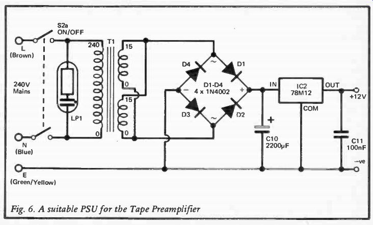
Fig. 6
Construction
Both channels of the playback amplifier can be accommodated on a 0.1in. matrix stripboard panel which has 41 holes by 18 copper strips. Figure 7 shows the component layout of this panel while Figure 8 shows the points at which the copper strips must be cut. Many of the component identifications are repeated in Figure 7, and this is where two of each component are required, one for each stereo channel. The only connections not shown in Figure 7 are the wires from the sliders of VR1 to the output sockets'(which were phono types on the prototype, but can be any preferred type). Of course, the two input leads must be screened, and in the interest of good channel separation it is advisable to use either separate leads or twin individually screened lead.
A suitable 0.1in. pitch stripboard layout for the power supply is shown in Figure 9, and this is based on a board which has 11 copper strips by 15 holes. There are no breaks in any of the copper strips.
Due to the high sensitivity of the playback amplifier, especially at low frequencies, the amplifier panel is quite sensitive to stray pick up of mains hum and other electrical noise. It is therefore advisable to mount the board where it is a reasonable distance away from T1 and the motor in the cassette mechanism.
IC2 requires a small amount of heatsinking and it may be possible to use the case as a heatsink if a metal type is used.
Alternatively a small finned (bolt on) heatsink should be adequate, and a heatsink of this type was used on the prototype.
In use VR1 will probably need to be adjusted for maximum output in order to give good results. However, a few amplifiers have high sensitivity and with such units it will be necessary to back-off VR1 somewhat, otherwise the volume control of the amplifier will operate rather abruptly.
It is just possible that the output of the unit will not be high enough to drive some amplifiers properly. If this should be the case a simple solution to the problem is to reduce the two R6s to 47 ohms in value. This boosts the gain of the output amplifiers and gives increased output.
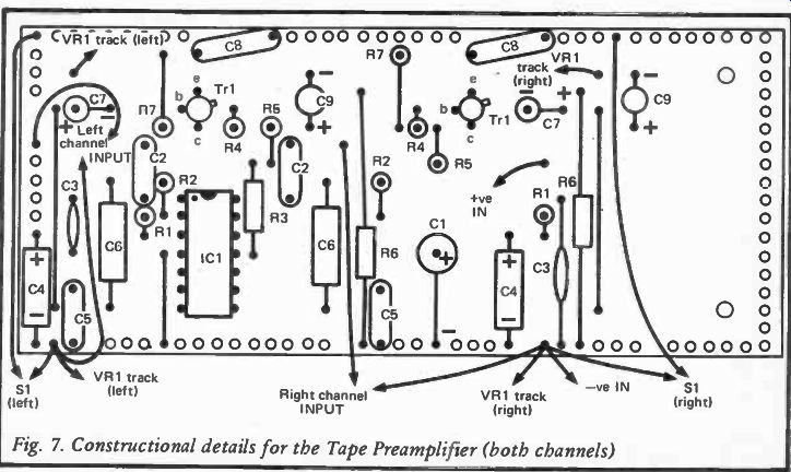
Fig. 7. Constructional details for the Tape Preamplifier (both channels)
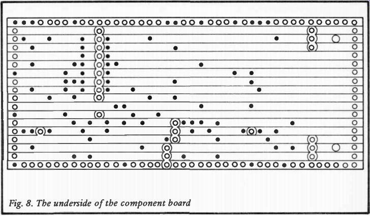
Fig. 8. The underside of the component board
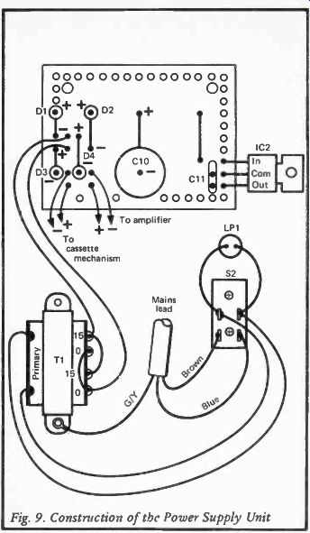
Fig. 9. Construction of the Power Supply Unit
Components for Tape Preamp and Power Supply (Figure 5 & 6)
Resistors, all % watt 5%
*R1 R3
*R5
*R7 VR1 1k *R2 27k 150 ohms *R4 390k 1k *R6 100 ohms 1k2 4k7 log, dual gang carbon
Capacitors
C1 220µF 25V
*C3
*C5 sc.9 C1 1 270pF ceramic plate 100nF type
C280 2122 25V 10µF 25V 100nF type C280
*C2 100nF type C280
*C4 4127 25V
*C6 6n8 polystyrene 5%
*C8 47nF type C280
C10 2200µF 25V
Semiconductors
IC1 LM382 IC2 78M12 (12 volt 500mA Tr1 BC109C positive regulator)
D1 to D4 1N4002 (4 off)
Switches
S1 DPST rotary switch
S2 DPST toggle switch
Transformer
T1 Standard mains primary, twin 15 volt 200mA secondaries
Miscellaneous Case
Two control knobs
0.1in. matrix stripboard panels
Panel indicator neon having integral series resistor for normal mains usage (LP1)
Cassette mechanism (see text)
Two phono output sockets Mains lead, connecting wire, screened lead, solder, etc.
(Note that where a component is marked "*", two of this item are required, one for each stereo channel).
Guitar Preamplifier
The output signal level from guitar pick-ups seems to vary quite considerably from one pick-up to another, and while some provide a very high output which can drive practically any power amplifier, others provide an output of only about 30 millivolts RMS or so. Amplifiers specifically designed for use with guitars normally have a fairly high sensitivity so that they can be used successfully with practically any pick-up, but when using a guitar with some other type of amplifier (such as a hi-fi amplifier) it is often found that the maximum volume obtained is inadequate.
A simple solution to the problem is to use a preamplifier to boost the signal level prior to feeding it to the power amplifier.
The simple design described here has a voltage gain which can be varied from unity to over 26dB (20 times), and it should therefore match virtually any guitar pick-up to virtually any power amplifier. The input impedance of the preamplifier is about 50k and the output impedance is low. Thus the circuit can be used with unity voltage gain as a simple buffer amplifier, if it is necessary, to match the relatively high output impedance of a guitar pick-up to a power amplifier having a low input impedance.
The Circuit
A single low noise B1FET operational amplifier (IC1) is used as the basis of the unit which consequently has negligible distortion levels and a signal to noise ratio that will be about -70dB or more even if the unit is used with a very low output guitar. Figure 10 shows the full circuit diagram of the Guitar Preamplifier.
This is just a straight forward operational amplifier non inverting mode circuit with R2 and R3 being used to bias the non-inverting input of IC1 to about half the supply voltage.
These also set the input impedance of the circuit at about 50k.
R1 and R4 are the negative feedback network, and with R4 at ...
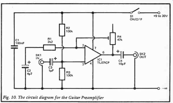
Fig. 10. The circuit diagram for the Guitar Preamplifier
... minimum value the inverting input and output of IC1 are directly connected to one another and the circuit has unity voltage gain. As R4 is adjusted for increased resistance value the AC voltage gain steadily increases, but C2 provides DC blocking so that the DC voltage gain remains unity, and the output of the amplifier remains biased at half the supply voltage. The voltage gain of the amplifier is approximately equal to R1 plus R4, divided by R1, and this gives a nominal maximum voltage gain of just over 22 times with R4 at maximum value.
The current consumption of the circuit is about 2 milliamps with a 9 volt supply, rising to around 2.5 milliamps with a 30 volt supply. A small 9 volt battery such as a PP3 type is a suitable power source for the unit. The maximum unclipped output level is about 2 volts RMS using a 9 volt supply, and this should be perfectly adequate. Note that a well smoothed and ripple free supply is required, and it may be necessary to use a simple R-C filter in the positive supply lead in order to obtain a low level of mains hum on the output if a simple mains power supply is used.
Construction
A 0.1in. matrix stripboard having 22 holes by 13 strips is used as the constructional basis of the amplifier, and Figure 11 provides full details of this board. Construction of the component panel is carried out using the usual techniques and is perfectly straightforward. As for any sensitive preamplifier, it is advisable to use a metal case such as a diecast aluminum type. SK1 and SK2 were both 6.35mm jacks on the prototype, and although these will probably be the most convenient type for this application, they can obviously be changed for an alternative type if this would be more convenient in use.
For optimum results R4 should be set for the lowest level of gain that gives satisfactory results. This gives the lowest possible noise and distortion levels, and minimizes any slight risk of problems with the amplifier being overloaded. Note that the gain of the circuit is unity with R4 set fully clockwise, and at maximum with this component set fully anticlockwise.
If the unit is to be used with different guitars and (or) amplifiers ...
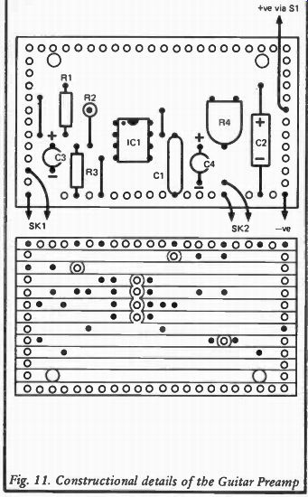
Fig. 11. Constructional details of the Guitar Preamp
...it might be better to replace R4 with a potentiometer mounted on the front panel of the unit so that the gain of the amplifier can be adjusted more easily.
Components for Guitar Preamplifier (Figure 10)
Resistors, 1/4 watt 5% except R4 R1 2k2
R2 100k
R3 100k
R4 47k 0.1 watt horizon preset
Capacitors
C1 100n F polyester
C2 4u7 50V axial electrolytic
C3 le 50V rad. Electrolytic
C4 10e 25V rad. electrolytic
Semiconductor
IC1 TL071CP
Miscellaneous
S1 SPST toggle switch
SK1 6.35mm jack
SK2 6.35mm jack
0.1in. matrix stripboard
Case
Battery, battery connector, wire, etc.
High Impedance Buffer Amplifier
Sometimes an amplifier having an extremely high input impedance is required, such as when using a crystal or ceramic pick-up, or at the input of a piece of audio test equipment. In the case of the latter the high input impedance is needed since minimal loading of the circuit under test is essential in order to produce reliable results. With ceramic and crystal pick-ups the problem is that the pick-up is effectively a voltage generator in series with a capacitor of typically 2 to 20 nanofarads in value. If a pick-up of this type is fed into a low impedance load a simple highpass filter is formed by the capacitance of the pick-up and the input impedance of the amplifier, and this filter severely attenuates the bass and possibly even the middle frequency response of the system. With a very high load impedance the highpass filter action is still produced, but as the cut-off frequency is below the lower limit of the audio spectrum this is of no practical significance.
The buffer amplifier featured here has a very high input impedance of typically over 100 megohms at 1-kHz, and the input impedance can be easily changed to any desired figure below this level. The voltage gain of the circuit is unity.
The Circuit
Figure 12 shows the circuit diagram of the High Impedance Buffer Amplifier, and the unit is basically just an operational amplifier used as a unity gain non-inverting amplifier. By coupling the output of IC1 direct to its inverting input 100% negative feedback is applied over the device so that the required unity voltage gain and very high input impedance are obtained.
However, the bias circuit, which in this case consists of R1 to R3, shunts the input impedance of the amplifier so that the circuit as a whole has a far lower input impedance than IC1 alone. The input impedance is still around 2.7 megohms, and this is adequate for most applications.
The shunting effect of the bias resistors can be eliminated though, and this is the purpose of "bootstrapping" capacitor C2. This couples the output signal to the junction of the three bias resistors, and any change in input voltage is therefore matched by an identical change in voltage at the output of IC1 and at the junction of the three bias resistors. This gives a constant voltage across R3, and any change in the voltage at one end of R3 produced by the input signal is counteracted by an identical change in potential at the other end of R3. This resistor has an apparent infinite resistance as far as the input signal is concerned since this signal does not generate any potential difference across R3 or produce any current flow through this component, and the shunting effect of the bias resistors is totally eliminated.
A standard 741C operational amplifier is used in the IC1 position, and as mentioned earlier this gives an input impedance which is typically in excess of 100 megohms at 1kHz, which should be more than adequate for any normal application. The higher input impedance that could be obtained using a FET input operational amplifier is not really of any practical value, and there are a couple of disadvantages to using most FET input devices in this circuit. One is simply that they have a tendency...
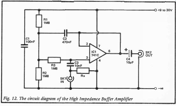
Fig. 12. The circuit diagram of the High Impedance Buffer Amplifier
...to oscillate when the input is open circuit (the oscillations are damped down and removed when an input is connected to the unit). The second is that most FET input devices have a significantly higher input capacitance than bipolar devices such as the 741C. Thus the shunting effect of this capacitance would actually give a lower input impedance at most frequencies, and would only give a higher input impedance at lower-middle and bass frequencies.
If a comparatively low input impedance is required for some reason (such as for use with pick-up which has a recommended load impedance of several hundred kilohms or a few megohms)
one way of achieving this is to remove C2 and adjust the values of RI to R3 to give the desired input impedance. A simple alternative is to simply add resistor Rx, and the input impedance will be approximately equal to the value of the component used here.
Construction
The buffer amplifier is built on a small printed circuit board, as detailed in Figures 13 and 14, and construction should present no difficulties. There is provision on the board for resistor Rx incidentally. The circuit will operate satisfactorily from any supply potential from 9 to 30 volts with a current consumption of about 2 milliamps. The maximum peak to peal output voltage is about 4 volts less than the supply voltage.
Components for High Impedance Buffer Stage (Figure 12)
Resistors, all 1/4 W 10%
R1 1M8
R2 1M8
R3 1M8
Rx See text
Capacitors
C1 100nF polyester
C2 470nF carbonate
C3 10nF polyester
C4 10µF 25V axial electrolytic
Semiconductor
IC1 741C
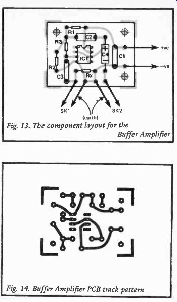
Fig. 13. The component layout for the Buffer Amplifier; Fig. 14. Buffer Amplifier
PCB track pattern
Miscellaneous
Case
Printed circuit board
Input and output sockets (SK1 and SK2)
Wire, etc.
Tone Controls
A tone control or tone controls seems to be a feature of almost every audio amplifier regardless of its intended application, and even quite simple pieces of audio equipment such as portable cassette players and radios seem to have a simple tone control these days. Tone controls range from a simple top-cut control which can be used to attenuate high frequencies and reduce background "hiss" to graphic equalizers. Probably the most common and popular type of tone control system is the type where there are separate bass and treble controls which are each capable of providing several dB of boost or cut. These give a great deal of control over the reproduced sound, but need only quite simple and inexpensive circuitry.
The tone controls described here are of this normal bass and treble type, and the next section of this guide covers a simple central tone control which can be used in conjunction with this design (or any other bass and treble tone control system) to give a slightly more sophisticated three tone control circuit.
The circuit is an active type which gives nominally unity voltage gain, and this type of circuit is very easy to fit into an audio system since it does not introduce problems of inadequate or excessive gain if it is added between (say) a preamplifier and a power amplifier which operate satisfactorily when directly coupled together. This is not the case with passive circuits which give losses of about 20dB, and some active circuits which give around 20dB of gain. The circuit provides a maximum boost of about 12dB at 100 Hertz and 10 kilohertz,' and similar level of maximum cut.
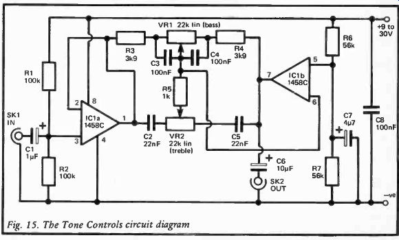
Figure 15
The Circuit
Figure 15 shows the full circuit diagram of the Tone Controls.
IC1a is a straight forward unity gain buffer stage which ensures that the tone control circuit is fed from a suitably low source impedance, and it also gives the circuit a reasonably high input impedance of about 50 kilohms.
The main tone control circuit is built around IC1b which is used as an inverting amplifier, and frequency selective negative feedback is used to provide the boost or cut in gain at high and low frequencies. VR2 is the treble control, and this works in conjunction with C2, C5 and R5. With the slider of VR2 towards C2 there is a relatively high impedance from the output of IC1b to its inverting input, and a low impedance from the output of IC1a to the inverting input of IC1b. These two impedances form a negative feedback network over IC1b and give the circuit a significant voltage gain of about 12dB. With the wiper of VR2 towards C5 there is a low impedance from the output of IC1b to its inverting input, and a comparative high impedance from the output of IC1a to the inverting input of IC1b. This gives a very large amount of negative feedback and the circuit consequently gives less than unity voltage gain with losses of around 12dB or so. However, this only occurs at high frequencies where C2 and C5 have an impedance which is very low in relation to the value of VR2. At middle and low frequencies these two capacitors have a very high impedance so that the two feedback impedances are virtually identical, and the setting of VR2 has very little effect. Thus the required boost and cut at treble frequencies is produced, with unity voltage gain at middle and bass frequencies. R5 is included to limit the maximum boost and cut at very high frequencies to a reasonable level.
The bass control circuit operates in a similar manner. VR1 controls the amount of feedback applied to IC1b, but only at low frequencies. At middle and high frequencies C3 and C4 have a very low impedance in relation to that of VR1 so that VR1 is effectively short circuited. R3 and R4 then act as the negative feedback network and give unity voltage gain as they are equal in value. A secondary function of R3 and R4 is to limit the maximum amount of cut and boost provided by the circuit at very low frequencies.
Any supply voltage from about 9 to 30 volts can be used to power the circuit, and the current consumption is about 2.5 milliamps.
Construction
Figure 16 shows a suitable 0.1in. matrix stripboard layout for the Tone Controls, and this is based on a board measuring 24 holes by 17 copper strips. Construction of the board is quite simple, but be careful not to omit the four breaks in the copper strips (between IC1's two rows of pins) or the three link wires.
Also make sure that the track connections to VR1 and VR2 are the right way round, so that clockwise adjustment produces boost, and counter clockwise adjustment gives cut.
The unit could be constructed as a self contained unit for use between two items of equipment, but in most cases it will probably be possible to build the controls as part of a larger project. In either case it will be necessary to make up two component boards for stereo operation, and dual gang potentiometers would then be used for the two VR1 s and the two VR2s.
Components for Tone Controls (Figure 15)
Resistors, all 1/4 watt 5%
R1 100k R2 R3 3k9 R4 R5 1k R6 R7 56k
VR1 22k lin, carbon potentiometer
VR2 22k lin, carbon potentiometer
Capacitors
C1 1uF 63V radial
C2 electrolytic
C4 C3 100n F polyester
C6 C5 22nF polyester
C7 4u7 63V radial
C8 electrolytic
Semiconductor
IC1 1458C
Miscellaneous
0.1in. matrix stripboard
Wire, sockets, control knobs, etc.
100k 3k9 56k 22nF polyester
100nF polyester
10µF 25V axial electrolytic
100nF polyester
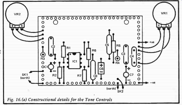
Fig. 16(a)
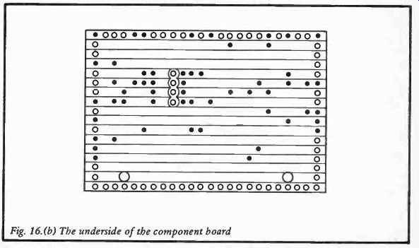
Fig. 16(b) The underside of the component board
Center Tone Control
This tone control exerts maximum control at a frequency of about 900 Hertz, and provides about 12dB or so of boost and cut. This circuit is really only intended for use with conventional bass and treble controls (such as the circuit described in the previous section of this guide), and is not of great value when used alone.
The Circuit
The circuit as shown in Figure 17, is a gyrator type, and is much the same as the filters commonly used in graphic equalizers.
Operation of the circuit is quite complex, but basically IC1 a is used as an amplifier, and IC1b is used to simulate an inductor which gives the desired shaping of the amplifier's frequency response.
The specified values for C4 and C5 give the filter a center frequency of approximately 900 hertz, as mentioned above, and this is about optimum for use with most bass and treble tone control circuits.
However, if necessary the center frequency can be altered by using a different value for C4 and CS, but bear in mind that changes in value produce an inversely proportional change in center frequency (e.g. a doubling of value halves the center frequency).
VR1 is the tone control potentiometer, and the circuit has approximately unity voltage gain and a flat frequency response with this control at a mid-way setting. The Q of the filter is not very high, and VR1 therefore has a significant effect on the gain of the circuit over quite a wide frequency range, but in this application this is not a disadvantage. In fact a high Q value with only a narrow range of frequencies being controlled would give unusable results in this application.
The current consumption of the circuit is about 2.5 milliamps.
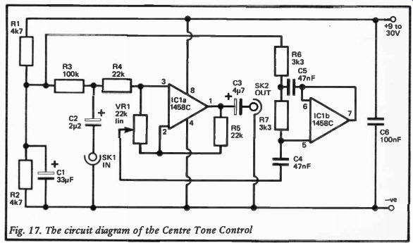
Fig. 17. The circuit diagram of the Center Tone Control
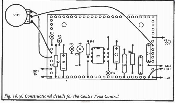
Fig. 18 (a)
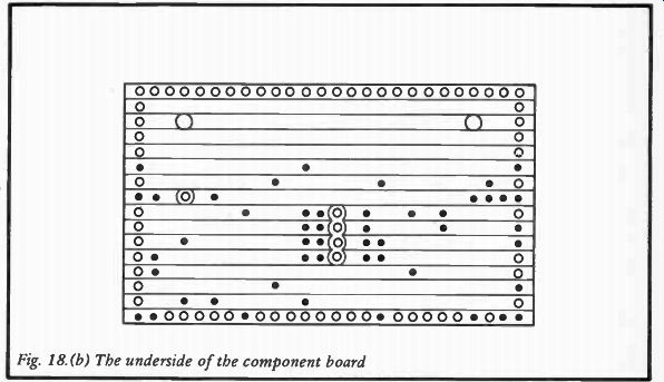
Fig. 18.(b) The underside of the component board
Construction
The Center Tone Control can be constructed on a piece of 0.1in. pitch stripboard using the component layout shown in Figure 18. This requires a board having 16 copper strips by 26 holes. Do not overlook the break in the copper strips which is required in addition to the four breaks between IC1's two rows of pins. Only three link wires are used. With VR1 wired a: shown in Figure 18 clockwise adjustment provides boost and anticlockwise adjustment gives cut.
Like the tone control circuit described earlier, this circuit has nominally unity voltage gain and it should not therefore produce any problems if it is added into a signal path. The only point to bear in mind is that the unit should not be connected where it will process a very low signal level (less than about 50 millivolts RMS) or it may significantly degrade the signal to noise ratio of the audio system. Similarly, it should not have an input level which (in terms of peak-to-peak voltage) is more than about 4 volts below the supply voltage used, otherwise clipping and severe distortion will result. If the circuit is used to provide boost, then the maximum acceptable input signal is reduced by an amount which is equal to the boost provided by the circuit. Obviously a fairly high supply potential of around 15 to 30 volts is advisable if the unit is to be used to handle a high level signal. These points also apply to the bass and treble tone controls described earlier, incidentally.
Components for Center Tone Control (Figure 17)
Resistors, all% watt 5%
R1 4k7 R2 4k7 R3 100k R4 22k R.5 22k R6 3k3 R7 3k3 VR1 22k lin, carbon potentiometer
Capacitors
C1 33µF 16V axial C2 2µ2 50V axial electrolytic
electrolytic C3 4127 50V axial or C4 47nF polyester radial electrolytic
C6 100nF polyester C5 47nF polyester
Semiconductor
IC1 1458C
Miscellaneous
0.1in. matrix stripboard
Control knob
Connecting wire
RIAA Preamplifier
The output from a magnetic or high output moving coil cartridge is normally in the 2.5 to 10 millivolt range, and a fairly sensitive preamplifier is therefore needed in order to match such a pick up to a power amplifier (which is likely to need an input signal of a few hundred millivolts RMS). Although the output of magnetic and moving coil cartridges rises at 6dB per octave it is not necessary to include equalization to counteract this since suitable equalization is used during the recording process.
However, equalization is still needed since bass cut and treble boost are applied during the recording process, in addition to the tailoring of the frequency response that is used to counter act the 6dB octave rise in output of the pick-up. The bass cut is used to prevent excessive groove modulations at low frequencies, and the treble boost (in conjunction with the treble cut during playback) provides a simple but effective form of noise reduction.
Figure 19 shows the required frequency response of an amplifier designed as a playback amplifier for normal RIAA standard recordings. Practical RIAA equalization amplifiers usually deviate slightly from this ideal response even if factors such as component tolerances are not taken into account, but even using a simple equalization network consisting of two resistor-capacitor pairs a maximum error of no more than about one or two dBs usually results, and this is perfectly satisfactory in practice.
The Circuit
An NE5534 or NE5534A operational amplifier is used as the basis of this RIAA preamplifier, as can be seen from the circuit diagram which is given in Figure 20. ICI is used in the non-inverting mode, and the non-inverting input is biased to about half the supply potential by R1 and ...
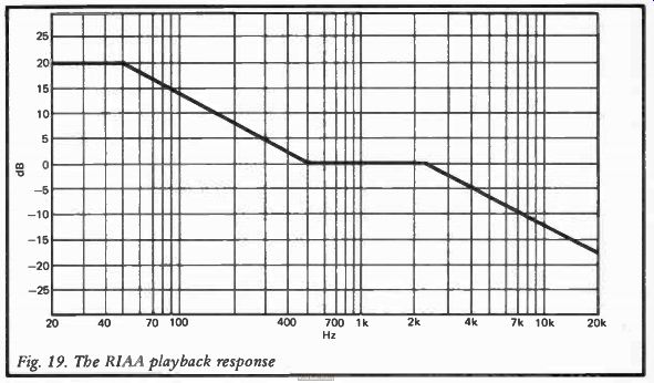
Fig. 19. The R1AA playback response
Fig. 20
... R2, with R3 being used to couple this bias voltage to IC1. C2 filters out any hum or other noise on the supply lines and prevents this noise from being coupled to the input of the amplifier. The high value of R3 gives the circuit a high input impedance, but this is shunted to the required level of about 47k by R4. Some pick-ups have an optimum load impedance of 100k, and if the unit is to be used with a pick-up of this type R4 should be increased to 100k. The high input impedance of the amplifier enables a fairly low value component to be used in the C3 position without compromising the bass response of the circuit, and this is beneficial as it avoids having a large surge of current through the pick-up at switch-on as this component takes up its normal operating charge. The required tailoring of the circuits frequency response is obtained using frequency selective negative feedback over IC1. At middle frequencies the gain of the circuit is largely determined by R5 and R7, but at lower frequencies C6 adds a significant impedance in series with R5 so that reduced negative feedback and the required increase in gain is produced.
Similarly, at high frequencies the impedance of C5 becomes low in comparison to that of R5, and the shunting effect of C5 produces increased feedback and the required high frequency roll-off.
As the circuit provides over 50dB of voltage gain at middle audio frequencies it will give a high enough output voltage to drive any normal power amplifier even if it is used with a cartridge which only gives an output of around 2.5mV RMS. The circuit will operate from any supply voltage of between about 9 and 30 volts, but the use of a fairly high supply potential (about 20 to 30 volts) is recommended in order to give a reasonable overload margin. If the circuit is used with a high output pick-up and a supply voltage of only about 9 volts it is quite likely that at least slight overloading will occur.
The signal to noise ratio obtained depends on the output level and source impedance of the particular pick-up used, but the low noise level of the NE5534 plus the relatively low voltage gain of the circuit at high frequencies give excellent results in this respect with a typical signal to noise ratio of well over 70dB. The NE5534 also gives low levels of distortion.
A supply current of only about 4 milliamps is required by the circuit.
Construction
The unit can be built as a self contained preamplifier, for use between a magnetic pick-up and a power amplifier which does not have a suitable built in preamplifier perhaps, or for use with a hi-fi amplifier which has a built-in RIAA preamplifier, but one which has a level of performance which leaves something to be desired. If constructed in this way the unit should be housed in a metal case and if a mains power supply is used it should be separated as far as possible from the preamplifier circuitry. The circuit has good ripple rejection and it is not essential to use a particularly well smoothed supply.
Of course, the unit can also be constructed as part of a larger project such as an integrated hi-fi amplifier or receiver. In either case the printed circuit layout shown in Figure 21 (component layout) and Figure 22 (track pattern) can be employed. This is for a mono unit, and for stereo operation it will be necessary to make up two boards, one for use in each stereo channel.
lf, in use, the gain of the circuit seems to be excessive (which it is quite possible if a high output cartridge or sensitive power amplifier is used) the gain of the circuit can be reduced somewhat by making R7 higher in value.
Components for RIAA Preamplifier (Figure 20)
Resistors, all watt 5%
R1 27k
R3 1M
R5 100k
R7 270 ohms
R2 27k
R4 47k
R6 1M2
Capacitors
C1 100nF polyester
C2 33pF 16V axial
C3 22nF polyester electrolytic
C5 1nF mylar
C4 10pF 25V axial
C7 15pF 25V axial electrolytic
electrolytic
C6 3n3 mylar
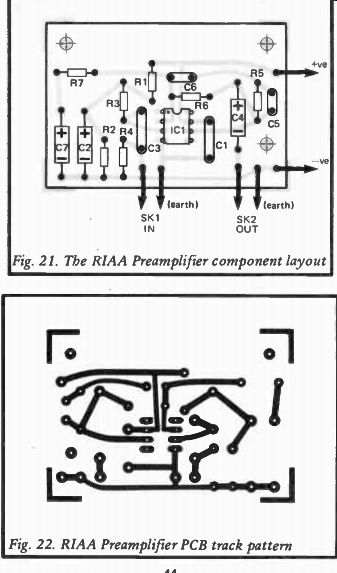
Fig. 21. The RIAA Preamplifier component layout; Fig. 22. RIAA Preamplifier PCB
track pattern
Semiconductor
IC1 NE5534A
Miscellaneous
Printed circuit board
Input and output sockets (SK1 and SK2)
Case Wire, etc.
Cont. to: POWER AMPLIFIERS
Also see:
Using Scopes in Transistor Circuits (1968)
Practical TRANSISTOR Servicing (1967)
Principles Of Transistor Circuits [1959]