AMAZON multi-meters discounts AMAZON oscilloscope discounts
Prev: PRE-AMPLIFIERS
In this section a number of power amplifier designs will be described ranging from simple low power integrated circuit based designs to high power MOSFET types. An 18 watt amplifier which operates from a 12 volt supply (for applications such as a car radio booster) is also included.
800mW Amplifier
For low power applications integrated circuit power amplifiers tend to give better results and reliability than discrete equivalents and are generally a little cheaper to construct as well. There are numerous audio power amplifier devices available, and these are all capable of a worthwhile level of performance. The integrated circuit used in this design is the ULN2283 (which is often just shown as the 2283 in retailers lists), and this device requires few discrete components to produce a complete amplifier circuit. It will work on a wide supply voltage range of 3 to 12 volts, and the output quality is more than adequate for a small power amplifier (where the loudspeaker used is normally the main limiting factor on output quality). Figure 23 shows the circuit diagram of the 800mW audio power amplifier. Apart from the supply connections (including four pins which connect to the negative supply) there are only three other terminals on the ULN2283. One is the output, and this is coupled to the loudspeaker by way of DC blocking capacitor C3. Like most integrated circuit power amplifiers the ULN2283 has a class AB output stage.
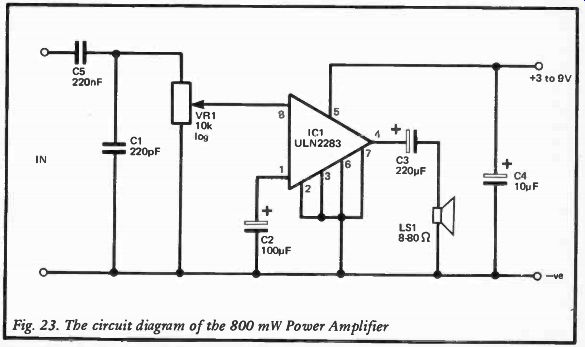
Fig. 23. The circuit diagram of the 800 mW Power Amplifier
Pin 1 of IC1 is the inverting input and an internal negative feedback circuit of the device connects to this input. This feedback network requires a discrete DC blocking capacitor, and in this circuit this component is C2. The feedback circuit gives the device a typical voltage gain of 43dB (about 140 times). The non-inverting input is pin 8, and this requires a bias resistance of about 100 kilo-ohms or less to the negative supply rail. In this circuit volume control VR1 provides the required biasing. C5 prevents DC inputs from being coupled to IC1 (and upsetting its biasing). C1 is used to filter out stray feedback at radio frequencies which could otherwise cause instability if the input of the amplifier was to be left open circuit, or if it is fed from a fairly high source impedance. C4 is a supply decoupling capacitor.
The output power of the circuit depends on the supply voltage and speaker impedance selected. Using a 9 volt supply and an 8 ohm loudspeaker an output power of about 800mW RMS can be achieved. Lower supply voltages and higher impedance loudspeakers give a correspondingly lower output power, with only about 170mW RMS being possible using a 4.5 volt supply and an 8 ohm impedance loudspeaker. The efficiency of the circuit inevitably reduces somewhat at lower supply voltages. In order to obtain a reasonable output power using a low supply voltage it is therefore necessary to use an 8 ohm loudspeaker and not a high impedance type. An output power of about 875mW can be achieved using a 12 volt supply and a 16 ohm impedance loudspeaker. Note though, that the use of a 12 volt supply and 8 ohm (or lower) impedance loudspeaker is not recommended, and that the supply potential must not exceed 12.5 volts.
The quiescent current consumption of the circuit is about 10 milliamps using a 6 volt supply, 12 milliamps with a 9 volt supply, or 17 milliamps using a 12 volt supply. However, the current consumption increases considerably at high output powers, and can rise to more than 100 milliamps. A large battery such as a PP9 type would therefore be needed if the unit is used with a 9 volt supply into an 8 ohm loudspeaker.
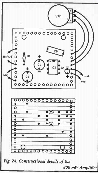
Fig. 24. Constructional details of the 800 mW
Amplifier Construction
A suitable stripboard layout for this amplifier is given in Figure 24, and this is based on a 0.1in. pitch board which measures 15 holes by 14 copper strips. There are no link wires, but do not overlook the two breaks in the copper strips.
For some applications the gain of the unit may be too high, with an input of only about 20mV RMS being needed to produce maximum output. The input sensitivity can be reduced by adding a resistor in series with the input to the amplifier, and as the circuit has an input impedance of about 10 kilohms a 10 kilohm resistor halves the sensitivity, a 20 kilohm component reduces sensitivity by a factor of three, a 30 kilohm resistor reduces it by a factor of four, and so on.
Components for 800mW Amplifier (Figure 23)
Resistor
VR1 10k log, carbon potentiometer
Capacitors
C1 220pF ceramic plate C2 100µF 10V radial C3 220µF 10V radial electrolytic
electrolytic C4 10µF 25V radial C5 220nF carbonate electrolytic Semiconductor
IC1 ULN2283
Miscellaneous
LS1 Loudspeaker having an impedance in the range 8 to 80 ohms
0.1in. matrix stripboard ( 15 holes by 14 strips)
Control knob
Wire, etc.
2 Watt Amplifier
This amplifier is based on the TBA820 integrated circuit, and although the TBA800 series of devices are far from new, they are very useful components which are probably as popular now as when they were first introduced. The TBA820 can provide an output power of up to 2 watts RMS using a 12 volt supply and an 8 ohm impedance loudspeaker. It can be used with higher impedance loudspeakers and supply voltages down to as little as 3 volts, but in either case the maximum output power is, of course, reduced. The TBA820 is excellent for use in battery powered equipment as it has a class B output stage which gives a quiescent current consumption of only about 4 milliamps (but bear in mind that the consumption can rise to as much as 250 milliamps or so when the amplifier is providing the full 2 watts RMS maximum output power).
The Circuit
As can be seen from the circuit diagram of Figure 25, the TBA820 requires a few more discrete components than many audio amplifier ICs, but in certain respects some of these additional components provide greater versatility and improved performance. Components which do not fall into this category are C4 and C6 which are merely needed to prevent high frequency instability.
Pin 5 is the inverting input of IC1, and there is an internal 6 kilohm resistor between this input and the output of the device.
This enables the voltage gain of the amplifier to be controlled by an external resistor and DC blocking capacitor, and the voltage gain is approximately equal to the value of the internal resistor divided by the value of the discrete resistor. This enables the gain of the amplifier to be adjusted over quite wide limits, and good stability is maintained within these limits. It is advisable not to make R1 less than about 22 ohms or the output quality may noticeably deteriorate, and a value of more than about 220 ohms might give poor stability. The specified value for RI gives a voltage gain of just over 40dB (one hundred times).
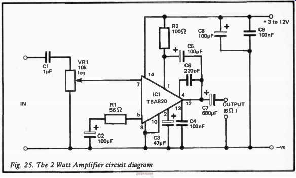
Fig. 25. The 2 Watt Amplifier circuit diagram
VR1 is the volume control and is also used to bias the non inverting input of IC1 to the negative supply rail. C1 provides DC blocking at the input of the amplifier. C3 decouples the supply to the preamplifier stages of IC1, and this helps to give the circuit good ripple rejection. This enables the circuit to be powered from a simple mains power supply without an excessive hum level being evident on the output, but for battery operation C3 will probably be of little or no help.
C5 and R2 are boot-strapping components, and this technique helps to give the circuit good efficiency. It is especially useful if the circuit is run from a low voltage supply, and then provides a significant boost in output power. R2 forms part of the collector load for the driver transistor of IC1, and by coupling the output signal back to R2 via C5 the supply voltage to the driver stage is taken above the positive supply potential on positive output half cycles. Normally the voltage drop through the output transistors of an amplifier limits the maximum output voltage to about one volt or more below the positive supply voltage, but the effective boost in the supply voltage to the driver stage provided by bootstrapping enables the output of the amplifier to achieve nearly the full supply potential.
Supply decoupling is provided by C8 and C9 while C7 is the output coupling capacitor.
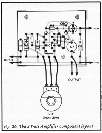
Figure 26
Construction
A suitable printed circuit design for this amplifier is provided in Figures 26 and 27. The component layout is quite compact and it is essential to use modern miniature capacitors if all the components are to be comfortably accommodated on the board.
The TBA820 has an unusual 14 pin quad-in-line (QI L) package which should plug into the printed circuit board without any difficulty. Make sure you obtain the TBA820 and not the TBA820M (which is basically the same device, but is in an 8 pin DIL package, and cannot be used in this circuit as a direct replacement for the TBA820). Do not use the amplifier with a nominal supply voltage of more than 12 volts ( 16 volts is the maximum permissible supply voltage for the TBA820), or with a load impedance of less than 8 ohms. The TBA820 does not have thermal overload protection circuitry, but provided you observe the above limitations this should not be of any consequence. It does not have output short circuit protection either, and although short circuits across the output do not always result in the destruction of the device it is obviously advisable to be careful to avoid such overloads.
Components for 2 Watt Amplifier (Figure 25)
Resistors, all 1/4 watt 5% R1 56 ohm R2 100 ohm VR1 10k log, carbon potentiometer
Capacitors
C1 1µF carbonate C2 100µF 10V axial C3 47 uf 10V axial electrolytic
electrolytic C4 100nF polyester
C5 100µF 10V radial C6 220pF ceramic plate electrolytic C8 100µF 16V axial C7 680µF 10V radial electrolytic
electrolytic C9 100nF polyester
Semiconductor IC1 TBA820
Miscellaneous
Printed circuit board
Control knob
Wire, etc.
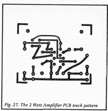
Fig. 27. The 2 Watt Amplifier PCB track pattern
6 Watt Amplifier
This simple power amplifier design gives an output power of about 6 watts RMS using a 24 volt supply and an 8 ohm impedance loudspeaker. The input impedance of the circuit is about 10 kilohms and an input level of around 225 millivolts RMS is needed in order to produce full output. However, the gain and input impedance of the circuit can both vary over wide limits with suitable changes in component values, as will be explained in more detail later.
While the output quality of the unit is not in the true hi-fi class, the total harmonic distortion is typically under 0.1% at most output powers, and the quality of the amplifier is sufficient for applications such as record players, cassette players, etc.
Due to the fairly high supply voltage required and the substantial current consumption of up to about 500 milliamps, it is not really feasible to operate the unit from a battery supply, and a mains power supply must be used.
The Circuit
A TDA2030 integrated circuit is used as the basis of this amplifier, see Figure 28, and the TDA2030 is very much like an operational amplifier having a high power class A/B output stage. It has inverting and non-inverting inputs, but unlike most audio power amplifier devices it does not have any internal biasing or feedback components.
It is possible to use the TDA2030 with a single supply or dual balanced supplies, and it can operate in the inverting and non-inverting modes. In this circuit a single supply is employed and the TDA2030 is used as a non-inverting amplifier. The circuit is really just a straight forward operational amplifier style non-inverting circuit with R1, R2 and C3 being used to effectively supply a central supply rail. The non-inverting input is biased to this by R3, and C4 provides DC blocking at the input of the amplifier. VR1 is the volume control.
R4 and R5 are the negative feedback loop and these set the closed loop voltage gain of the amplifier at approximately 30 times. C5 provides DC blocking so that R4 is effectively cut out of circuit at DC, giving unity voltage gain from the non inverting input to the output. Thus, by biasing the non-inverting input of ICI to half the supply potential the output is also biased to this voltage. This optimizes the output power that can be achieved prior to the onset of clipping and severe distortion.
C6 is the output coupling capacitor, and C1 plus C2 are supply decoupling components. D1 and D2 are protection diodes. The quiescent current consumption of the circuit is typically 40 milliamps incidentally.
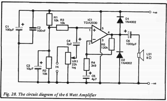
Fig 28. The circuit diagram of the 6 Watt Amplifier
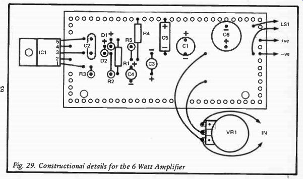
Fig. 29. Constructional details for the 6 Watt Amplifier
Within reason the voltage gain of the amplifier can be set at any desired level by giving R5 the appropriate value, and the voltage gain of the circuit is roughly equal to R5 divided by R4.
It is advisable to keep the value of R5 between about 39k and 390k since there is otherwise a risk of instability or a significant reduction in the output quality of the unit. The input impedance of the circuit can be boosted by increasing the values of R3 and VR1, but in the interests of good stability it is advisable to regard 100k and 220k respectively as the highest acceptable values.
Construction
The 6 Watt Amplifier can be assembled on a 0.1in. matrix stripboard having 13 copper strips by 29 holes using the component layout provided in Figure 29. There are no breaks in any of the copper strips. The electrolytic capacitors must be modern miniature types if they are to fit comfortably into this layout. The leadout wires of IC1 will need to be formed slightly in order to fit this device into place, and this integrated circuit has a rather unusual case style which looks rather like a plastic power transistor but with five rather than three leadout wires.
Note that IC1 must be bolted to a large heatsink such as a ready-made type rated at around 4.5 degrees Centigrade per watt. As the TDA2030 has thermal shutdown protection circuits it will probably not be damaged if it should be allowed to overheat. It would simply shut down until the temperature of the device dropped to a satisfactory level, after which it would function normally again. The TDA2030 also has output short circuit protection circuits incidentally.
The circuit has good supply ripple rejection (which can be boosted still further by increasing the value of C3 if necessary), and it is therefore unnecessary to use a well smoothed and stabilized power supply. An important point to bear in mind though is that the supply voltage under quiescent loading will be very much higher than the loaded supply potential if a non stabilized supply is used, and the supply voltage must not be allowed to exceed 36 volts (which is the maximum permissible supply potential for the TDA2030).
Components for 6 Watt Amplifier (Figure Resistors, all 1 / 4 watt 5%
R1 10k
R2 R3 10k R4 R5 120k VR1 22k log, carbon potentiometer
Capacitors
C1 100µF 40V radial
C1 electrolytic
C4 C3 10µF 25V radial electrolytic
C6 C5 4117 50V axial electrolytic
Semiconductors
IC1 TDA2030 D1 1N4002 D2 28)
10k 3k9 100nF polyester
2112 50V radial electrolytic
1000µF 25V radial electrolytic 1N4002
Miscellaneous
0.1in. matrix stripboard
Loudspeaker rated at 5 watts or more and an impedance of 8 ohms
Control knob Wire, etc.
18 Watt Bridge Amplifier
It is sometimes necessary to operate audio equipment from a supply voltage of only about 12 volts, and in-car-entertainment equipment and equipment for use in small craft are a couple of obvious examples of this. A drawback of a low supply voltage is that the maximum peak to peak output voltage swing that can be achieved (assuming a normal transformerless output stage is used) can be no more than the supply voltage, and in practice is likely to be around one to four volts less depending on the particular type of output stage employed.
Using normal 4 or 8 ohm impedance loudspeakers and a 12 volt supply this gives maximum output powers of about 4.5 watts RMS and 2.25 watts RMS respectively. This actually enables quite a reasonable volume level to be obtained, but obviously under some circumstances (such as in a noisy vehicle)
greater output power might be advantageous.
A simple way of obtaining a higher output power is to use a bridge amplifier, and Figure 30 outlines the basic arrangement of this form of amplifier. A bridge amplifier actually uses two power amplifiers with the loudspeaker connected between the outputs of the stages of amplification. One amplifier (amplifier 1 in this case) is fed with the input signal and is really just a straight forward non-inverting power amplifier. The second amplifier is a unity voltage gain inverting type and its input is fed from the output of amplifier 1.
Under quiescent conditions the outputs of both amplifier stages are at about half the supply voltage and there is no significant voltage developed across the loudspeaker. If the output of amplifier 1 goes positive, the output of amplifier 2 goes negative by an identical amount. Similarly, if the output of amplifier 1 goes negative, the output of amplifier 2 goes positive by an identical amount. Thus, if the amplifier is fully driven the outputs of the amplifiers reach virtually the full supply potentials on signal peaks, but they are out-of-phase and therefore one output is fully negative while the other is fully positive. Effectively the loudspeaker is first connected across the supply lines with one polarity, and then with the opposite polarity, and so on, giving a peak to peak output voltage equal to almost double the supply potential. Since doubling the output voltage also doubles the output current (and power is equal to current multiplied by voltage), this gives a fourfold increase in output power in comparison to an ordinary amplifier. In other words using a 12 volt supply and 4 or 8 ohm impedance loudspeakers gives maximum output powers of up to about 18 watts RMS and 9 watts RMS respectively.
The Circuit
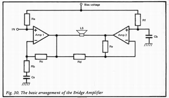
Fig. 30. The basic arrangement of the Bridge Amplifier
There are audio power ICs which are specifically designed for use in 12 volt bridge amplifier circuits, and it is also possible to use a pair of audio power amplifiers such as a couple of TDA2030 ICs. This circuit is based on an HA1388 integrated circuit which contains both the amplifiers needed to produce a 12 volt bridge amplifier, and this device has been chosen primarily because it is relatively inexpensive and seems to be readily available from a number of component retailers. It also gives excellent performance. The circuit diagram of the 18 Watt Bridge Amplifier is shown in Figure 31.
R1 and R2 form an attenuator at the input of the unit, but these are only needed if the unit is used as a booster amplifier for use with a car radio or cassette player. In this application only a very modest amount of voltage gain is needed and the voltage gain of about 40dB ( 100 times) provided by IC1 would obviously be excessive. If the unit is used in other applications where the full voltage gain is required R2 should be omitted and RI should be replaced with a link wire.
The HA1388 has internal bias and negative feedback circuits, and the only discrete components these require are four DC blocking capacitors (C3 to C6). C7 and C8 are needed to aid good stability. C9 and C10 are bootstrapping capacitors which help to optimize the efficiency and output power of the circuit.
No coupling capacitor is needed in series with the loudspeaker since there is no more than a few millivolts developed across this component under quiescent conditions. C1 is a supply decoupling capacitor and this has a fairly high value in order to additionally provide suppression of any severe noise spikes which may be present on the supply.
Construction A suitable 0.1 inch pitch stripboard component layout for the Bridge Amplifier is provided in Figure 32. Be careful not to omit the single link wire along side IC1. IC1 has an unusual 12 pin package which has the 12 pins in a single row. As the spacing of the pins is 0.1 inches this device obviously plugs into the stripboard without difficulty.
IC1 must be bolted to a large heatsink and this should preferably be rated at only about 3 degrees Centigrade per watt or less. If the unit is housed in a metal case it may well be possible to use this as the heatsink. It is acceptable for the heat tab of IC1 to connect to the negative supply rail, and it will probably be unnecessary to insulate IC1 from the heatsink or...
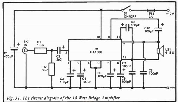
Fig. 31. The circuit diagram of the 18 Watt Bridge Amplifier
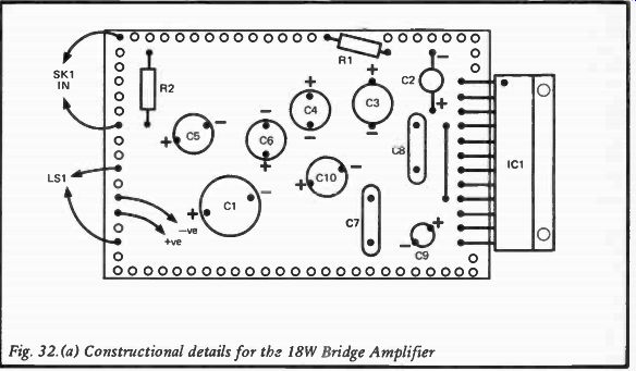
Fig. 32.(a) Constructional details for the 18W Bridge Amplifier
Fig. 32.(b) The underside of the component board
...case. However, it must not connect to the positive supply rail and insulation would therefore be needed in a positive earth set-up.
FS1 is not shown in Figure 32, but this component is an in line type.
Note that neither loudspeaker lead is at earth potential, and neither of these leads should be permitted to short circuit to earth (which would blow FS1 but would probably not do any other damage to the unit).
Components for 18 Watt Bridge Amplifier (Figure 31)
Resistors, both 1/4 watt 5%
R1 100k R2 2k7
Capacitors
C1 470µF 16V radial electrolytic C3 1002F 10V radial electrolytic C5 100,./F 10V radial electrolytic C7 100nF polyester
C9 100µF 10V radial electrolytic
C2 C4 C6 C8 C1 2µ2 50V radial electrolytic 100µF 10V radial electrolytic
- 100µF 10V radial electrolytic 100nF polyester 1004F 10V radial electrolytic
Semiconductor
IC1 HA1388
Miscellaneous
S1 SPST toggle switch FS1 3 amp in-line fuse holder and fuse
SK1 3.5mm jack
LS1 4 or 8 ohm, 10 or 20 watts RMS loudspeaker
0.1in. matrix stripboard
Case Wire, etc.
Auto Switching Unit
This unit is designed as an add-on for the previous project, and is used when the Bridge Amplifier is used as a booster amplifier for a car radio or cassette unit. The Auto Switch Unit simply switches on the booster amplifier when the radio or cassette unit is switched on, and switches the booster off again when the radio or cassette unit is turned off. This is a useful feature since it enables the unit to be mounted at any convenient point in the car, and it does not have to be positioned where it can be turned on and off easily.
The Circuit
Figure 33 shows the circuit diagram of the Auto Switching Unit. The input signal is coupled to Tri which is used as a low gain common emitter amplifier. RI is used to reduce the input impedance of the circuit and this helps to avoid spurious operation of the unit by electrical noise.
The output of Tr1 is smoothed and rectified by C3, D1 and D2, and the resultant DC bias (in the presence of an input signal from the radio or cassette unit) is used to bias the Darlington Pair (Tr2 and Tr3) into conduction. These switch on relay RLA1 and a set of normally open relay contacts are used to connect power to the booster amplifier. Of course, when the radio or cassette unit is switched off the input signal ceases, the charge on C3 decays after a few seconds, causing RLA1 and the booster amplifier to be switched off.
Construction
A suitable 0.1 inch matrix stripboard layout for the Auto Switching Unit is shown in Figure 34. The relay is not mounted on the component board, although the board could obviously be made larger in order to accommodate it if desired.
The relay used in the prototype has a 12 volt 306 ohm coil plus 8 amp changeover contacts. However, any relay having a 12 volt coil, a coil resistance of about 300 ohms or more, and at least one set of normally open contacts of adequate rating should be suitable.
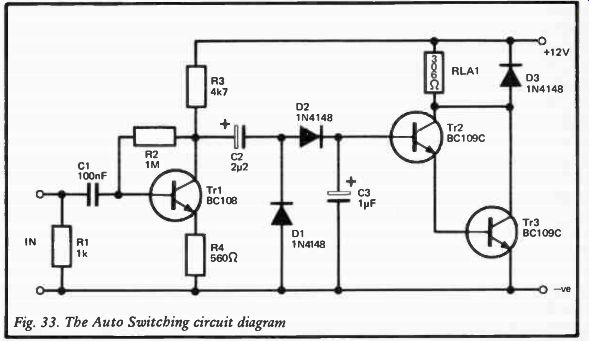
Fig. 33. The Auto Switching circuit diagram
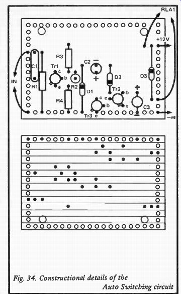
Fig. 34. Constructional details of the Auto Switching circuit
Note that power for the Audio Switching Unit should not be obtained via the relay contacts, but must be taken direct from the car supply.
Components for Auto-Switching Unit (Figure 33)
Resistors, all V4 watt 5% R1 1k R2 1M R3 4k7 R4 560 ohms
Capacitors
C1 100nF polyester
C2 2,12 50V radial
C3 le 50V radial electrolytic
electrolytic
Semiconductors
Tr1 BC108
Tr2 BC109C
Tr3 BC109C
D1 1N4148
D2 1N4148
D3 1N4148
Miscellaneous
RLA1 306 ohm 12 volt coil with 8 amp changeover contacts (or similar)
0.1in. matrix stripboard
Wire, etc.
32W + 32W MOSFET Amplifier
Integrated circuits are commonly used in power amplifiers of up to about 10 or 20 watts RMS in output power, but there are few types capable of providing higher output powers even if used in a bridge circuit, and it generally is better to use a discrete design for output powers of around 25 watts RMS or more.
Higher power audio amplifiers used to almost invariably be based on bipolar transistors, including bipolar power devices in the output stage. However, various types of power field effect device, especially power MOSFETs, have become increasingly popular in recent times. Although power MOSFETs tend to be associated with very high power and high quality designs, they are in fact perfectly practical for medium and high power applications, and where super hi-fi performance is not essential. The advantages of power MOSFETs do not significantly diminish in medium and high power applications.
Bipolar Drawbacks
While bipolar devices can be used in high performance audio power amplifiers, they do have shortcomings which have resulted in the development of superior devices such as power MOSFETs. Probably the best known drawback of bipolar devices in Class B output stages is the effect known as thermal runaway. Bipolar devices have a positive temperature coefficient and it is this that leads to thermal runaway and the possible destruction of the output transistors.
Figure 35(a) shows the basic arrangement of a conventional Class B driver and output stage, using Tr1 as a common emitter driver stage and Tr2 plus Tr3 as the complementary emitter follower output stage. The purpose of the output stage is to give current amplification (the voltage gain being only about unity) so that the circuit can provide the high output currents needed to drive a loudspeaker at high volume. Tr2 supplies the output current during positive going output excursions while Tr3 provides the output current during negative output half cycles.
The main collector load for the driver transistor is formed by a constant current source, and this gives improved linearity in comparison to results obtained using a straight forward load resistor. This is due to the variations in gain (and consequent distortion) that result when a transistor operates over a wide range of collector currents. Using a load resistor in a common emitter stage which has a large output voltage swing inevitably results in a very wide collector current range and substantial distortion. The use of a constant current load does not totally eliminate distortion since the collector voltage does obviously vary, and the gain of a transistor is to a certain extent dependent on collector voltage. However, as changes in gain due to variations in collector voltage are relatively small, low distortion levels of only a fraction of one percent can be readily achieved.
The bias circuit between the bases of the output transistors
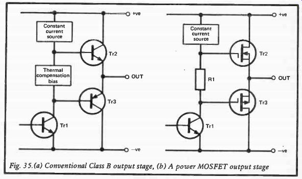
Fig. 35
is needed to bring the output transistors to the point where they are just conducting. If this is not done, small variations in the collector voltage of Tr1 would fail to bring the output devices into conduction and would not give any change in output voltage! Higher voltage swings at Tr1's collector would give a change in output potential, but the initial and final part of each half cycle would be missing, giving severe "crossover distortion" as it is termed.
Unfortunately, bringing the output devices to the threshold of conduction does not totally eliminate crossover distortion because the output devices exhibit comparatively low levels of gain when operating at low collector currents. This gives a mild but unacceptable form of crossover distortion. Negative feed back can be used to combat crossover distortion of course, but in order to obtain really good results it is nevertheless necessary to use a fairly high quiescent bias through the output transistors It is this substantial bias current that leads to problems with thermal runaway. The bias current tends to heat the output transistors, and due to their positive temperature coefficient this gives a rise in bias current. This produces increased heat and a consequent further increase in bias current. This positive feedback therefore gives a steady rise in bias until the output transistors become overheated and are destroyed.
In order to prevent this the bias circuit is made temperature sensitive, and is designed to reduce the bias if increased temperature is sensed. Thus, as the output transistor heat up the bias circuit is affected by the heat that is generated and prevents any increase in the bias current. In practice the bias stabilization will not be perfect and some fluctuation will occur, but a well designed circuit will have more than adequate bias stability.
Power MOSFETs Like bipolar transistors, when used in a Class B output stage power MOSFETs require a forward bias to minimize crossover distortion. However, as power MOSFETs have a negative temperature coefficient at currents of around 100 milliamps or more (and a mild positive temperature coefficient at low current it is possible to use a simpler Class B driver and output stage, as shown in Figure 35(b). The temperature stabilized bias circuit can be replaced with a resistor since the temperature characteristics of power MOSFETs gives built in stabilization of the bias current at about 100 milliamps (which is about the optimum bias current).
Another problem encountered with bipolar power devices is that of relatively low current gains of typically only around 20 to 50. This is inadequate for medium and high power amplifiers since it would require an excessively powerful driver stage. The normal way around this problem is to use Darlington Pairs or some similar arrangement to give a sufficiently high current gain to permit the use of a low power driver stage.
Power MOSFETs, like all FET devices, are voltage rather than current operated. The input impedance of power MOSFET devices is so high that no significant input current is drawn at low operating frequencies, but at high operating frequencies the input impedance is much lower due to the rather high input capacitance of around 500 picofarads. Despite this input capacitance an operating current of only about 10 milliamps through the driver stage is sufficient, even though the peak output current could be as much as a thousand times this figure.
A further drawback of bipolar power devices is their relatively slow switching time. This can produce a number of problems, including slewing induced distortion. This is where a strong high frequency signal may demand a change in output voltage of (say) 2 volts per microsecond, whereas the output stage might nave a slew rate of perhaps just one volt per microsecond, obviously the output will be unable to give a faithful reproduction of the input signal and distortion inevitably results. An inadequate slew rate can also give an amplifier a poor power bandwidth, with the maximum available output power falling considerably at high audio frequencies.
A further problem is the phase lag which occurs through the output stage at high frequencies, and which can result in the feedback through the negative feedback network becoming positive rather than negative at very high frequencies. If the amplifier has sufficient gain at these frequencies the amplifier will oscillate, and instability will still be evident even if the gain of the circuit is not quite sufficient to produce oscillation.
This can be overcome by including components to roll-off the high frequency response of the circuit, and by including phase compensation components. This reduces the performance of the amplifier at high audio frequencies though.
Power MOSFETs have a switching time that is typically about 50 to 100 times faster than a bipolar power transistor, and problems with poor high frequency performance are thus largely overcome by the use of these devices. It is in fact possible to produce designs which have no frequency or phase compensation components but still possess good stability, and have a level of performance which is maintained to frequencies well beyond the upper audio limit.
Another problem encountered with bipolar power transistors is that of secondary breakdown. This is a sort of localized thermal runaway which produces a "hot spot" on the chip with a consequent short circuit between the collector and emitter terminals. This has to be avoided by only operating the transistor within certain combinations of collector current and voltage. In audio amplifier circuits this often means that the output transistors are operated well within their thermal limitations, and the maximum output power available from a given set of output transistors is often far less than their maximum dissipation figures would suggest.
Due to their negative temperature coefficient at high drain currents power MOSFETs do not suffer from secondary breakdown and the maximum drain current and drain voltage combinations that can be used are virtually only limited by the thermal dissipation capabilities of the devices. They are therefore eminently suitable for use in high power audio amplifiers.
MOSFET Disadvantages
While MOSFET power devices are not without drawbacks, these are relatively few and minor. Originally they were very much more expensive than bipolar transistors of comparable power rating, but the price difference is very much smaller these days.
When one takes into account the fact that the use of power MOSFETs allows more simple circuitry to be used with a consequent indirect saving in cost, it is probable that bipolar transistors no longer have a significant cost advantage.
Power MOSFETs tend to have higher open loop distortion than bipolar devices, but the high gain and fast switching speed of power MOSFETs enables a high level of negative feedback to be used over the entire audio band, giving unsurpassed closed loop distortion performance.
Another drawback is that power MOSFETs tend to be rather less efficient than bipolar devices when used in conventional Class B output stages. This is simply because a high power emitter follower stage produces a voltage drop of up to about one volt or so between tie input and output, whereas there is a drop of a few volts from the input to the output of a source follower stage. There is no easy way around this problem, but a slight reduction in efficiency is not really a major drawback anyway.
Practical Circuit
Figure 36 shows the circuit diagram of a practical 32 watt plus 32 watt power MOSFET amplifier, and apart from the use of MOSFETs in the output stage this is basically a quite conventional design.
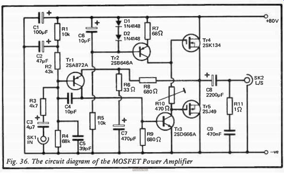
Figure 36
Tr1 is a common emitter input stage, and is direct coupled to common emitter driver stage Tr3. These two stages provide all the amplifier's voltage gain, and have a very high combined gain. Tr2 and its associated components form a straight forward constant current generator having a nominal output current of 10 milliamps, and this forms the main collector load for Tr3.
R10 is used to set the appropriate quiescent bias current through the output transistors, and as explained earlier, the thermal stabilization of the bias current is not achieved in the bias circuit, but is instead provided by the output devices themselves.
R8 provides almost 100% negative feedback from the output of the amplifier to the emitter. of Tr1, giving the circuit only about unity voltage gain at DC. R1, R2 and R4 are used as a potential divider which biases the input of the amplifier, and therefore the output as well, to approximately half the supply voltage. This permits the maximum possible output level prior to clipping and the commencement of serious distortion. R1 and C2 form a smoothing circuit which prevents hum and other noise on the supply lines from being coupled to the input of the amplifier through the bias circuit.
R3 and C5 form an RF filter which helps to avoid problems with RF signals breaking through to the output and producing audible signals. C4 also helps in this respect by rolling-off the high frequency response of the amplifier, well above the upper audio limit.
In order to give the amplifier a useful voltage pin at audio frequencies it is necessary to decouple some of the negative feedback. C7 is the decoupling capacitor and R6 is used to limit the amount of feedback that is removed. The voltage gain of the circuit is roughly equal to R8 divided by R6, or about 20 times (26dB) with the specified values. The maximum output voltage of the amplifier is 16 volts RMS, and this gives an input sensitivity of approximately 777 mV RMS for full output. The input impedance is over 20k.
C3 and C8 are the input and output coupling capacitors respectively while C1 provides supply decoupling. R11 and C9 are the only components required to aid stability, and these form the familiar Zobel network that is normally included across the output of semiconductor power amplifiers.
Performance The prototype amplifier seems to work extremely well, especially when one takes into account the relative simplicity of the unit.
The circuit will comfortably give 32 watts RMS into an 8 ohm load, and the total harmonic distortion is only about 0.05% or less for any power level up to this figure. Measurements on the prototype were only made at 1kHz, but the open loop gain of the circuit is virtually constant over the audio frequency range, and the distortion performance should be as well. The closed loop frequency response of the circuit has -2dB points at approximately 20Hz and 22kHz. The signal to noise ratio of the circuit (unweighted) is in excess of 80dB, although in practice there is likely to be a small amount of mains hum from the power supply to add to the noise generated by the amplifier and this figure may not quite be realised.
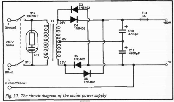
Fig 37. The circuit diagram of the mains power supply
Power Supply
Figure 37 shows the circuit diagram of a suitable power supply for the 32 watt plus 32 watt MOSFET amplifier, and this is sufficient to power a mono or a stereo version of the amplifier.
The circuit is effectively two push-pull rectifier and smoothing circuits having their outputs connected in series to give a total output voltage equal to double the potential given by a single rectifier and smoothing circuit. D4, D6 and C10 form one section of the unit while the other is formed by D3, D5 and C11.
These each give a little under 40 volts under no load, and a combined unloaded output potential of just under 80 volts.
This drops to about 77 volts when loaded by a stereo amplifier under quiescent conditions, and to only about 60 volts or so when powering a stereo amplifier with both channels being run at high power.
S1 is the on/off switch and LP1 is the on/off indicator. It is essential that the latter is a type having a built-in series resistor for use on the 240 volt U.K. mains supply.
The mains transformer used in the prototype has a rating of 26 - O - 26 volts at 3.5 amps, but it is not essential to use a component having precisely these ratings. A 25 - O - 25 volt type rated at about 4 amps or more should be equally suitable.
Do not use a type having a secondary voltage rating of more than 26 volts as this could result in the unloaded or quiescent loaded supply voltage being higher than the 40 volt rating of smoothing capacitors C10 and C11.
Construction A suitable printed circuit board design for the 32 watt MOSFET amplifier is shown in Figure 38 (the component layout) and Figure 39 (the track pattern). This is for a single amplifier and obviously two boards must be constructed if a stereo amplifier is required.
Figure 37 shows the circuit diagram of a suitable power supply
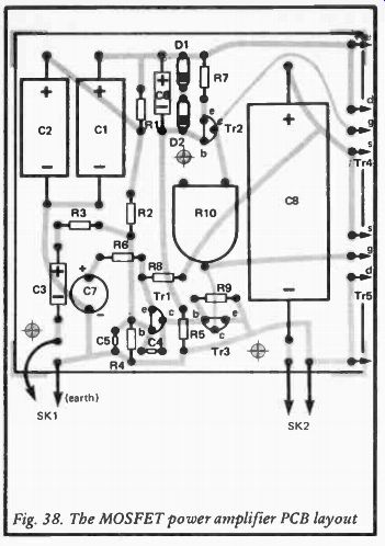
Fig. 38. The MOSFET power amplifier PCB layout
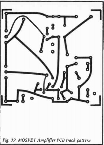
Fig. 39. .140SFET Amplifier PCB track pattern
The output transistors are not mounted on the board, but are fitted on a large heatsink, and a "Redpoint" type 4Y heatsink (which is a 4.5 degree Centigrade per watt type) was used in the prototype. This can be obtained ready drilled to take two TO-3 style power transistors (such as the output devices used in this design) or it can be obtained undrilled. If you drill the heatsinks yourself a TO-3 size mica insulating washer can be used as a template when marking out the positions of the mounting holes. It is not essential to insulate the transistors from the heatsink since the sources of the transistors connect to their metal cases, and the sources of the transistors must connect to each other anyway. If they are not insulated from the heatsink it is clearly necessary to prevent the heatsinks from coming into electrical contact with other parts of the circuit, and in a stereo circuit the separate heatsinks for the two amplifiers must not be allowed to come into electrical contact with one another.
It is important to use quite short leads of no more than about 50mm in length to connect the output transistors to the printed circuit board, and this is particularly important in the case of the leads which connect to the gate terminals of the output devices.
Due to the high gain of the power MOSFETs at high frequencies long leads could result in poor stability or even RF oscillation and damage to the output transistors. However, in practice there should be no difficulty in arranging the layout of the unit so that these leads are suitably short.
Note that C9 and R11 are not mounted on the printed circuit board but are simply wired in series across the output socket. A screened input cable should be used.
Power Supply Construction
The power supply circuitry is constructed using point to point style wiring, as shown in Figure 40. This is quite straight forward but assumes that C10 and C11 are both types having a dummy tag. If they are not it will be necessary to use a tagstrip to provide a couple of connection points. A solder-tag is fitted to one of the mounting bolts of Tl, and this provides a chassis connection point for the mains earth lead.
Adjustment It is essential to thoroughly check the wiring before switching the unit on since wiring errors could result in expensive damage, and could conceivably be dangerous. Before switching on it is essential to adjust R10 for minimum resistance (set in a fully anticlockwise direction). With FS1 temporarily removed and a multimeter set to read 500mA FSD connected across the fuse holder, a reading of approximately 20mA should be obtained when the unit is turned on (or 40mA for a stereo unit). If the reading is considerably different to this switch off at once and recheck the wiring.
If all is well, advance R10 to increase the meter reading to about 100mA. For a stereo unit R10 in one channel should be adjusted to bring the current consumption up to 120mA, after which R10 in the second channel should be adjusted to raise the current consumption to 200mA. The amplifier is then ready for use.
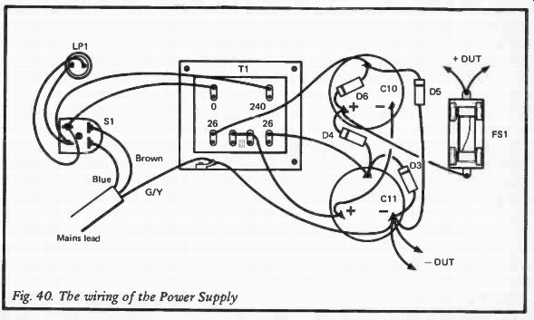
Fig. 40
Be careful not to touch any of the mains connections when making adjustments and measurements on the unit, and exposed wiring or connections at the mains potential must be well insulated before connecting the unit to the mains supply. Of course, as with any mains powered project the unit must be housed in a case which can only be opened with the aid of a screwdriver or other tool so that there is no easy way to gain access to the dangerous mains wiring and accidents are avoided. Any exposed metalwork should be earthed to the mains earth lead in the interest of safety.
Components for 32 Watt MOSFET Amplifier (Figure 36)
Resistors, all 1/4 watt 5% except R10
R1 R3 R5 R7 R9 R11 10k 4k7 10k 68 ohms 680 ohms 1 ohm
R2 43k R4 68k R6 33 ohms R8 680 ohms
R10 470 ohms 0.25 watt horizontal preset
Capacitors
C1 100 uF 100V axial C2 electrolytic C3 447 63V axial C4 electrolytic C6 C5 39pF ceramic plate C7 470µF 63V radial
C8 electrolytic C9 470nF polyester 47 uF 100V axial electrolytic 10pF ceramic plate 10µF 25V axial electrolytic 2200µF 63V axial electrolytic
Semiconductors
Tr1 2SA872A Tr2 Tr3 2SD666A Tr4 Tr5 2SJ49 D1 1N4148 D2 2SB646A 2SK134 1N4148
Miscellaneous
SKI Phono socket SK2 Printed circuit board Heatsink Wire, etc.
2 way DIN type
Components for MOSFET Amplifier Power Supply (Figure 37)
Capacitors
C10 4700µF 40V tag ended
C11 4700µF 40V tag ended electrolytic, electrolytic
Semiconductors
D3 1N5402 D4 1N5402 D5 1N5402 D6 1N5402
Miscellaneous
T1 Standard mains primary, 26 - O - 26 volt 3.5 amp secondary or similar LPI Panel neon indicator with integral series resistor for 240V main use FS 13 amp 20mm quick blow and chassis mounting holder Si Rotary mains on/off switch Control knob Mounting clips for C10 and C11 Wire, etc.
100W MOSFET Amplifier
Depending on the power supply used, this amplifier will give an output power of between about 50 and 100 watts RMS into an 8 ohm impedance load. Like the previous circuit it uses MOSFET power transistors in the output stage to give a high level of performance despite the relative simplicity of the circuit.
The total harmonic distortion of the circuit is less than 0.05% provided the circuit is not overdriven, and the signal to noise ratio is better than 100dB.
The Circuit
This circuit is based on a Hitachi design, and Figure 41 shows the full circuit diagram of the unit. Unlike the previous circuit, this one uses DC coupling to the loudspeaker and has dual balanced supplies with a central OV and earth rail. This eliminates the need for a large output coupling capacitor plus the reduction in low frequency performance that this capacitor produces, and it also helps to give the circuit good supply ripple rejection.
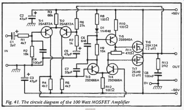
Fig. 41. The circuit diagram of the 100 Watt MOSFET Amplifier
Apart from the DC coupling, the configuration used in this circuit is quite different to that employed in the previous design.
The input and driver stages of the unit both use differential amplifiers. The input stage uses Tri and Tr2 while the driver stage is based on Tr3 and Tr4. Tr5 forms a constant current collector load for Tr4. The signal path through the amplifier starts with input coupling capacitor C1, and RF filter R1 - C4.
R2 biases the input of the amplifier to the central 0V supply rail. Tri is effectively a common emitter amplifier with its output direct coupled to Tr4 which is used as a common emitter driver stage. From here the signal is coupled to Tr6 and Tr7 which are the complementary source follower output stage.
Negative feedback is taken from the output of the amplifier to the base of Tr2, and although there is no inversion of the signal from the base of Tri to the output of the unit, there is an inversion from the base of Tr2 to the output. This is due to Tr2 effectively acting as an emitter follower which drives the emitter of Tr1. With an input signal to the emitter of Tri this device effectively operates as a common base stage. Thus there is no inversion through Tri and Tr2, there is an inversion through Tr4, and there is no phase change through the output stage, so that the output of the amplifier and the base of Tr2 are out-of-phase and the required negative feedback is obtained.
The values given to R6 and R7 give a voltage gain of about 28 times.
As was mentioned earlier, a slight drawback of power MOSFETs is that they are less efficient than bipolar transistors when used in a conventional Class 13 output stage, and their relative efficiency becomes somewhat worse in high power circuits where the high source currents require a gate to source voltage of several volts. The maximum output voltage swing is equal to the supply voltage less the maximum gate to source voltage of each transistor (if other more minor factors are ignored), and this obviously gives an output voltage swing which is far less than the supply voltage used.
A simple way of obtaining better efficiency is to simply use two identical devices connected in parallel for each output transistor. The maximum current handled by each output transistor is then approximately halved, and the maximum source to gate voltage of each device is reduced accordingly (with a corresponding increase in the output voltage swing of the amplifier). This method can produce problems if tried with bipolar devices, and this is largely due to the positive temperature coefficient of these devices. If one output transistor tends to draw more current than the other (which is almost certain since the devices are not likely to be perfectly matched), one device becomes hotter than the other. This higher temperature results in the emitter - base threshold voltage of the transistor being reduced, and it consequently draws an even larger share of the output current. The device then becomes hotter, and this process continues until one output transistor is taking most of the output current while the other is largely ineffective.
This problem does not arise with power MOSFET transistors due to their negative temperature coefficient. If one device draws a higher output current than the other, the increase in its temperature causes an increase in the source to gate voltage needed for a given source current, and this device's share of the output current diminishes. In other words, rather than a tendency for the mismatch to be accentuated, the negative temperature coefficient has a stabilizing effect. This makes it possible and completely safe to simply wire two power MOSFE1 in parallel without using any additional components to ensure accurate sharing of the output current.
Power Supply
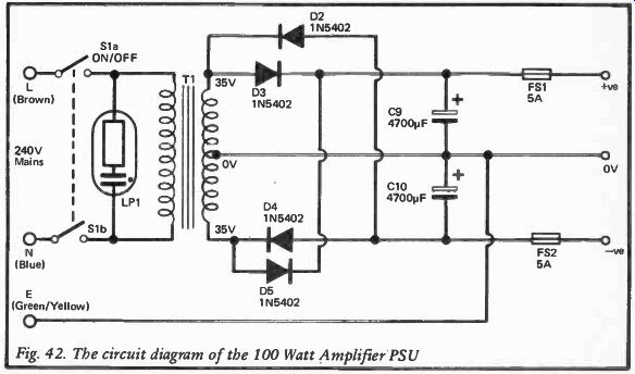
Figure 42.
A suitable power supply circuit for the 100 watt MOSFET amplifier is given in Figure 42.
This is very similar to the power supply circuit for the previous amplifier, but the center tap on the supply at the junction of the two smoothing capacitors was formerly ignored.
In this case this is used to give the central OV earth supply, and the mains earth connects to this point in the circuit rather than to the negative supply rail. Fuses are included in both the positive and negative rails, of course.
The power obtained from the amplifier depends on the mains transformer used in the Ti position. For most purposes a 35 - 0 - 35 volt 160VA toroidal mains transformer should suffice. For stereo operation either a transformer of the same voltage rating but a 300VA type should be used, or a separate supply using a 160VA component could be used for each channel. This gives a supply voltage of around 50 volts under quiescent conditions, but at full load the supply voltage falls substantially. This permits an output of up to about 70 watts RMS to be obtained using 8 ohm impedance loudspeakers.
Increased output power can be obtained by either using a mains transformer having a higher power rating, or one having a slightly higher secondary voltage, or a combination of the two.
Using a 40 - 0 - 40 volt 300VA transformer (or a 500VA type for stereo operation) gives a supply potential of approximately ± 60 volts under quiescent conditions, and although the supply potential reduces somewhat at full load, the amplifier is nevertheless capable of comfortably providing 100 watts RMS into an 8 ohm impedance load. The use of a transformer having a voltage rating of more than 40 - O - 40 volts is not recommend An important point to note is that the 1N5402 rectifiers used in this circuit have a maximum current rating of 3 amps.
This is sufficient for a single amplifier, but is inadequate for a stereo type. For stereo operation either a separate supply for each channel should be used, or the rectifiers must be replaced with higher power types. Individual rectifiers of suitable current rating do not seem to be readily available, but a bridge rectifier could be used instead. Any type having a voltage rating of 200 volts or more and a current rating of about 6 amps or more should be suitable.
Construction
A suitable printed circuit design for the 100 watt MOSFET amplifier is shown in Figures 43 and 44. The four output transistors must be mounted on a large heatsink, and in the prototype a "Redpoint" type 4Y (4.5 degree Centigrade per watt) heatsink was used for each pair of output devices. Do not use heatsinks rated at less than 4.5 degree Centigrade per watt, and if a single heatsink is used for all four transistors it must obviously be a very large type rated at about 2 degrees C per watt or less.
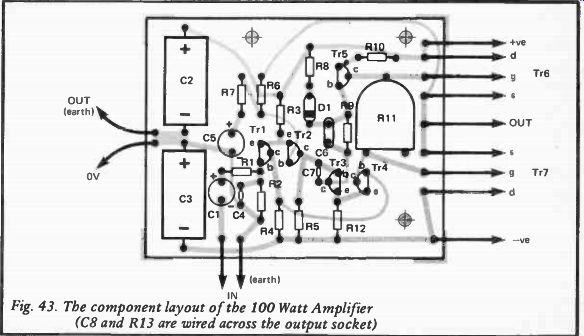
Fig. 43. The component layout of the 100 Watt Amplifier (C8 and R13 are wired
across the output socket)
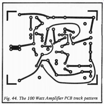
Fig. 44. The 100 Watt Amplifier PCB track pattern
The leads to the output transistors should be quite short, and preferably no more than about 50 mm long. If they do need to be a little longer than this a low value resistor (about 68 ohms) can be added in the gate circuit of each output transistor. In conjunction with the input capacitance of each output device these resistors form simple lowpass filters which reduce the RF performance of the amplifier and helps to avoid high frequency instability. The performance of the amplifier at high audio frequencies would only be marginally affected by the addition of these resistors, and it is highly unlikely that they would introduce any discernable reduction in the reproduction quality.
The two transistors which form Tr6 are wired in parallel, with the two drain terminals being connected together, the two gate terminals wired together, and the two source terminals connected to each other. The two devices which form Tr7 are connected together in the same way. Note that C8 and R13 are wired across the output socket and are not included on the PCB design.
Probably the best method of construction to use for the power supply is straight forward hard-wiring, as for the power supply for the previous amplifier. The wiring is much the same as for this previous circuit (see Figure 40 for the wiring diagram), but the chassis and mains earth lead connect to the junction of the two smoothing capacitors (C9- and C10+), and the 0V supply output is taken from here. The only other change is that a fuse is included in the negative output of the unit as well as in the positive output.
The printed circuit design includes earth connection points for the input and output of the unit, and satisfactory results should be obtained using these. However, slightly better results may be obtained if the input and output earth connections are taken from the power supply at the take-off point for the 0V supply for the amplifier.
Incidentally, the type numbers of the transistors used in this and the previous amplifier design may seem a little unusual, but they are in fact Japanese type numbers and the specified devices are available from a few suppliers. The 2SB716 and 2SD756 are suitable alternatives for the 2SB646 and 2SD666 devices.
Adjustment
Before switching on the completed amplifier thoroughly check all the wiring a couple of times. In particular check the power supply wiring and the connections to the output transistors.
Mistakes here could easily result in damage to the unit, and some of the more expensive components in the unit are amongst those which are most at risk. Start with R11 set in an almost fully counter-clockwise direction, and do not initially connect a loudspeaker to the output of the unit. Instead, connect a multimeter set to read a few volts (DC) FSD across the output to check that a low quiescent output voltage is present. Only a small fraction of a volt should be detectable, or possibly no DC voltage at all will be found. If a significant DC voltage is detected switch off the amplifier at once and recheck the wiring.
If all is well, connect a loudspeaker to the unit and give it an initial check. As for the previous design, R11 is adjusted for an increase in quiescent current consumption of about 100 milliamps. The current meter can be used to monitor either the positive or the negative supply when adjusting R11.
The amplifier requires an input of about one volt RMS in order to produce full output, and the input impedance is about 18 kilohms. The use of loudspeakers having an impedance of less than 8 ohms is not recommended.
Components for 100 Watt MOSFET Amplifier (Figure 41)
Resistors, 14 watt 5% except where noted
R1 4k7 R2 R3 68k
R4 R5 4k7 R6 R7 1-k R8 R9 15k 1/2 watt
R10 R11 470 ohms 0.25 watt R12
horizontal preset R13 2R2
Capacitors
C1 2u2 63V radial C2 electrolytic C3 47 uF 63V axial C4 electrolytic C6 47µF 10V radial C8 electrolytic 33pF ceramic plate C5 C7
47µF 63V axial electrolytic 100pF ceramic plate 6n8 mylar
100nF polyester
Semiconductors
Tr1 2SA872A Tr3 Tr5 Tr1
D1 2SD666A 2SB646A 2SJ49 (2 off)
1N4148
Miscellaneous
Printed circuit board Heatsinks
Tr2 Tr4 Tr6 18k 4k7 27k 100 ohms 100 ohms 100 ohms
2SA872A 2SD666A 2SK134 (2 off)
Input and output sockets Wire, etc.
Components for 100W Amp. Power Supply Unit (Figure 42)
Capacitors C9 4700µF 63V tag C10 4700µF 63V tag ended electrolytic ended electrolytic Semiconductors D2 1N5402 D3 1N5402 D4 1N5402 D5 1N5402 Switch S1 Rotary mains switch (See Text)
Transformer
T1 35 - O - 35 volt 300VA toroidal mains transformer (see text)
Miscellaneous
FS1 20mm quick-blow 5 amp fuse FS2 20mm quick-blow 5 amp fuse
LP1
Panel mains indicator with integral series resistor for mains use.
Chassis mounting fuseholders for FS1 and FS2, control knob, mains lead, wire, etc.
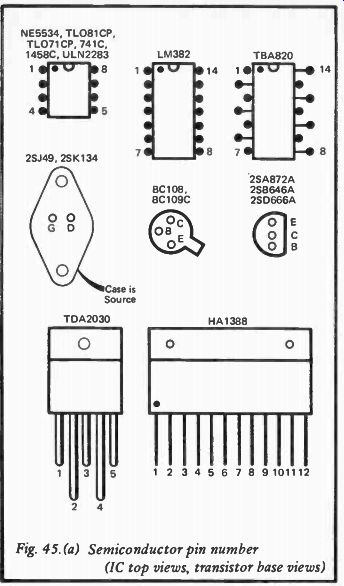
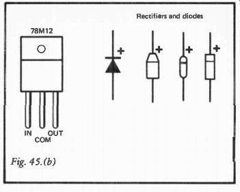
Fig. 45.(a) Semiconductor pin number (IC top views, transistor base views)
Fig. 45.(b)
Prev: PRE-AMPLIFIERS
Also see:
Using Scopes in Transistor Circuits (1968)
Practical TRANSISTOR Servicing (1967)
Principles Of Transistor Circuits [1959]