BY JOHN ROBERTS
Analog system employs a bucket-brigade device and compansion to provide adjustable delays and wide dynamic range.

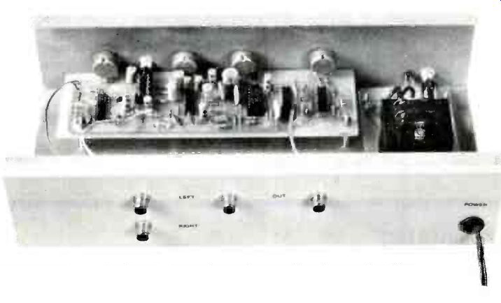
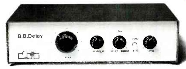
--------- Photograph of the author's prototype. The large control knob adjusts vco frequency and, hence, delay time.
-------THE AUDIO BUFF is constantly seeking ways to make the sound from his audio system more realistic. That's why there's been a high level of interest in a family of audio components known as audio delay lines or "room expanders." Such a component is intended to create an auditory illusion that simulates the environment in which music is ordinarily performed-a large concert hall, a night club, etc. rather than the sense of being reproduced in a small listening room. To provide you with a component that will achieve this objective with any hi-fi system, we present here an analog audio delay line, that can be built by a technically inclined audiophile for a relatively moderate cost. The delay line described is analog in design.
---------
THE analog audio delay line described here employs a high-performance, "bucket-brigade" analog shift register and a 2:1 compansion system to preserve as much of the input signal's dynamic range as possible. According to its designer, it offers an adjustable delay time of from 5 to 68 ms, a frequency response of 30 to 12,000 Hz (+0,-1 dB), an output noise rating ("A" weighted) of -91.5 dBm at 5-ms delay, and a THD + N content of 1% at kHz. A complete stereo delay-line kit including an ac or dc power supply and a custom enclosure is available for $250. Delay Lines and Reverberation. Perhaps the most significant difference between a large concert hall and the typical home listening room lies in their reverberation times. Reverberation time can be defined as the amount of time it takes for a steady-state sound field to decay to-60 dB relative to the level that existed before the sound source was deactivated. The size of a room and the materials used to construct it affect its reverberation time.
Because the speed of sound in air is relatively constant (approximately one foot or 0.3 meter per millisecond) for given atmospheric conditions, sound waves travelling in a very large room will experience fewer energy-absorbing collisions with the walls, floors, and ceiling per unit time than will similar sound waves travelling in a small room. Accordingly, sound waves in the large room decay less rapidly.
A listener in a reflective room receives a series of sound waves starting with the wave that reaches him on a direct path from the source. The reflected waves arrive at some time after the direct signal. The human ear derives from these differences in arrival times clues as to the size of the listening space.
When the reflections arrive so soon after the direct wave that they merge with it, the room "sounds" small. By contrast, larger differences in arrival times and more protracted reverberation tell the listener that he is in a large hall.
In operation, an audio delay line accepts signals from the main audio channels, stores them for a given amount of time, and then presents them to a power amplifier which drives one or more speaker systems. The speakers driven by the main-channel signals are placed in front of the listener, and the speaker(s) driven by the delayed information is (are) placed behind him or off to the sides. The goal is to synthesize the reverberative characteristics of the type of environment in which the recorded program material would ordinarily be performed.
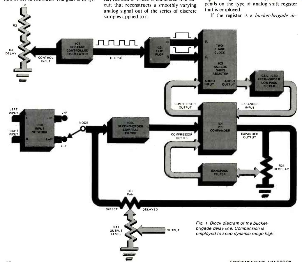
Fig. 1. Block diagram of the bucket-brigade delay line. Compansion
is employed to keep dynamic range high.
Delaying the Signal. Various means, electromechanical and electronic, are available for providing delayed signals; but cost, complexity, and space requirements make most of these impractical for use in the home. It seems fair to say that use of delayed signals to enhance home music reproduction was brought about by the availability of purely electronic delay systems.
State-of-the-art reverberation synthesizers derive suitable audio delays by means of analog or digital shift registers. In either method, the audio signal is divided at a given rate into samples that describe its instantaneous amplitude. These are sequentially deposited in a shift register that stores them for a given amount of time.
The samples are clocked through the register, the end of which is connected to a circuit that reconstructs a smoothly varying analog signal out of the series of discrete samples applied to it.
The difference between analog and digital delay lines lies in the manner in which the input signal is sampled, stored, and reconstructed. In an analog system, the input signal is sampled and its instantaneous amplitude is applied to the input of an analog shift register. What happens next depends on the type of analog shift register that is employed.
If the register is a bucket-brigade de-vice, the sampled voltage charges a small input capacitor. This charge is then transferred to the first of a long series of storage capacitors by means of a voltage-controlled switch ( a FET driven by one component of a two-phase clock). Next, a new sample charges the input capacitor and the first sample is transferred to the second in the string of storage capacitors. The sample in the input capacitor is then transferred to the first storage capacitor; the input capacitor receives a new sample; the sample in the second storage capacitor is transferred to the third while that in the first is transferred to the second; and so on.
This process goes on continuously and the analog samples of the input waveform make their way down the bucket-brigade device in the form of packets of charge being shifted from one capacitor to the next. At the end of the register, a low-pass filter integrates the staccato sequence of samples delivered to it into a smoothly varying replica of the input waveform.
The second type of analog shift register, the charge-coupled device, functions in a similar manner but employs a different method of storing and transferring the analog samples of the input waveform. Instead of using actual capacitors to store the charge packets, a charge-coupled device or CCD employs the equivalent capacitances of a series of MOSFET channels which form under gate structures biased by voltages greater than the MOS threshold.
The MOS elements of a CCD are close enough to each other that the free charge consisting of minority carriers stored in the inversion layer associated with one MOS capacitor (the channel) can be transferred to the channel region of the adjacent device. The transfer of charge is governed by the multi-phase clock voltages applied to the gate structures of adjacent MOS devices. In a CCD, an analog sample of the input signal is stored as a channel charge.
Because CCD gates are very small (typically a few square micrometers in area), tiny amounts of charge are involved--usually from approximately 10 electrons (!) to 10' electrons.
In an analog delay line, the amount of delay that is obtainable depends on both the rate at which the samples are clocked through the shift register and the number of storage elements in the register. Current IC fabrication techniques have made possible the construction of BBD or CCD delay lines containing hundreds and even thousands of storage elements. Such devices offer delays as long as 100 milliseconds or more-longer than necessary for most reverberation synthesis applications.
The faster the clock frequency, the shorter the delay and, for a given device, the more closely the output signal resembles the input signal. As a rule, longer delays result in some loss of high frequencies and degradation of dynamic range.
Advanced delay-line ICs offer impressive performance in spite of these limitations.
For example, the Reticon SAD-4096 employed in the project to be described here has 2048 storage elements, a clock-frequency range of 8 kHz to 2 MHz, and a delay range of 1 millisecond (2-MHz clock) to 250 milliseconds (8-kHz clock). The dynamic range of its output is 65 dB when the clock frequency is a relatively low 20 kHz. The use of compansion can provide even greater dynamic range.
In a digital system, the input waveform is sampled at an appropriate rate. Each sample is applied to an A/D converter which transforms it into a sequence of bits describing its instantaneous amplitude in digital form. Each digital word describes a specific sample and is applied to either a digital shift register or to a RAM, depending on the design of the delay line. If a shift register is employed, the words are clocked through the register at a specific clock rate and eventually appear at its output. If a RAM is used, the words are written into specific memory locations, stored in them for a certain period of time, and then read out of the memory locations in the appropriate order.
As the digital words stream out of the register or are read out of the RAM, they are applied to the input of a D/A converter which changes them back into analog form. Low-pass filtering smooths out the reconstructed analog waveform. The total delay provided by a digital system depends on the length of the shift register and the rate at which data is clocked through it or on the size of the RAM and the rate at which digital data is written into and read out of it.
Some delay line designs employ delta modulation. That is, the input waveform is sampled continuously and compared to the previous sample. The circuit that processes the input waveform generates an output signal that describes the result of this comparison-whether the input signal has decreased or increased in amplitude, or remained constant. If this is done, only "change" information need be clocked through a register or written into memory, rather than information completely describing the instantaneous amplitude of the input signal at each moment that it is sampled. At the output of the storage circuit, a demodulator reconstructs an analog replica of the input waveform that is low-pass filtered to remove abrupt level changes introduced by the delta modulator.
--------------------
PARTS LIST
DELAY CIRCUIT
C1, C18, C19, C32—0.1-µF, 50-V disc ceramic capacitor
C2-100-µF, 16-V radial-lead electrolytic
C3, C13, C16, C25, C27—4.7-µF, 16-V radial-lead electrolytic
C4--0.01-µF, 5% Mylar capacitor
C5, C11, C21, C22, C24--100-pF, 5°/o polystyrene capacitor
C6, C7, C8, C12, C17--1-µF, 25-V radial-lead electrolytic
C9, C14--5-pF, 50-V disc ceramic capacitor
C10--2200-pF, 5% polystyrene capacitor
C15, C26--0.47-µF, 25-volt radial-lead electrolytic
C20--1000-pF, 5°/o polystyrene capacitor
C23--510-pF, 5% polystyrene capacitor
C28--0.0022-µF, 5% Mylar capacitor
C29, C30--470-pF, 50-V disc ceramic capacitor
D1, D2--1N914 diode
IC1-CD4007AE dual complementary pair plus inverter
IC2-CD4013AE dual D flip-flop
IC3--SAD-4096 bucket-brigade analog shift register (Reticon)
IC4--NE570N compander
IC5--TL074CN quad BiFET op amp
J1, J2, J3, J4-phono jacks
The following, unless otherwise specified, are 1/4-watt, 5%, fixed carbon-composition resistors.
R1, R6, R7-1000 ohms
R2, R10 through R15, R22, R31, R32, R34-100,000 ohms
R3, R36, R41-100,000-ohm, linear-taper potentiometer
R4, R25, R26-3300 ohms
R5--300,000 ohms
R8, R40--100 ohms
R9--75,000 ohms
R16, R17-22,000 ohms
R18, R35-68,000 ohms
R19, R20, R37, R38-43,000 ohms
R21-10 ohms R23-36,000 ohms
R24, R27, R28-15,000 ohms R29-62,000 ohms
R30-180,000 ohms
R33-20,000 ohms
R39-10,000-ohm, linear-taper potentiometer
S1-Dpdt pc-mount push-on / push-off switch
Misc.--Printed circuit board, IC sockets or Molex Soldercons, circuit board standoffs, control knobs, suitable enclosure, shielded patch cords, hookup wire, etc.
---------------------
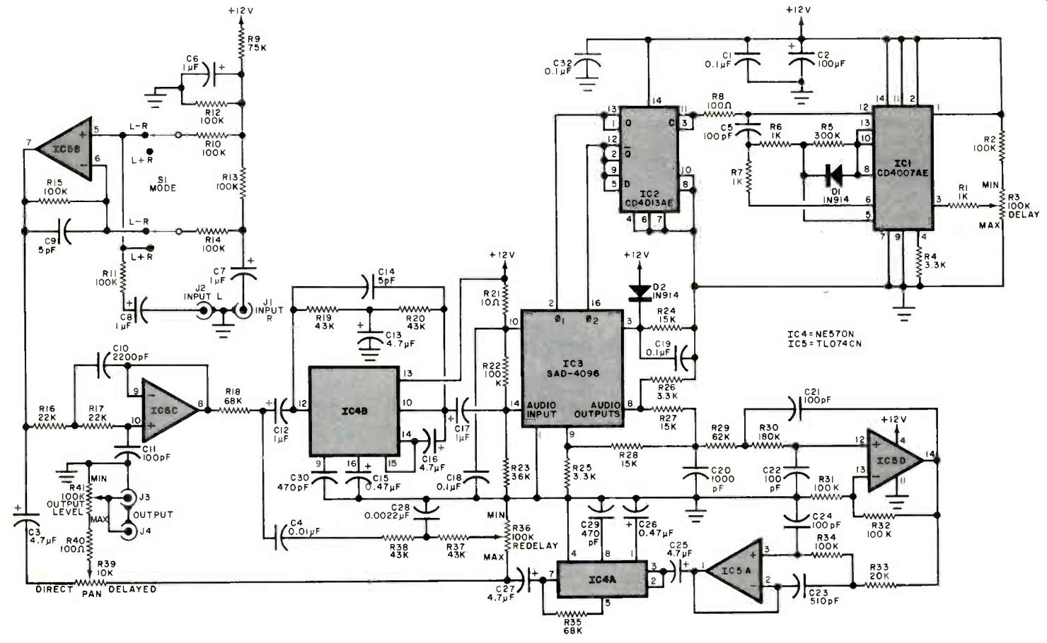
Fig. 2. Schematic diagram of the delay line. Two audio input channels
are combined by IC5C into a single channel which is delayed by IC3.
Design Considerations. A digital system's greatest advantage is that the signal degradation it introduces is fixed and independent of the length of the delay. Once a signal sample has been converted into digital form, it can be manipulated any number of times without loss. The quality of the output signal is affected only by the linearity and dynamic range of the A/D and D/A converters at the input and output.
The dynamic range of a digital system in which the digital words directly describe the corresponding input samples is approximately 6 dB per bit. A 16-bit linear digital system thus offers a dynamic range of approximately 96 dB, but is horrendously expensive. To obtain an acceptable dynamic range using fewer bits, various "nonlinear" coding schemes have been developed.
Analog delay systems bypass the complexities of A/D and D/A conversion but degrade signals more as delays become longer. Because analog shift registers are more-specialized, lower-volume devices than their digital counterparts, analog registers are considerably more expensive. In the author's opinion, analog systems offer superior price/performance ratios for delays of less than 100 milliseconds. For longer delays, he would give digital systems the nod. As 100 ms was considered a suitable upper limit for delay time in the system, the analog approach was used.
The length of delay required depends on the reverberation times that the designer is attempting to synthesize. In the author's opinion, audibly believable reverberation can be generated by feeding the output signal of the delay device back to the input.
The resulting multiple repetitions simulate the arrivals of reflected sounds along paths of different lengths. In such a system, the reverberation time can be calculated from the length of the delay and the gain of the feedback loop. For example, if the signal is delayed 50 ms and the gain of the loop is -3 dB, it will take 20 recirculation of the signal before the output level decays to 60 dB relative to its initial amplitude.
The reverberation time is thus one second.
Natural-sounding reverberation can be achieved with a maximum shift-register delay of 40 to 60 ms as long as the recirculation loop gain is well below 0 dB. A loop gain of more than 0 dB will make the system unstable.
The bandwidth of the delay line and the rate at which its input signal is sampled are intimately related. Although standard high-fidelity practice would dictate a flat frequency response between 20 and 20,000 Hz, a narrower bandwidth is appropriate for a delay line. The principal reason for this is that natural reverberation generally causes high-frequency attenuation.
Sampling theory indicates that a signal must be sampled at least twice every period if it is to be reconstructed into continuous form without error. The sampling frequency thus should be at least twice that of the highest frequency in the signal. Furthermore, a rolloff caused by the reconstruction process itself results in a response 3 dB down at approximately one-third of the sampling frequency. (This rolloff is in addition to any due to a smoothing filter at the output.) Any signal frequency greater than one half of the sampling frequency will stimulate the production of aliases or beat tones that fold back into the useful passband.
For example, if a 22-kHz signal is sampled at a rate of only 40 kHz, an alias will appear at 18 kHz. Accordingly, for all of the above reasons, it is good design practice to band-limit the signal to be sampled to about one-third of the sampling rate.
About the Circuit. The Analog Audio Delay line appears in block-diagram form in Fig. 1 and schematically in Fig. 2. The block diagram shows the principal function stages of the project.
A voltage-controlled oscillator generates a train of pulses at a rate determined by the setting of the DELAY potentiometer.
The oscillator drives a flip-flop which provides a two-phase clock signal by means of its complementary (Q and Q) outputs.
This two-phase clock governs the transfer of signal samples within the analog shift register.
An op-amp input stage accepts signals from the two main stereo channels and generates either an L+R or L-R output, depending on the position of the MODE switch. A considerable saving in system cost and circuit complexity can be realized by combining the main stereo channels to form one channel of delayed information.
Summing the two main channels before delaying them results in a conventional monaural signal that is then delayed, amplified and reproduced by a single loudspeaker. The usefulness of the L-R mode can be dramatically demonstrated by listening to a stereo FM broadcast. During the musical portion of the broadcast, relatively high levels of L+R or stereo reverberation can be introduced to provide a pleasing audio effect. When the announcer's voice is heard, it sounds as if he is talking from the bottom of a well. This can also happen when a centered vocal or instrumental soloist predominates.
The L-R mode, in which the direct center components are cancelled out, can prevent this from happening. An additional benefit provided by the L-R mode is realized because of the common mixdown practice of placing room or ambience microphones and studio reverberation unit output signals away from center. Although it is not possible to completely characterize the differences in sound quality provided by the two modes, the author's experience is that LR reverberation sounds "softer" or more subtle. The type of music and the particular mix-down will determine which mode is more pleasing.
The signal from the input network is applied to a second-order active low-pass filter with a cut-off frequency of 15 kHz.
This prevents foldback/aliasing problems that might otherwise occur. A 2:1 IC compressor acts on the filter output before it is applied to the analog shift register. Also applied to the compressor input is a signal component that is provided by the recirculation loop.
Delayed audio signals appearing at the output of the analog shift register are treated by a fifth-order active low-pass filter before being processed by a 1:2 IC expander. This filter smooths out the signal provided by the delay line and suppresses any ultrasonic clock energy contained in it.
One portion of the expander output makes its way back to the compressor input by means of a recirculation loop. This loop comprises R36, the REDELAY potentiometer, which permits adjustment of the amount of delayed signal fed back to the input compander, as well as a passive bandpass filter (R37, R38, C4 and C28). The bandpass filter provides additional high-frequency rolloff for each recirculation of the signal and some low-frequency rolloff. The accelerated absorption of high-frequency components simulates the treble loss of natural reverberation; the low-frequency attenuation prevents the reverberant signal from sounding muddy.
Complementary compression and expansion make it possible for the delay line project to have an impressive dynamic range. The rated S/N of the SAD-4096 analog shift register varies from more than 75 dB for its shortest delays to approximately 65 dB for its longest delay time.
The compansion employed in this project allows the delay system to have a very large dynamic range. As measured by the author, the IHF "A" weighted noise at the project's delayed output is-91.5 dBm at 5 milliseconds and-89 dBm at 100 milliseconds. Input-level adjustments are therefore unnecessary.
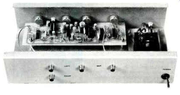
----- This photograph of prototype shows how author housed
main pc board and ac supply inside custom enclosure.
Output signals are presented to PAN control R39. This potentiometer allows the user to drive the subsequent stages in the signal chain with a fully un-delayed audio signal (when the wiper is set to the DIRECT extreme of its travel), a fully delayed signal (when the wiper is set to the DELAYED extreme of its travel), or with a mixture of the direct and delayed versions of the input signal (when the wiper is set between the two extremes of its travel). Potentiometer R41 can be adjusted for the desired balance of front to back sound levels.
Power Supply. The analog delay line project requires modest electrical power.
Its basic requirement can be obtained from any single-ended supply capable of delivering 12 volts at 20 mA. This modest amount of power can be provided from the ac power line with the ac power supply shown schematically in Fig. 3. This supply employs a center-tapped step-down transformer (T1), a full-wave rectifier (D1 and D2), four capacitors (C1 through C4), and a 12-volt regulator integrated circuit (IC1). Light-emitting diode LEDI is a convenient power-on indicator.
In mobile and many other applications, however, a source of 117-volt sinusoidal ac power is not readily available. In such situations, the project can be powered by the dc power supply shown schematically in Fig. 4. This power supply employs a zener diode (D3) as a voltage reference for an LM301 operational-amplifier integrated circuit (IC1), which, in turn, governs the operation of a pass transistor (Q1). This pass transistor acts as the regulated source for the delay circuit. The dc supply can be used with virtually any unregulated source capable of delivering + 12 to +30 volts dc. Again, LED1 serves as a convenient power-on indicator.
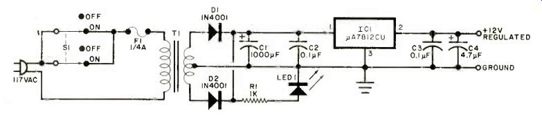
Fig. 3. This full-wave line-powered supply furnishes regulated +12
volts for the audio delay circuit.
-------------
PARTS LIST---AC POWER SUPPLY
C1-1000-µF, 25-V radial-lead electrolytic
C2,C3-0.1-µF, 50-V disc ceramic capacitor
C4-4.7-µF, 16-volt radial-lead electrolytic
D1, D2--1N4001 rectifier diode
F1-1/4-ampere fast-blow fuse
IC1--µA7812UC 12-volt regulator
LED1-Light-emitting diode
R1--1000-ohm, 1/4-watt, 5% fixed carbon composition resistor
S1--Dpdt pc-mount push-on/push-off switch or spst toggle switch
T1--20-volt, 250-mA center-tapped stepdown transformer (Signal Transformer Co. No. ST-4-20 or equivalent)
Misc.-Printed circuit board; fuse clips; line cord; strain relief; circuit board standoffs; machine hardware; hookup wire; solder; etc.
--------------
PARTS LIST--DC POWER SUPPLY
C1, C5--0.1-µF, 50-V ceramic disc capacitor
C2-100-µF, 16-V radial-lead electrolytic
C3--4.7-µF, 16-V radial-lead electrolytic
C4-100-pF, 50-V ceramic disc capacitor
D1, D2--1N914 diode
D3--6.2-volt, 1-watt zener diode (1N4735 or equivalent)
F1--1/4-ampere fast-blow fuse
IC1-LM301AN operational amplifier
LED1-Light-emitting diode
Q1--2N3906 pnp silicon transistor
The following are 1/4-watt, 5%, fixed carbon-composition resistors:
R1,R7-510 ohms
R2, R5-30,000 ohms
R3, R4-10 ohms
R6--33,000 ohms
R8--1500 ohms
S1--Dpdt pc-mount push-on/push-off switch or spst toggle switch
Misc.--Printed circuit board; fuse clips; strain relief; circuit board standoffs; hookup wire; solder; hardware; etc.
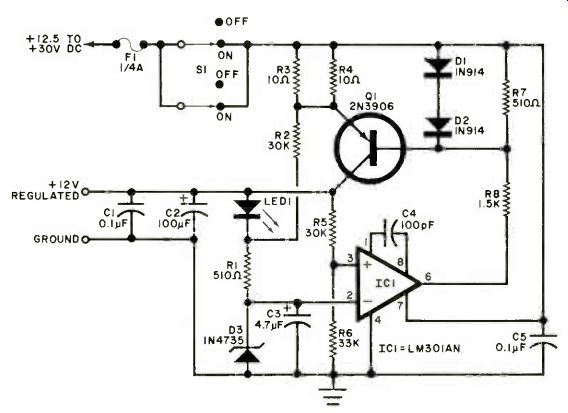
Fig. 4. This supply should be used for remote or mobile applications
when ac line power is not available.
-------------

Fig. 6. Etching and drilling guide for the ac power supply printed-circuit
board.
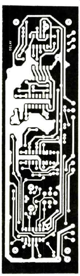
Fig. 5. Full-size etching and drilling guide for the main printed
circuit board.
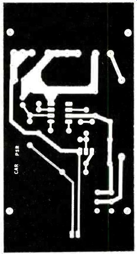
Fig. 7. Etching and drilling guide for the dc power supply printed-circuit
board.
Construction. The use of printed-circuit construction techniques is strongly recommended. Full-size etching and drilling guides of suitable pc boards for the main delay circuit, the ac power supply, and the dc supply appear in Figs. 5, 6, and 7, respectively. Component-placement guides for these boards appear in Figs. 8, 9, and 10. The main circuit board has been laid out to keep power and ground bus runs as short and direct as possible, and to prevent objectionable leakage of ultrasonic clock energy into the audio-frequency signal path.
Sockets or Molex Soldercons should be used when mounting ICs on the main circuit board, especially for IC3-any device costing that much deserves special handling. When mounting semiconductors and electrolytic capacitors, be sure to observe polarity and pin basing. Use the minimum amount of heat and solder consistent with the formation of good solder joints. Those components mounted off the board can be connected to it by means of suitable lengths of stranded, insulated hookup wire.
When assembly of the circuit boards is complete, carefully inspect them for cold solder joints, solder bridges between adjacent foils, reversed polarities, etc. Then interconnect the retain board with the power supply board that has been assembled, using short lengths of stranded, insulated hookup wire. Finally, mount the boards in a suitable enclosure, with spacers to insulate the boards from the metallic surfaces of the cabinet.
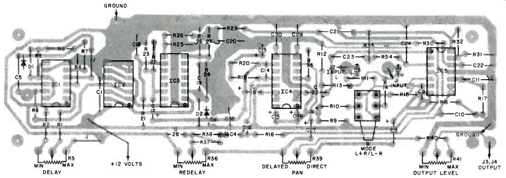
Fig. 8. Component-placement guide for the audio delay line's main
pc board.
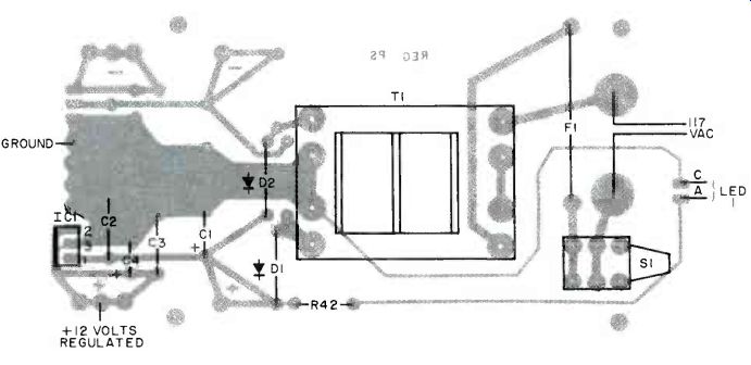
Fig. 9. Component-placement guide for the ac power supply of the project.
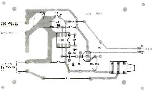
Fig. 10. Component-placement guide for the regulated dc-powered supply
for the audio delay line.
Adding It to Your System. Use shielded audio patch cords of appropriate lengths to interconnect the project with your existing audio system. The main stereo channels should be tapped at some point at which the signals are at line level. If the signals are tapped at the output of the preamplifier, the project's output level potentiometer can be used as a front-to-back balance control. If the signals are tapped before the preamplifier's volume control, the project's output level potentiometer will have to be readjusted every time the level of the front channels is changed.
A single channel of delayed audio information calls for a monophonic power amplifier and one speaker system. However, the author's prototype includes two output jacks wired in parallel so that both channels of a stereo amplifier can be driven by the same signal if desired. The rear-channel amplifier can have a power rating as low as one-fourth that of the front-channel amplifier. Excellent performance has been obtained with as little as 20 watts of rated amplifier power for the rear channel.
Similarly, the speaker system associated with the rear channel need not be as sophisticated as those used in the main (front) stereo channels. Deep bass response and extended high end are simply not needed. A speaker system with clean midrange response and a power-handling capacity compatible with the rear-channel amplifier output power will suffice.
There are no "correct" delay-unit control settings. These adjustments should be guided by the type of music being reproduced and the personal taste of the listener. Also, the amount of reverberation that will have to be introduced to achieve a desired effect will depend on the individual recording of a given piece of music.
Two discrete delay channels can share a common enclosure and power supply.
Such a configuration is available in kit form and can be connected to the main stereo channels in such a way that monaural addition or subtraction will not take place.
If desired, one clock can be used to drive both stereo delay lines so that the delay times track each other. A richer sound may result if each channel has an independent, adjustable clock.
----------
KIT AND PARTS AVAILABILITY
The following are available from Phoenix Systems, 91 Elm St., Manchester, CT 06040: Complete kit of parts, including enclosure, for a single-channel, dc-powered delay line, No. P-25-DLC, for $145; complete kit of parts, including enclosure, for a single-channel ac-powered delay line, No. P-25-DL, for $150; complete kit of parts for two-channel ac-or dc-powered (specify) delay line, No. P-25-SDL, for $250. The following are also available separately from the same source: SAD-4098 bucket-brigade analog shift register IC, No. P-SAD-4096 for $40.00; etched and drilled main printed-circuit board, No. P-25-DB, for $8.00; NE570N compander IC, No. PNE570N, for $4.50; Signal Transformer Co. No. ST-4-20 step-down transformer, P-94-T, for $6.50; etched and drilled ac power-supply printed-circuit board, No. P-25-PSB, for $5.00; dc power-supply board, No. P-25-PSBC, for $5.00; TL074CN high-performance quad bi-FET operational amplifier, No. PTL047CN, for $2.50; µA7812UC 12-volt regulator IC, No. P-7812UC, for $1.50; 100,000-ohm linear-taper, pc-mount potentiometer, No. P100KB, for $1.00; 10,000-ohm, linear-taper, pc-mount potentiometer, No. P-10KB, for $1.00; push-on/ push-off pc-mount dpdt switch, No. P-2PDT, for $1.00. Add $1.00 handling charge for orders less than $10. All items postpaid within continental U.S. COD orders subject to $2.00 surcharge. Connecticut residents, add state sales tax.
--- External (above) and internal (top) views of author's
prototype.
In Conclusion. Psychoacoustics is still as much an art as a science and remains a fertile field for experimentation. The analog delay line that has been presented here is designed with the adventurous, inquisitive audiophile in mind. It is, therefore, well suited for those readers who want to experiment with time-delay techniques.
Source: Computers and Electronics--Experimenter's Handbook (1984)
Also see: Do-It-Yourself Logic Chips
Cancel Rumble With This Bass-Summing Amplifier