AMAZON multi-meters discounts AMAZON oscilloscope discounts
IC and System-Level ESD Stress
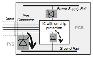
Fgr. 1 ESD current path in a system with internal IC.
An ESD event represents the transfer of energy between two connected objects with different electrostatic potentials until the potentials become equal or the connection is removed. The ''connection'' assumes the current path provided by any media including air. An ESD event results in a decaying current pulse proportional to the level of the electrostatic potential difference and the rise time and current level determined by the impedance of the connection. The transfer occurs either through contact or via an ionized ambient discharge (a spark). This transfer is modeled in various standard circuit models for testing the compliance of device to corresponding passing level. Typically, these models use a capacitor charged to a given ESD pulse voltage and a network which acts as a current-limiting resistor (or ambient air condition) accompanied by inductive and capacitive loads to control the pulse rise time and waveform parameters. The specifications of the ESD pulses, standards and test methods are summarized in Sect. 2.
ESD transient current pulses have ~1-200 ns duration with the rise times from a few hundreds picoseconds to a few tenths of nanoseconds and current amplitudes from ~1 to over 50 A. Unless special protection measures are taken, at certain critical amplitude the ESD transient current pulses may directly impact the reliability of both the systems and components. This can result in a reduction of the manufacturing yield or loss of consumer products.
In real life, ESD discharges can strike the system or devices during their product lifetime by the end user, during manufacturing and assembly or maintenance, as a result of a discharge after triboelectric charging, interfacing with other charged systems or devices in form of mechanical connection of the conducting surfaces or by air discharge. For example connecting charged cables or connectors to a system input and output port can create a discharge current that must be dissipated inside a system through a dedicated ESD current path ( Fgr. 1, above).
The clamping voltage and residual current realized in an IC are functions of the breakdown voltage and the dynamic resistance of the protection device. The clamping voltage can be extrapolated by multiplying the current on dynamic on resistance of the circuit involved in the ESD current path.
To guarantee the reliability and certify of the systems both the component and system-level ESD qualification tests are carried out based on a set of corresponding standardization documents. This qualification tests conduction is an undividable part of both the IC and system design and production. Passing these tests is a requirement to obtain different product certifications, for example the CE mark in Europe, necessary for the introduction of products in the consumer market.
Meantime the ESD protection strategy itself is based on a rather simple approach. It consists of an implementation of a dedicated current path for the discharge by means of either on-chip protection structures in case of IC components or/and embedded into a system ESD protection network. The network protects the system itself in addition to other isolation measures. This protection network is usually composed using active and passive on-chip and off-chip on board components. Altogether the components and interconnects essentially rep resent a pulsed power network circuit that remains passive during normal operation, but becomes active during ESD pulse providing the discharge current path.
The ESD pulse protection network activation is typically realized by a combination of the rise time and overvoltage detection. In this case on-chip and off-chip ESD protection network components turn on if a critical voltage at the IC pins or system ports exceeds a certain threshold value.
Trends in the IC Component and System ESD Design
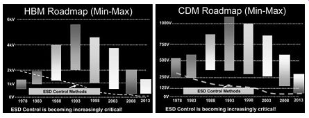
Fgr. 2 ESD pulse roadmap suggested by the EOS/ESD Association for HBM and
CDM stress.
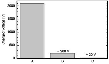
Fgr. 3 Impact of different ESD control methods on the voltage of a person
in a manufacturing environment: a. no ESD control; b. ESD flooring installed;
and, c. ESD flooring installed and ESD footwear used data from [2].
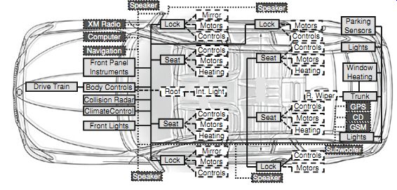
Fgr. 4 Illustration of the robust system-level design approach for automotive
products.
The level of ESD that an end-user can generate and introduce into an electronic system product during its lifetime is much more severe than the typical level generated in a controlled manufacturing environment. Moreover, since the introduction of the S20.20 procedure [1] in year 1993, the ESD pulse levels detected in real ESD controlled environments have a continuously reduced trend. As a result, the EOS/ESD Association (ESDA) has proposed a corresponding reduction of the qualification requirements (Fgr. 2). This initiative has not been fully accepted by the industry yet and the standard corporate requirements from IC manufacturers and particular product specifications are often dictated by customers. They typically include 2 kV HBM and 100-200 V MM ESD pulses for the component level. However, the fact of the significant reduction of the ESD stress event amplitudes in the ESD protected areas hardly causes any doubts and it’s widely used at least for the passing level waiver justification.
ESD control programs significantly reduce the accumulation of charges in a manufacturing place. For example in case ''A'' ( Fgr. 3) the voltage on the person is measured when no specific ESD control method is in place. It can reach over 2 kV. If the manufacturing place is equipped with an ESD floor the electrostatic induced voltage is reduced down to ~200 V level ("B", Fgr. 3). If the operators wear ESD footwear the walking on the ESD floor generates only ~20 V ("C", Fgr. 3). Thus the voltages generated by the person can be reduced by two orders of magnitude by implementation of the ESD control programs.
An opposite trend over recent two decades was observed for the system-level protection where a number of new standards have been introduced to support the elevated ESD protection requirements of systems. One of the typical examples is to address requirement for zero defect part per million failure rate in automotive applications ( Fgr. 4). In addition to the system level ESD pulses a number of new for IC manufacturing standards have been propagated down to the component level. This includes power surge specifications (Sect. 2). Thus a major paradigm shift had occurred when these, originally system-level standards, have been propagated down to the requirements of the passing level of selected pins of IC components.
To some extent the emphasis on ESD protection has been shifted from the chip level ESD robustness to the system robustness. In the past the original attempt to address this was made by intuitive requirements of just a higher passing level of the standard component-level ESD tests. The IC manufacturers were requested to supply IC with some pins protected up to For example 8 kV or even 15 kV HBM.
Even today such an unreasonably high (comparing to Fgr. 2) components HBM stress level can be found in datasheets of some new product listed together with the system level passing data. However, the passing level for the specific system-level standard pulses became a dominant approach.
In general the component passing level for CDM, MM and HBM standard pulses at the chip level don’t guarantee a system-level added robustness of the IC.
The discharge through the IC during chip-level ESD qualification is applied in power-off conditions. In general the resultant ESD current path is not the same during a system-level ESD test in a powered-up system. Therefore the capability of IC to withstand at least a fraction of the system-level ESD current needs to be verified. This should be done for the IC pins directly interfacing with the system ports unless a board-level ESD protection network guarantees the appropriate limitation of the current into the IC pin.
The original purpose of the chip level verification is to guarantee the reliability of the chip itself during the manufacturing processes and assembly of the system itself, rather than during the life cycle of the system in the field. A system might experience rather high failure rates in the field and unlikely will pass certification unless the system is specifically designed to dissipate any ESD discharge by an intentional implementation of a system-level ESD protection network.
The most optimal design approach today to implement ESD robust system-level design involves both the IC component and the system board protection levels.
On-chip ESD protection network is typically composed of ESD clamps, diodes, self-protected power devices and robust metal busses and interconnects to conduct the component-level ESD currents. The system-level ESD protection networks rely on passive components in addition to optional transient voltage suppressors (TVS). The major strategies to combine both networks will be reviewed in the following two sections.
There are two important trends leading to fundamental changes in ESD protection strategies at the system design level-increased susceptibility of system level ICs to ESD with migration toward more advanced process technology nodes and increasingly stringent signal integrity requirements as data rates continuously increase [3].
The traditional approach to deal with higher data rates is to reduce the capacitive load in the transmission line. This includes the capacitance of the ESD protection device. However the capacitance of the ESD device is proportional to the device active regions width. A reduction of the ESD protection capability of the device is an expected undesired side effect. As a result, system designers become under pressure to make tradeoffs between their system reliability and signal integrity or involve matching networks and ESD protection co-design strategies.
For certain signal integrity requirements the traditional system-level ESD approach cannot deliver suitable protection solutions due to the limitation in the semiconductor process technology used. Therefore an off-chip ESD protection design becomes unavoidable. In general the clamping voltages and residual current levels that were acceptable in previous generation of application specific ICs are no longer suitable for the new generation circuits implemented in the scaled semiconductor processes. Adoption of high speed data interfaces USB, HDMI and Display Ports adds to the complexity of maintaining the signal integrity under robust ESD protection. Similar trends can be observed in RF antennas, automotive networks, medical, industrial and even emerging servers for cloud computing applications.
The changes of the application environments directly contribute to the ESD vulnerability. For example various handheld and mobile devices are now being used in everyday harsh and uncontrolled environments with real life ESD events generating system-level ESD pulses up to 30 kV, power surge and EMI. The devices must regularly withstand multiple cable connections and disconnections to the system ports, accumulation by the isolated portable device triboelectric charges in different application conditions like for example in the pocket of a running or biking person.
With traditional ESD architectures, an inverse relationship between robust ESD protection and low parasitic capacitance negatively impacts the signal integrity.
This results in an increasing difficulty of maintaining capacitance and impedance matching. On the other hand, the combination of multiple specifications, standards and testing criteria are often quite cumbersome. Identifying which ESD protection approach and device provides the best results is rather difficult due to unclear voltage clamping waveform realized by the off-chip devices under system-level ESD discharge conditions and by the on-chip devices at the residual current propagated to the IC pin.
Top of page Article Index HOME