AMAZON multi-meters discounts AMAZON oscilloscope discounts
The original role of an on-chip ESD protection is to guarantee that an IC is capable of withstanding the ESD stress through its entire manufacturing process in an ESD Protected Area (EPA). This includes both chip foundry and system assembly.
Respectively the qualification of each chip includes requirements for certain passing level for the pulses defined by the various standards. The component level standards have been established to verify the immunity of the IC's in the con trolled ESD environment. The major standards include: The Charged Device Model (CDM), Machine Model (MM) and Human Body Model (HBM) ( Fgr. 5).
CDM testing verifies the susceptibility of the IC to a discharge event from the charged package to a grounded metal object. This pulse has a fast rise time ~100 ps, very short 1-5 ns, and its amplitude is proportional to the IC component size. The IC package can accumulate charges at a given electrical potential. The typical test levels for CDM are between 250 and 750 V.
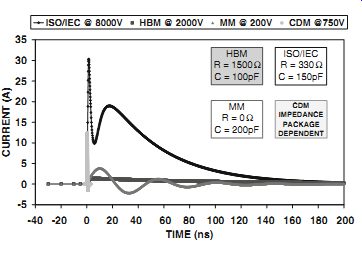
Fgr. 5 Comparison of the idealized waveforms for major IC component and IEC
system-level pulses.
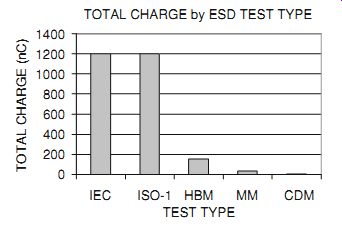
Fgr. 6 Comparison of the total charge for major IC component and IEC system
level pulses.
The MM ESD event physically represents the discharge of pre-charged metal tools that are suddenly connected to an IC pin. It’s assumed that the IC has connection to the discharge ground path. Due to inductance of the metal tool the pulse has an oscillatory waveform. It’s expected that in an EPA the metal tools unlikely can be charged up to a too large electrical potential due to their low resistance and if proper grounding procedures are in place. Therefore typical test level for MM is either 100 or 200 V. The 200 V pulse produces ~3 A peak current.
===
Table 1: Comparison of two major ESD protection strategies
Local clamp network; Rail-based network
Advantages: Independent of bus resistance; Local to every pin; Suitable for multiple pin count; Does not require pad ring SoC and system-level design.
Area efficient; Highly process portable SPICE-based design; Optimal for small pin count IC.
Drawbacks: More area intensive; Highly process sensitive; Difficult to simulate and account for ''sneak'' current path; Performance based on bus resistance; Distributed ESD network requires complex chip level implementation and verification.
===
The HBM standard physically represents the discharge of a charged person to an IC pin with another IC pin grounded. It’s agreed that the electrostatic potential generated by person within EPA is between 0.5 and 2 kV. The generated current pulse is limited by a 1.5 kX discharge resistance which results in a peak current of ~1.33 A for a stress level of 2 kV.
These IC component test voltage levels ( Fgr. 2) are only meaningful in a controlled manufacturing environment within an EPA, where precautions are taken to ensure that static electricity levels on personnel and equipment are minimized.
System-level stress pulses at the same pre-charge voltage result in significantly larger pulsed current amplitudes ( Fgr. 5) and total charges ( Fgr. 6). The sys tem-level standards are discussed in details in Sect. 2.
On-chip ESD protection network is represented by an embedded power circuits that provide different reversible current paths for each IC pin-to-pin combination.
At the discharge through these current paths an appropriate voltage limitation is realized in order to prevent any irreversible changes of the protected internal circuit. In spite of the high variety of analog circuits, the network can be constructed based on rather common simple principles. Typically networks are differentiated as the local clamp based or as the rail-based network. The first may also include self-protection capability of the on-chip active circuit components.
The local protection network relies on a dedicated ESD protection clamp attached either between the protected IC pin and IC ground or between two IC pins. In this case the current path is expected to be realized for each pin to pin combination through the local clamp. The alternative rail-based network delivers the protection of the same power domain IC pins through the diodes connected to the ESDPLUS and ESDMINUS rails with core clamp connected. The current path between two pins is realized through the diode and the core clamp network. Both approaches have advantages and drawbacks (Table 1).
Design of the ESD protection network includes an appropriate selection of ESD clamps developed for a given process as an intellectual property (IP) and compatible with the process design kit (PDK), design metallization routing adequate to conduct the large ESD currents, and accounting for the alternative current path(s) throughout the internal blocks of the analog circuitry. The choice of the local or rail-based clamps for different power domains is an application-specific task. Due to interaction of analog I/O blocks with the active internal circuitry both mixed mode simulations and circuit ESD simulations with compact modeling tools are used to provide an important design verification and optimization.
Overall on-chip ESD protection network strategies are described in details in [5]. The major function of the network is to react on high transient voltages by enabling a discharge current path. Depending on the internal circuit specifications, both transient-triggered and voltage-reference ESD clamps can be used to implement the on-chip protection network. Design of the protection clamps for the component-level specifications is broadly discussed in [5]. The specific of ESD clamp design for system-level pins is discussed in Sect. 3.
The term ESD pad ring is often used in digital circuit design or in small pin count analog circuits where the periphery of the chip is used for I/O and power supply pads, ESD clamps and I/O circuit placement. Any ESD pad ring includes pads and a distributed ESD protection circuit created near the pads from a combination of cells. ESD protection network components can be embedded in the I/O cells too. In most cases, the ESD pad ring can be decoupled from the internal circuitry and then practically reused to support different internal circuit blocks.
For analog circuits, understanding of the ESD pad ring design is not always as straightforward as for digital circuits. The complexity is the result of a greater level of interaction of the current path with the internal power circuit. Often, an analog circuit pin can interface with many connected active devices. Thus inside of the internal circuit some, especially power, components may see a significant residual ESD stress.
In the case of micro SMD or wafer level flip chip packaging design the bump pads are arranged in form of ball grid array on top of the whole silicon die area. In this flip chip package the implementation of the ESD pad ring becomes impractical.
Although ESD network generally may not be decoupled from the internal analog integrated circuit the ESD current path and voltage limitation can be still analyzed to a certain level using hierarchical and mixed-mode simulation methods.
Depending on the internal circuit design, the absolute maximum voltage of the internal components may significantly vary due to different coupling of the control electrodes of the output devices. From this prospective, power analog circuits and ESD protection networks often may require custom co-design, especially when system-level requirements are specified for certain IC pins.
Rail-Based ESD Protection Network
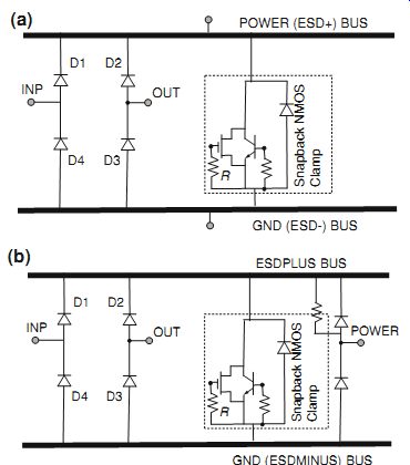
Fgr. 7 Rail-bases ESD protection network with snapback clamp as a power clamp
(a) and as a core clamp (b)
To pass the ESD qualification each IC pin must rely on either self-protected by the internal power devices or must be connected to the ESD protection network. Local ESD protection is independent of bus resistance, as well as of other network components. It provides a relatively easy accountable local voltage waveform at every pin. But it’s not an optimal space-saving solution and more process-sensitive especially in case of high voltage tolerant analog IC pins.
In general a rail-based ESD protection network can be composed of diodes and so-called core clamps connected between ESD rails. In principle ESD rails can share the power supply busses or be independent from them. The core clamps can have either snapback or non-snapback characteristics. However when snapback clamps are used the total accumulated voltage drop might become excessive to limit the voltage at the pin at the appropriate level. Therefore the approach has a limited use, for example for amplifiers with large ESD protection windows.
Rail-based protection can be implemented with the core clamp acting either as a power and core clamp or just as a core clamp. In the first case the ESDPLUS and ESDMINUS rails are the same as ground and power supply, for example VDD and VSS ( Fgr. 7a). For the core clamp functionality the power supply can be connected similarly to the I/O through the rail diode pair ( Fgr. 7b). In this case, if an active clamp is used, a charge ''bleeding'' resistor must be used from the ESD PLUS rail to any other pad in order to avoid the internal charge accumulation and corresponding disabling of the active clamp as a result of multiple ESD pulses.
A rail-based ESD network can be identified by the presence of ESD busses (rails) with the shared core clamp and the ESD diodes connecting the other pins to the rails unless the diode function is accomplished by the body diodes of the appropriately large internal devices connected to the pin. ESD diodes can connect input/output (I/O) pins or other control pins, including power supply pins. The power supply pins connected to the rails typically share the metallization routing.
However, in principle, the network can be organized with ESDPLUS and ESD MINUS busses that separate the power supply and ground for the domain.
ESD protection can be embedded in the input/output (I/O) cells. Under this approach, a set of ESD and latch-up rules must be taken into account to provide a non-conflicting operation of ESD elements and I/O cell components. The latch-up physics and related design aspects are discussed in Sect. 4.
One of the major advantages of the active clamp network design is a direct applicability of circuit analysis for ESD pulse operation with regular active device compact models. In the case of the rail-based network, there are several steps in the complex chip verification. They usually include: verification that every IC pin has ESD protection; analysis of the dedicated ESD discharge paths and pin-to-pin voltage drop; extraction and verification of interconnect robustness for the ESD current density level (in contacts, metal and vias); verification of ESD cells types, their dc voltage and pin signal tolerance as well as compliance with ESD design guidelines.
In rail-based ESD protection, the ESD diodes are expected to conduct pulsed ESD current only in the forward bias mode and have high reverse breakdown voltage protected by the ESD network. To avoid interference with the major ESD current path, the voltage tolerance of the ESD diodes is an important parameter.
An appropriate breakdown voltage of the rail-based protected domain-above the power supply level-should be provided to avoid ESD diode burnout due to avalanche breakdown mode and to minimize direct impact on circuit functionality during normal operation.
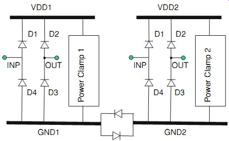
An example of the simplified 4-pin rail-based circuit ( Fgr. 7a) combines the protection of the input (INP), output (OUT), POWER, and ground (GND) pins.
Additional pins can be added to the network by reusing similar diode connections to the I/O pins. For each pin-to-pin combination the network delivers an ESD current path through the forward-biased ESD diodes, corresponding parts of the rails and the core power clamp. Both the high-voltage current path and the reverse path through the clamp diode are realized in the power clamp. For example, at positive ESD zap of INP versus OUT, the current path is formed through the upper diode D1, the upper part of ESDPLUS bus, then through the snapback clamp, the corresponding part of the ESDMINUS bus, and the forward-bias diode D4.
Rail resistance should also be taken into account at ESD current level, the total voltage drop on the circuit and the voltage drop at each pin relative to the ground can be estimated for the clamp voltage drop VC, forward-biased diodes voltage drop VD and the contribution of bus resistances RESD+ and RESD- depending on the current path (Table 1.2). Certainly more complex multiple pin count cases require CAD automation tools for the automatic extraction of multiple current path resistances [6].
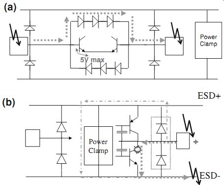
In the distributed network the clamp components can be shared. For example the distributed core active clamp includes multiple instances of NMOS arrays with shared RC-timer ( Fgr. 8). The advantageous low on-state resistance of the distributed network of RC-controlled power NMOS devices delivers rather low clamping voltages across the pad ring area that is proportional to the number of distributed cells used.
If the system-level requirements are important the chip-level protection with active clamps becomes rather challenging since active clamps are disabled when the power supply voltage is present. To limit the voltage at the input pins, anti parallel diode clamps with a number of diodes that corresponds to the desired differential signal level are used to protect the differential BJT input pins ( Fgr. 9).
===
Table 2 Rail-based peak voltage at peak ESD current ESD zap combination Total voltage drop on zap pins INP voltage versus ESD- OUT voltage versus ESD+ POWER voltage versus ESD INP to ESD+ VD VD 00 PWR to ESD- VD ~VD/2 ~VD/2 VD ESD- to INP VD VD 00 PWR to ESD- VC VC/2 VC/2 VC INP to OUT 2VD+ IH(RE- + RE+) ? VC VD+ IH(RE-+ RE+) ? VC VD ~VD INP to ESD- VD+ IH(RE-? RE+) ? VC VD+ IH(RE-+ RE+) ? VC (IH(RE-+ RE+) ? VC)/2 IH(RE-+ RE+) ? VC
===
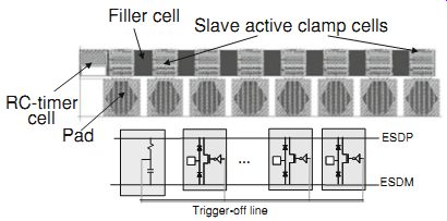
Fgr. 8 Example of layout and schematic views for 3 V ESD domain active clamp
network composed from ESD library cells
Fgr. 9 Example of rail based bipolar differential input (a) and output protection
(b) with indicated ESD current path
Local Clamp Network and Two Stage Protection
Fgr. 10 Example of a 4-pin local clamp based protection network
Fgr. 11 Two-stage ESD protection for CMOS input (a), the local based network
with the second stage avalanche diode (b) and ESD protection for a high-speed
receiver with a two-stage matching resistor (c)
Fgr. 12 Simplified circuit diagram of an NMOS output pad with a current-limiting
transistor and an additional local clamp for ESD protection.
The rail-based network for IC inputs and outputs is usually inefficient in case of system-level ESD stress due to the high voltage drop accumulated by the network.
Under power-on conditions the active clamp is disabled and thus may not sufficiently react on the ESD pulse. Other cases preventing the active clamp approach involve the protection of the pads with a voltage tolerance above the rating of the available active devices, for example in the case of amplifiers realized in a 5 V semiconductor process with high common mode 65 V tolerant differential input pins connected to thin film input resistors [7]. Additional examples include circuit pins with dual-direction high voltage tolerance. Protection solutions for such pins may not tolerate the lower diode-to-ground rail and thus require also an exclusion of the upper diode-to-power-supply rail. Therefore the local clamp approach represents the only practical solution ( Fgr. 10). In the local ESD protection network approach every pin is protected by a dedicated local ESD clamp that delivers a current path either from pin to the ground or directly another pin.
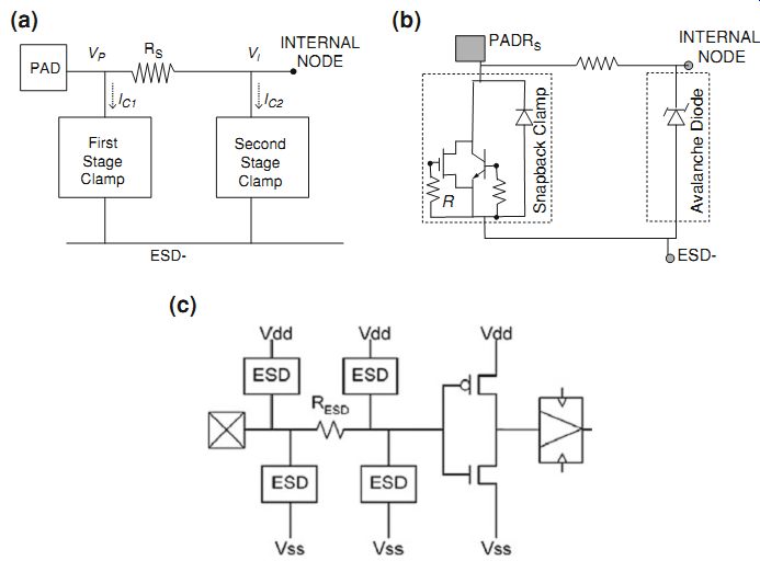
A two-stage on-chip ESD protection principle is applicable for local clamp protection. In general the two-stage network consists of a combination of two ESD clamps separated by a resistive current path or a delay component. The resistor based two-stage network ( Fgr. 11a) combines the primary clamp that limits the operational voltage to VP, while the smaller secondary clamp limits the voltage at the internal node to VI. The second stage resistor RS is selected depending on the second stage clamp current IC2: RS = (VP- VI)/IC2. The two stage clamp is very efficient in filtering the short pulse overstress which is typical for CDM events due to the RSCI time constant. CI is the equivalent capacitance of the internal node. The use of secondary clamp becomes optional if the internal device can support an adequate pulsed current level.
The two-stage protection against system-level ESD pulses is similarly applied both on-chip and on board. On PCB the advantage lies in the high capacitance and inductances of discrete components, while transient voltage suppressor may function as a primary protection stage.
An example of the two stage network is a first stage snapback clamp separated by a resistor from a second stage and a voltage limiting avalanche diode ( Fgr. 11b) or two stage diodes with a matching resistor ( Fgr. 11c). The primary clamp directly interfaces with the input PAD. It limits the voltage only to certain extent and conducts the most of the ESD current. However the primary camp can be designed to target the clamping voltage waveform only approximately. This separated function is addressed by a more precise, but less robust secondary clamp.
The result of the separation of the current and voltage limiting function between the local protection stages is an overall decrease of parasitic capacitance, leakage and noise.
An additional advantage can be taken from implementation of non-linear resistors used in the stage. For example it can be implemented as a saturation resistor (RS Fgr. 11a) that provides an additional voltage drop starting from some saturation current level.
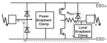
The principle of the two-stage network is widely used across both the component and the system levels protection for inputs and outputs. In case of outputs the internal circuit power arrays may provide an appropriate matching current for the second stage protection even in cases where the stage separation is only accomplished with metallization resistors ( Fgr. 12). The complexity of local ESD protection is related to generally unknown conditions of the control electrodes of the devices interfacing with the pad during ESD pulse. As a result the triggering voltage of the internal devices can become comparable to the triggering voltage characteristics of the ESD clamp.
Under power-on system-level test conditions the local snapback clamp needs to be chosen by taking into account the potential transient latch-up issue. For example various silicon controlled rectifier (SCR) devices (Sect. 3) generally produce a relatively low holding voltage below the power supply level and thus provide a latch-up risk.
The two-stage principle can be implemented also at the device level. An example of a compact solution is represented by a three-terminal diode structure ( Fgr. 13a, b). It incorporates two-sided diodes that form a three-terminal structure. One side of the diode is used for power ESD operation (a power diode connected to the I/O pad) and the other side just holds the lower potential in the internal circuitry (a potential diode connected to the internal circuitry). Both internal diodes share the same well, thus creating a two-stage ESD protection circuit with a corresponding ''built-in'' internal well-resistor. An important feature of the diode structure is the internal potential sharing during ESD operation.
The ESD protection of the I/O pin can be realized using a corresponding circuit presented in Fgr. 13c. Operation of the two-stage components can be analyzed using numerical simulations of the device cross-sections ( Fgr. 13d) demonstrating over two time's lower voltage at the internal node.
The two stage approach can be effectively used to resolve the issues in the entire ESD pulse time domain. For example it can be used to limit the residual voltage at the internal after the snapback device triggering off. This can be illustrated by an ''Erase'' pin protection case in an EEPROM memory module with external programming.
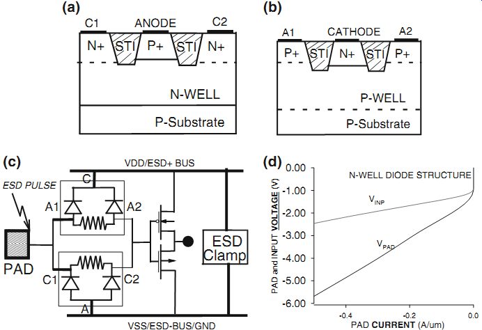
Fgr. 13 Three-terminal diode structures for nWell (a) and pWell (b) diodes
with device level 2-stage protection principle implementation, corresponding
rail-based network (c) and calculated voltage drop the pad at the internal
node for the nWell diode as a function of the pad current (d).
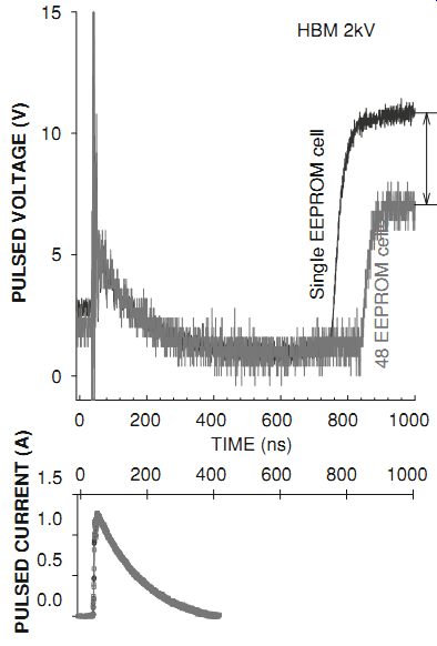
Fgr. 14 Voltage and current waveform for the EEPROM with single cell and
48 cell arrays measured at 2 kV HBM.
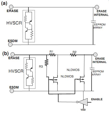
Fgr. 15 Original (a) and modified (b) EEPROM Erase pin protection clamp circuit
to reduce the residual voltage after SCR turn-off.
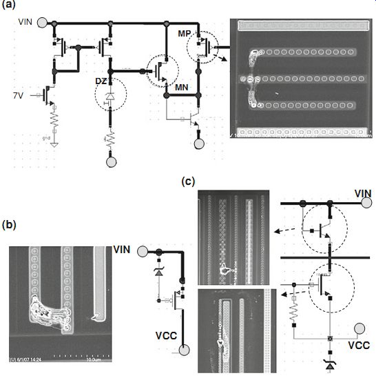
Fgr. 16 Examples of the FA results for PMOS (a, b) and NPN BJT based VCC
regulators (c) [5]
The failure was observed in form of a reprogramming of the memory cells as a result of ESD stress due to combination of the high residual voltages at the erase pin with other nodes potential at the remaining ESD stress steps after ~800 ns from the beginning of the pulse. The measured waveform at the original SCR based erase pin protection delivered different load dependent residual voltages ( Fgr. 14). With the small load with only one EEPROM cell the reprogramming as a result of ESD stress was observed in comparison to the case of higher load with 48 EEPROM cells.
To reduce the residual voltage the original HV SCR based circuit ( Fgr. 15a) has been modified with a second stage component and additional feedback loop ( Fgr. 15b). An enable module has been added to disable the second stage clamping during normal operation.
The local on-chip protection is not only limited by the local clamping of the peripheral pins. In addition to the goal of achieving a good ESD performance the local clamps can be included in the internal circuit. One of the most typical examples of the impact of ESD stress on the internal pins in high voltage circuits is the internal voltage regulator of low side control circuits, logic and drivers for switching devices. Because of the relatively low impedance of internal regulators, a second stage resistor often cannot be used in order to realize the two-stage protection approach. As a result, the regulators can exhibit increased sensitivity to ESD damage and therefore must be designed to withstand certain ESD current levels. Usually, the internally generated VDD voltage node requires an internal voltage clamp capable of handling high ESD current. Such a clamp is applied even if the VDD node is not connected to the external pin at all.
The most typical locations of failure in internal voltage regulator designs are the high-side high-power components. In the high-side PMOS-based regulator the high-voltage PMOS fails ( Fgr. 16a). In this case, the gate clamping diode may not provide a substantial improvement ( Fgr. 16b). A similar ESD current failure path was observed in bipolar and stacked regulators. In this case, due to the domino effect, damage in both stacked components might be observed ( Fgr. 16c). ESD protection of the high-voltage PMOS used in VCC regulators ( Fgr. 16) is based upon the expected ESD path formation between the VIN and CBOOT pins.
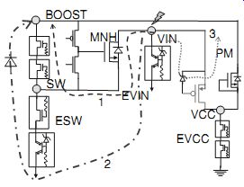
Fgr. 17 Simplified circuit of the DC-DC voltage regulators with three possible
ESD current path scenarios for VIN to CBOOT ESD zap
In general, there are three current paths that could be realized for ESD pulse current ( Fgr. 17). The first current path is provided by the large switching NLDMOS controlled by the driver. The NLDMOS turns on for a short period of time due to the drain-gate coupling that may be sufficient enough to discharge the ESD current. This current is directed to the switch pin SW, followed by the reverse current path through the BOOST-SW clamps. The clamp's reverse path ESD diode provides this remaining current path. This current path is reversible in properly designed ESD protection clamps. The second alternative current path is realized through the high-voltage ESD clamp to the power ground, followed by the ESD diode between the BOOST and ground. This current path is also reversible.
Finally, the third, and generally irreversible, current path is provided by the high-voltage PMOS and other stacked components of the regulator ( For example, the NPN diode shown in Fgr. 17) directly to BOOST pin. If this current path is dominant, the PMOS is exposed to failure. This current path explains the scenario demonstrated by Fgr. 16a, b.
At low level of array coupling and a small ESD protection window, ESD failures are related to the internal voltage regulators and they require product specific measures to overcome the triggering voltage variation in the HV ESD protection VIN clamp, dependence of the NLDMOS array self-protection capabilities upon layout and internal circuit driver design, variation of the pulsed SOA of high-voltage PMOS and NLDMOS devices.
The specific way to improve ESD protection depends on the dominant ESD current path realized in the particular product circuit. Perhaps, the first, most logical solution is to improve ESD protection by reducing the VIN clamping voltage to a lower level, thus limiting the voltage drop on the PMOS device.
However, this adjustment of the parameters of the high-voltage ESD protection clamp might not be an option in case of relatively low safe-operating area (SOA) margins of the power-optimized components. In this case, the most robust way is to implement ESD oriented co-design of the VCC regulator, which provides a much higher pulsed absolute maximum voltage for the circuit pins. Design measures may include stacked or oversized components or application of less power efficient components with higher voltage tolerance, if allowed by the process. To protect the low side driver an additional internal power clamp may be required.
Multiple Voltage Domains
When the analog circuit has different voltage domains, the ESD protection net work can be constructed using several approaches that depend on circuit specifications. The most typical example of a multiple voltage domain circuit is in the combination of the digital, analog, and power domains. Since the ESD protection of a chip is required to withstand each pin-to-pin combination, all domains should be connected into a network.
Consider an example of analog and power domains. The inter-domain connection in the network is usually realized between the power and analog grounds.
The simple reason for this arrangement is that the power supply voltages cannot be shared. To avoid cross-talk due to the potential drop on the ground busses, the grounds can be connected using a back-to-back diode clamp. This clamp decouples the ground bus interference on the voltage drop on the forward-bias diodes and, at the same time, will provide a low voltage drop at ESD current level ( Fgr. 18). In this case, the stress on the pins from the different domains will include the additional voltage drop on the diode. A similar approach is used in the case of a two-voltage domain with a distributed active clamp network.
The case of back-drive compatible pins is one of the examples of when a rail based ESD protection network with diode clamps is not possible. The pin must be independent from power and thus the diode-to-ESD+ rail is not suitable.
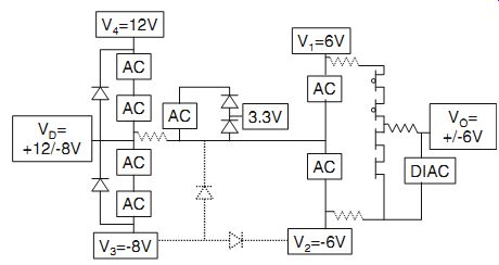
An example of multiple voltage domains with level shifts used in LCD display applications is presented in Fgr. 19. This application is designed to operate at a substrate voltage of -8 V with power supply pins of -8, -6, 0, 6, and 12 V.
The analog circuit is completed using 3.3 and 6 V isolated CMOS devices. The ESD protection network combines five blocks with separate ESD clamps: distributed active clamp (AC) blocks, with a clamp width of W ~500 lm, Lg = 0.8 lm, and an RC timer with RC = 4 uS; 6 V NMOS snapback clamp; dual-direction ESD devices for 3.6 V inputs and dual-direction ESD devices for 20 V inputs (level shifter).
The ±6 V-tolerant input pin VO is protected by the dual-direction DIAC ESD clamp ( Fgr. 19) or by the substrate-isolated stacked back-to-back snapback NMOS clamp. The parasitic resistance and parasitic diodes in the internal circuit ( Fgr. 19, dotted lines) can provide the additional voltage drop and the alternative current path, respectively. These parasitic components of the network should be accounted for.
Fgr. 18 ESD protection network for multiple voltage domains with the antiparallel
diode clamp
Fgr. 19 ESD protection network for LCD driver using DIAC protection for output.