AMAZON multi-meters discounts AMAZON oscilloscope discounts
This section presents the key simulation-based methodology for industrial on-chip and off-chip system level ESD design. The examples of this methodology application are widely presented across the guide sections.
Industrial ESD Development Workflow with TCAD
Industrial ESD IP development for a new mixed-signal process technology is usually initiated simultaneously with the process specification definition. Typically, several learning cycles toward the physical development of ESD devices and clamps are required and combined with an extensive test chip experimentation to target the desired parameters. When all the development objective choices are finalized, the ESD design and collateral are released together with the process development kit. The ESD IP typically combines layout, schematic and symbol views supported by the ESD library datasheet and design guidelines. In addition latch-up, IC-level ESD scheme and layout verification decks are often provided. At the process development and qualification states design and verification of the lead analog products are conducted. After this development period a number of custom ESD solutions are often added across the entire life span of the process technology, which targets additional optimization and specific product cases.
With each next step of this ESD process development workflow ( Fgr. 36), redesign involves a significantly elevated cost. The design of experiment choices and the changes in layout design of test chip structure are of a relatively low cost, the changes to the PDK library require substantially more resources, while a redesign and re-qualification of the IC product result in significant cost penalties.
The incurred penalties are not just directly related to the resources consumed by the redesign. Often, the delay can impact time-to-market for the product, thus subtracting a significant fraction of the planned revenue. The delay in production, downward trends in overall sales price or sometimes even loss of the product to competitors may follow.
Therefore any proactive measures to improve the efficiency, verification and validation of the physical design solution become an important part of the development approach. Among these measures a special role is dedicated to the numerical simulation due to virtually real time predictability and response on the development needs in comparison with experimental approach. The properly set numerical experiments allow the developer to target the design goals at reduced cost at all workflow stages ( Fgr. 36).
Successful design of ESD solutions requires a combination of conventional circuit operation with rather specific device operation transient conditions that include avalanche breakdown, strong injection and conductivity modulation.
To address these needs the mixed-mode simulation becomes the TCAD approach of choice. To realize this approach, at each time step, the simulator simultaneously solves a single matrix that represents both the circuit equations with compact models similarly to SPICE simulators and the carrier transport equations in the finite element model (FEM) semiconductor structures introduced into the circuit ( Fgr. 37). For active devices the non-ESD compact models devices can be used in case if they are operating in a small signal non-breakdown conditions. Simulation analysis with FEM devices that support accurate physical solutions for breakdown, injection and conductivity modulation is the main methodological breakthrough for ESD design problems. It eliminates the limitations or even the need of the ESD compact models development based upon empirical characteristics matching as described in the previous section.
After many years of industrial use the mixed-mode simulation approach appears to be logical and simple. However it presents several challenges. The primary challenge is in the generation of FEM devices for the mixed-mode simulation framework. A secondary objective is the simulation setup itself, which should be transparent and user-friendly for an involved ESD practitioner or analog circuit designer that cannot afford to dedicate a full time effort for TCAD analysis.
There are two known ways to generate FEM devices for mixed-mode TCAD numerical experiments. The first is based upon accurate physical process simulation steps with calibrated process flow if it’s originally available as part of the process technology integration. The main process simulation steps involve deposition, implantation, diffusion, epitaxy and etch. The second is based upon an approximate analytical definition of the regions and diffused doping profiles of semiconductor device structure using an input file script.
New Approach with Parameterized Device and Process
Fgr. 38 Mixed-mode simulation workflow with traditional industrial TCAD tools.
The physical process simulation flow is usually supported by companies that develop new process technology as a standard industrial development procedure. This is done both by foundries and the companies with in-house fabrication. Unfortunately, overtime the level of calibration typically represents the process at the initial stage of development only. As soon as the process integration team receives more-or-less on target silicon results, TCAD-based numerical experimentation is usually substituted by experimental data. As a result, the calibration of TCAD process flow is often not up to date with the most recently recorded variations. Another typical problem is a lack of consolidated process flow that has a flexibility to support all the standard devices for the process. Instead, often there are parallel TCAD process flows optimized and calibrated separately for different devices.
A more critical situation with calibrated process flow is in case of relatively small fabless IC development companies. It’s practically impossible to obtain access to a calibrated TCAD process flow due to extreme confidential policies enforced by major foundries to protect their IP. At the same time, most foundries provide almost no relevant analog ESD IP. When needed for analog design such IP has to be developed by either fabless companies themselves using expensive TCAD-less experimentation on the shuttle test chip runs or acquired from external IP development parties. Thus, the traditional TCAD approach of generating FEM devices based on physical simulation is not directly applicable in this case. Ultimately it can be used only by combining the best guess approach for the process steps with SRP, SIMS profiles and TEM pictures obtained using external services.
The next challenge is the setup of and running the simulation. It’s critical that the tool supports a user-friendly interactive GUI for circuits, parameterized FEM devices and data analysis. These features are not commercially available in traditional TCAD tools. Historically they are based on a few-decades-old university produced code.
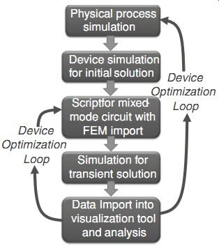
With traditional commercial TCAD tools, assuming a feasible use of the traditional TCAD approach, the simulation workflow can be visualized according to Fgr. 38.
With physical process simulation approach to obtain a new version of FEM device after even one parameter change the process steps must be completely redone. Any new variations of the mask parameters require re-run of the entire physical process deck again for deposition, etching, implantation, diffusion and other steps. If the change occur in the process recipe itself, then the calibration for the physical simulation steps is likely required too. This rather challenging task requires a substantial TCAD engineering effort to adjust the flow and introduce mask and mesh parameters especially for large HV analog devices.
After it’s generated by the process simulator, the FEM device file is imported into the simulation (with corresponding conversion of the activated species to donors and acceptors) to be solved in a static regime to obtain the initial condition.
The electrode conditions of this regime correspond to the initial conditions of this particular device in the circuit. At this step, the mesh usually needs to be redefined to eliminate unnecessary multiple nodes generated by the physical process simulation and to bring down the total mesh point count of the mixed mode circuit to a reasonable level. At the same time, the initial static solution for the mixed circuit is not always known and may require several iterations or even limit the type of problems that can be solved. Similar FEM files for the mesh and initial solution must be obtained for every different device type included in the mixed mode circuit, through tediously rerunning the entire physical process simulation flow ( Fgr. 38).
Fgr. 39 Mixed-mode simulation workflow with DECIMMTM [19]
Finally the mixed-mode simulation input file script is rewritten to import the FEM files and DC solutions. This concludes the mixed-mode simulation setup for the currently popular old generation TCAD tools implementing the traditional simulation approach.
During the mixed-mode simulation, the transient solution for a mixed-mode circuit generates output files that need to be imported into another program for visualization and data analysis. As well, new device/circuit optimization loops require repeating the entire tedious workflow ( Fgr. 38).
Apparently, such a cumbersome and time-consuming approach is rather challenging even for full-time dedicated TCAD professionals. So, it’s no wonder why TCAD simulation is not so popular among the majority of ESD engineers and analog IC designers, who desire rapid outcome and can afford to run TCAD only on part-time a casual basis. Thus, in spite of good accuracy of results obtained with a well-calibrated physical process simulation the methodology in general is impractical.
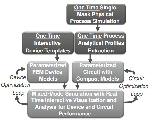
Fortunately for ESD engineers, a new tool DECIMM [19] has emerged over last few years. This tool completely replaces the physical process simulation by generating parameterized FEM devices in real-time during the mixed-mode simulation, using as input the diffused profiles and device templates. Similarly, fully parameterized circuits support mixed-mode simulation analysis, while real-time data extraction, visualization, and analysis are integrated in this single GUI simulator.
This simulation tool enables a revolutionary mixed-simulation workflow ( Fgr. 39) that combines procedures which must be accomplished for the entire process technology only once for each semiconductor device type. Thus, the mixed-mode analysis can be done for any circuit and FEM device parameters through a one-time input.
The first step of this approach is to obtain the diffused profiles for the given process. This can be done in several ways. For in-house processes, a single mask process simulation can be followed interactive extraction of the profile parameters supported by DECIMM tool. This is described below in more details. For foundries or in-house processes without physical process simulation flow data, alternative approaches consist in (i) receiving the profile information from the foundry; (ii) obtaining profiles from SIMS and SRP data by using external services and one-time test chips (iii) defining profiles manually using adjustments based on electrical results.
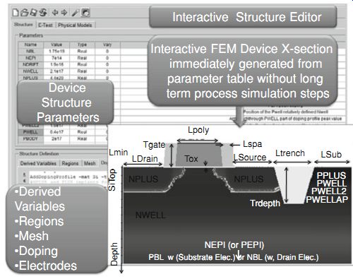
Fgr. 40 Interactive device parameterization and real-time FEM generation
in the DECIMM tool
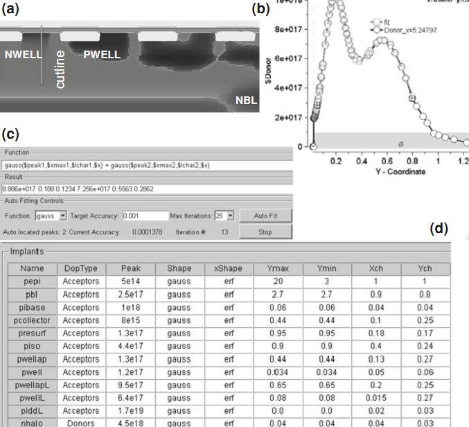
Fgr. 41 Process simulation cross-section for single mask diffused profiles
(a) and fitted analytical profiles (b) with extraction of implant parameters
(c) and the process definition table (d)
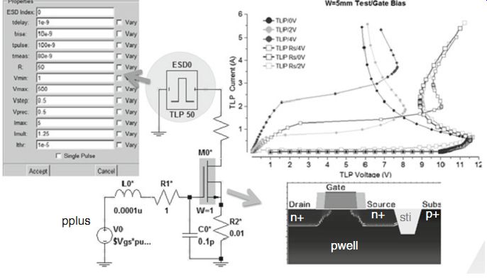
Fgr. 42 Automated mixed-mode analysis: circuit with automated TLP pulse source
demonstrates the tester parasitic effect for the source resistance
This IP ''investment'' enables developers to simulate the entire process technology. Creation of interactive FEM parameterized templates and circuit is sup ported by the DECIMM tool. The transient mixed-mode solution combined with real-time data visualization and analysis enable optimization loops at both circuit and device level ( Fgr. 39).
A few more details of this approach are provided below. The parameterized device generation is interactively defined in the tool by providing a set of physical device parameters supported by the interface and script-derived variables for related template regions and doping profiles ( Fgr. 40). Device regions and electrodes are set using an interactive device editor. All device regions, doping, and even semiconductor material parameters can be changed in the mixed-mode simulation since FEM generation is done in real-time, rather than by imported mesh and solution files. The parameterized device is equivalent to a device generated by the physical process simulation. The procedure of interactive automatic fitting and extraction from a single mask process simulation cross-section is illustrated in Fgr. 41.
In this example, a two-component Gaussian profile for the n-Well donor implant is obtained from the cutline after importing the single mask process simulation profile into the DECIMM tool. The two points on the cutline profile ( Fgr. 41b) define the fitting region. After running fitting iterations, the extraction results are shown in a fitted plot together with the set of extracted parameters for a two-peak analytical Gaussian profile ( Fgr. 41c). A table of diffused profiles is compiled with one-by-one cutline and extraction of the lateral and vertical profile parameters for each implant ( Fgr. 41d). This table shows a complete analytical representation of the process technology, combining the vertical Gaussian profiles for the implant and the error functions with the lateral profile parameters similarly extracted using horizontal cut lines ( Fgr. 41d). Unlike traditional process simulation, once the process parameterization implant table is obtained, any FEM device in the process can be generated in real-time using parameterized device templates.
Once the mixed-mode circuit is set, the simulation will run for any variation in physical devices or circuit parameters. An example of the TLP simulation for an NMOS device is presented in Fgr. 42.
There are several experimentally verified theorems that support this new methodology [20]. A 2D FEM device with analytical profiles is equivalent to an FEM device from calibrated process flow within a desired accuracy of ~5 %. The results are simulator-independent when compared to traditional TCAD tools for the same imported process files and the same set of activated models. Appropriate resultant implant profiles can be defined by a linear combination of diffused implant components using vertical Gaussian and lateral error functions. The parameterized FEM structure can be defined relative to real mask coordinates and device region boundaries-no mask bias is needed. Analytical diffused profiles extracted separately using the single mask approach can adequately generate FEM devices for the entire process.
So far, it has not been found that the user-friendly DECIMM tool [19] is indeed helpful in proceeding with simulation compared to the widely used empirical approach with its many costly re-design cycles. The material of the following sections will include many examples of the DECIMM-based mixed analysis involved to provide an in-depth understanding of the subject.
Top of page Article Index HOME