AMAZON multi-meters discounts AMAZON oscilloscope discounts
A significant progress in the predictability of system-level ESD design can be achieved by circuit simulation when ESD compact models are available for the on chip and off-chip ESD devices. Typically ESD compact models are not provided in a standard process design kit. However they can be developed using standard device models and sub-circuit components to model snapback regimes with avalanche breakdown and injection.
The sub-circuit components for ESD compact models include parasitic BJT structures, an avalanche current source, and saturation resistors. Development of the accurate snapback model is generally not an easy task. Due to complicated extraction methods for ESD current conditions, the construction of the scalable model requires advanced expertise in the field. One of the most helpful ways of developing a snapback model is to use the physical process and device simulation to generate the reference data for model extraction. Such an approach provides a significant acceleration of the extraction procedures under reasonable accuracy.
The generated compact models can be used for both ESD and functional simulations of large circuits, using standard circuit simulation tools such as HSPICE and Spectre, as well as for mixed-mode simulators, For example using DECIMMTM (see next section).
A number of original studies have been done to support the snapback model development [11-15] including the snapback ESD compact model for a low voltage NMOS [15]. This section presents an understanding of a general approach for custom ESD compact development principles to support the on-chip and off-chip ESD protection co-design. The following section is addressing the same goal based on the alternative approach of mixed-mode device-circuit simulation.
ESD Compact Model for LV Devices
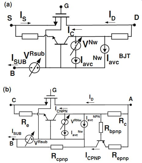
The simplest ESD compact model example is represented by the snapback NMOS device. The cross-section and the equivalent circuit representing the low-voltage NMOS device combines the standard NMOS represented by a non-snapback N-MOSFET circuit model, calibrated for a particular technology node, the parasitic n-p-n BJT represented by the transistor compact model and the avalanche current source ( Fgr. 31a). The bipolar device requires extraction of the current gain, forward ideality factor, reverse ideality factor, equivalent high-current collector resistor, and equivalent high-current emitter resistor [15].
The current-controlled voltage source VRSUB ( Fgr. 31b) represents the substrate resistance modulation analytically implemented as: where L, Ls, SWS and W are geometrical structure parameters ( Fgr. 31), and a_Rsub, b_Rsub, alfa_Rsub are extracted from the experimental data model parameters [15]. The avalanche breakdown current source component Iavc is described by:
[...] where the current components Ic and Ich, and Mb and Mch ( Fgr. 31) are the avalanche multiplication factors due to the bulk and channel regions with a high electric field in the vicinity of the drain-substrate junction depletion area.
The structure of the snapback PMOS model is essentially the same as that of the NMOS model above, with the changes from NMOS to PMOS and NPN BJT to PNP BJT.
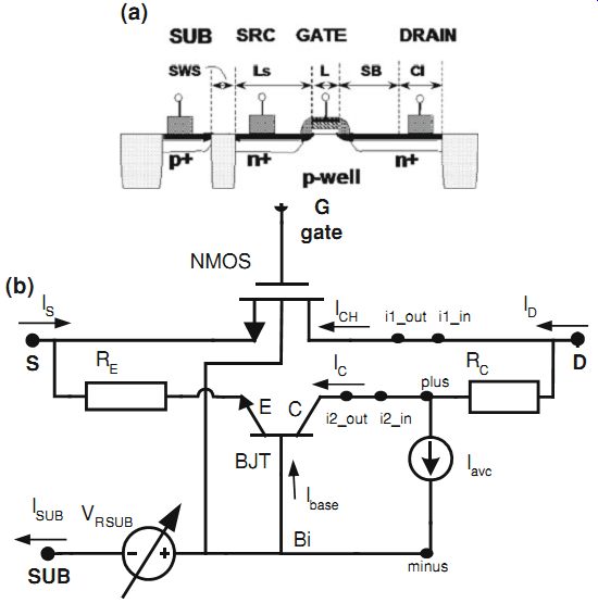
Fgr. 31 Cross-section and ESD layout parameters (a) and the equivalent circuit
(b) for the compact model with the avalanche current source AHDL of the snapback
NMOS device
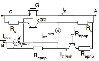
Fgr. 32 Equivalent circuit for an LVTSCR compact model
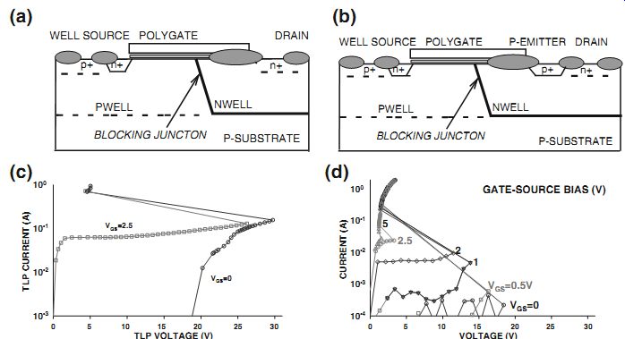
Fgr. 33 Simplified cross-section of 12 V NLDNMOS (a) and 12 V/20 V NLDMOS-SCR
(b) devices and corresponding measured TLP characteristics (sP = 100 ns, sR
= 10 ns) at different gate bias for W = 200 lm(c, d). Simulation of the Kirk
effect inside the NLDMOS device as a change of impact ionization region localization
for the condition of the avalanche breakdown (e) and the high current in snapback
mode (f).
The similar snapback NMOS module can be further reused in the compact model for the LVTSCR ESD device. To provide SCR-type positive feedback on the device level additional p-n-p BJT device is added in the sub-circuit.
Together with already included in the circuit parasitic NPN, this circuit creates a typical Ebers equivalent of an SCR. Additional components are the resistors:
Rbpnp to control the base resistance, Repnp to control the emitter resistance, and Rcpnp to control the collector resistance of the effective PNP device. The remaining components represent the part of the Pwell current (and associated potential) that does not contribute to the operation of the NPN device and has a rather large value.
Fgr. 34 Equivalent circuit of the snapback model circuits for NLDMOS (a)
and NLDMOS-SCR (b)
ESD Compact Model for HV Devices
ESD compact models for extended drain high voltage devices can be composed using the same sub-circuit approach. In case of NLDMOS ( Fgr. 33a) and NLDMOS-SCR ( Fgr. 33b) devices the extraction of several important parameters can be made using TLP I-V characteristics at different gate bias ( Fgr. 33c, d) [16]. The equivalent circuits of the snapback compact models for the NLDMOS and NLDMOS-SCR are similar to low voltage counterpart NMOS and NLVTSCR devices with one major exception.
For the NLDMOS device at high drain-source bias, the breakdown is initiated in the depletion zone of the NWELL-PWELL junction, as illustrated in the TCAD simulation shown in Fgr. 33e, f. Increasing the drain bias causes a significant voltage drop across the low-doped NWELL drain region, since it’s depleted of carriers. This is seen in the I-V characteristics after junction breakdown. When the high-field depletion region expands with increasing drain bias, it touches the highly doped N+ drain region. The conductivity of the NWELL region becomes completely over-modulated by the generated electrons and holes. This results in a shift of the maximum electric field (and impact ionization generation) toward the N+/NWELL interface. Often, this effect is attributed to the Kirk or base-push out effect [9]. In this regime, the parasitic bipolar device is activated, triggering the structure into snapback.
This behavior of the device has been used to develop circuit models for NLDMOS and NLDMOS-SCR structures operating in ESD conditions [16]. Initially, at low drain bias, the equivalent bipolar device and avalanche current source Iavc BJT, representing the impact ionization at the N+/NWELL junction, are not active.
The Iavc Nw avalanche current source describes the breakdown of the NWELL- PWELL junction and is expressed as Iavc Nw=MchIS, where Mch is the multiplication factor for the channel current. It’s given by the standard model
... where VNw represents the voltage drop across the carrier-modulated NWELL region.
It accounts for the modulation of NWELL resistance with the increase of injected carriers and is modeled as ...
In (1.4), lw and Aeff represent the effective length and cross-section of current flow in the NWELL region and are treated as fitting (extracted) parameters; q, ln, and vsat are the electron charge, mobility, and saturation velocity, respectively while Nd is doping. A similar equation is used for modeling the voltage source VR sub that represents the increase of substrate potential in junction breakdown conditions.
The avalanche current source Iavc BJT represents the shift of the avalanche region from the NWELL-PWELL to the N+/NWELL region, which leads to the activation of the parasitic bipolar structure. Iavc BJT is described as Iavc BJT = MBJT(kIS+IC). MBJT is described using a similar equation, as MCH (with different breakdown parameters) and k are parameters used to control the gate coupling effect in snapback operation.
Note that when Iavc BJT is activated, Iavc Nw consistently self-deactivates due to the bias VNw. This voltage drop reduces the effective bias across the NWELL-PWELL junction and, correspondingly, the avalanche multiplication that generates Iavc Nw.
Such model behavior is equivalent to the above-mentioned shift of the avalanche region inside the NWELL.
A properly calibrated compact model can provide rather good correlation of both the TCAD I-V characteristics calibrated to the experimental data and the circuit simulation characteristics generated by the model [16]. The model also accurately represents the breakdown and trigger behavior for different structure dimensions.
Similarly to LVTSCR, the NLDMOS-SCR model can be constructed by attaching a PNP bipolar device to the NLDMOS snapback model, as shown in Fgr. 34b. The equivalent emitter and base resistance Repnp and Rbpnp are used to control the activation and the high-current operation of the equivalent PNP transistor. Rcpnp represents the PWELL resistance and substrate current flow that does not contribute to the operation of the NPN device.
An example of simulation with ESD compact models is represented by a simplified schematic ( Fgr. 35a) of an open drain driver circuit, which combines HV NLDMOS and NLDMOS-SCR structures. The NLDMOS device has an attached 30 kX gate resistor to mimic the dynamic coupling load from the driver circuit. In ESD conditions, depending on the circuit and structure parameters, the ESD current can discharge either through the NLDMOS-SCR ESD protection clamp or through the NLDMOS device. As can be seen from the comparative analysis of the waveforms ( Fgr. 35b, c), two different scenarios are realized.
When RGATE =10kX, under given circuit parameters for a 2 kV HBM, the gate coupling on the NLDMOS-SCR gate is sufficient to provide the early turn-on. As a result, the SCR clamp takes over the ESD current ( Fgr. 35b). On the contrary, in the case of insufficient gate coupling where RGATE =1kX, the clamp does not turn on and the current path is formed through the 5 mm NLDMOS device ( Fgr. 35c).
Thus, depending on the circuit parameters and the HBM pulse amplitude, the critical regime can be determined as a condition of where the current changes direction in the turning-on circuit from the SCR clamp path to the NLDMOS path.
If the current through NLDMOS is uniform, the high-current operation will be non-destructive. However, in a real 3D situation, the local snapback turn-on might result in irreversible failure [17].
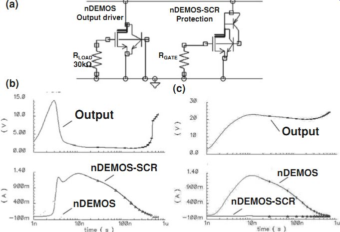
Fgr. 35 Simplified schematic of ESD protection for open drain output driver
(a) voltage current waveforms for two values of RGATE-10 kX (b) and 1 kX (c),
representing two possible circuit designs.
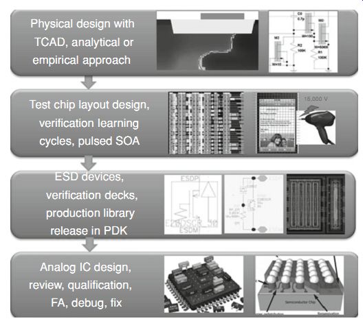
Fgr. 36 Illustration of the industrial ESD development workflow for new technology
process development.
A similar scenario of competition between the snapback clamp and array turn on can result from the substrate potential effect. The substrate coupling technique is also one of the most useful methods in controlling ESD devices [18].
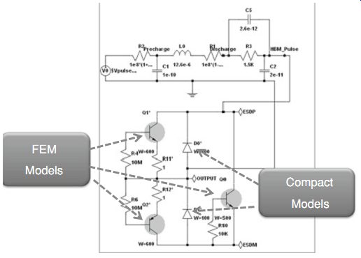
Fgr. 37 Illustration of the mixed mode simulation approach with FEM devices.