AMAZON multi-meters discounts AMAZON oscilloscope discounts
Most diode detectors also include an automatic volume control (AVC) circuit, along with the basic detector discussed in the previous section. Automatic volume control is a fairly elaborate function within radio receivers. Its purpose is to maintain a constant audio output, or volume, in the face of possible changes in signal strength due to abnormal propagation conditions. Signal fades and build-ups are the obvious results of these irregularities in propagation. It would be most disconcerting for the listener to have to continually adjust the volume on his receiver in order to compensate for a program becoming suddenly too loud or faint. Therefore, automatic volume control is added to virtually all radio receivers.
SUMMARY OF ILLUSTRATIONS
A total of eight circuit diagrams and seven waveform diagrams are used to illustrate the various actions in the operation of a diode detector with AVC. The first two circuit diagrams (Figs. 5-1 and 5-2) show successive negative and positive half-cycles of unmodulated radio frequency signal current being received and detected by diode detector V1 (this tube is an integral part of the total AVC circuit). Certain DC voltages come into existence when this detection occurs. These are shown as the three detected voltages on the upper plates of capacitors C2, C3, and C4, and also as the AVC voltage on the upper plate of capacitor C5. The electrons which constitute these detected voltages come originally from the plate current of the tube. Consequently they, too, are shown in green.
Fig. 5-3 shows negative and positive half-cycles of tank voltage and current, and also of detector plate current and AVC voltage.
The plate current leaves the tube in the form of pulsations at the signal frequency. Filter capacitor C2 bypasses these pulsations to ground. This bypassed, or filtered, RF current is shown in dotted blue.
The next two circuit diagrams (Figs. 5-4 and 5-5) show the actions occurring in the audio half-cycles which precede a modulation trough and peak. Also, Fig. 5-6 shows a modulated wave form for each condition. It also portrays the pulsations in plate current, the negative audio and AVC voltages, and finally, a sine-wave representation of the current which must flow through an AVC resistor (such as R4) when RF signals are being demodulated.
The next two circuit diagrams (Figs. 5-7 and 5-8) show the voltage-current conditions while a carrier signal is fading. The waveform diagrams in Figs. 5-9 and 5-10 show the changes occurring in the carrier signal, the resultant audio voltage, and finally the change in AVC voltage during a carrier fade.
The last two circuit diagrams (Figs. 5-11 and 5-12) show the voltage-current conditions while a carrier signal is building up.
The associated waveform diagrams of Figs. 5-13 and 5-14 illustrate the changes occurring in the carrier signal, the audio voltage, and the AVC voltage during a carrier build-up. Fig. 5-15 is a graphical representation of the audio voltage developed across output resistor R2 during a period of carrier fade and a period of carrier build-up.
Some of the important truths the reader should expect to learn from these diagrams and the text include:
1. The changes in audio voltage on capacitors C2, C3, and C4 from modulation peak to trough, and what causes them.
2. Why the AVC voltage on capacitor C5 does not change be tween modulation troughs and peaks.
3. What causes an audio current to flow up and down in out put resistor R2.
4. What causes the AVC current to flow back and forth in AVC resistor R4 at the audio frequency, and why this current flow does not change the amount of AVC voltage stored on capacitor C5.
5. What causes the negative AVC voltage to decrease during a carrier fade and to increase during a build-up.
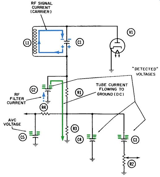
Fig. 5-1. The AVC circuit-negative half-cycle of unmodulated RF.
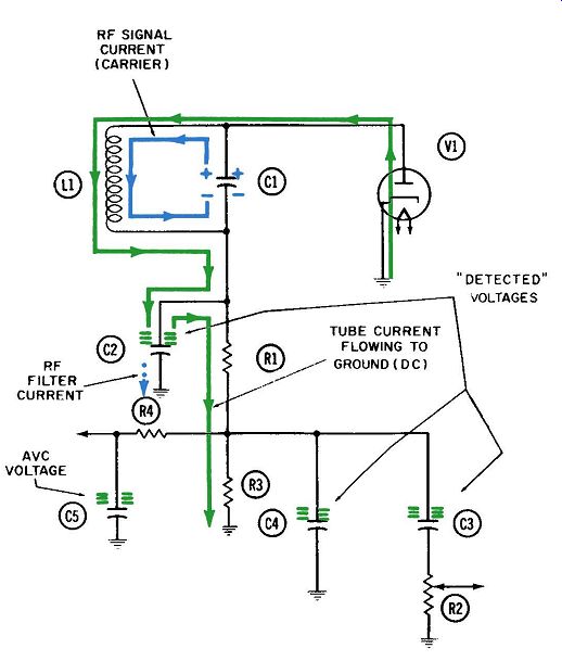
Fig. 5-2. The AVC circuit-positive half-cycle of unmodulated RF.
CIRCUIT DESCRIPTION
The components which make up this circuit, and their functional titles are:
R1-Filter resistor (works in conjunction with C2).
R2-Audio-output resistor.
R3-Primary load resistor.
R4-AVC resistor.
C1-RF tank capacitor.
C2-RF filter capacitor.
C3-0utput coupling capacitor.
C4-Additional RF filter, or bypass, capacitor.
C5-AVC storage capacitor.
L1-RF tank inductor.
V1-Diode tube.
Five electron currents are at work in this over-all circuit. They are:
1. Radio or intermediate-frequency tank current (solid blue).
2. Pulsating radio or intermediate-frequency DC flowing through the detector (green).
3. AVC filter current (also in green).
4. Modulation signal, usually called audio (red).
5. Radio-frequency filter currents (dotted blue).
Voltage levels, both for audio and for automatic volume control, are shown by green minus signs. There are three kinds of time periods, which might be referred to as cycles, that are important in understanding this circuit. These periods are the short time required for one RF or IF cycle, the somewhat longer time for one modulating cycle, and the much, much longer time required for signal fades or build-ups. A typical intermediate frequency (IF) in broadcast receivers is 455 kilocycles per second. Thus the time required for one IF cycle is 1/ 455,000 second, or slightly more than two microseconds.
If the audio tone being demodulated is middle C, then its frequency will be 256 cycles per second. Thus the time for one such audio cycle is 1/256 second, or about four milliseconds. This is 4,000 microseconds-about two thousand times longer than the time of one IF cycle.
Even this is short compared with the time required for a signal to completely fade or build up. The latter may take several seconds or even minutes. Thus, many hundreds or even thousands of audio cycles may occur during one fade or build-up.
These relative time values are important to understanding demodulation and the automatic control of volume.
In order to depict one complete audio cycle in the accompanying diagrams, it would be necessary to show the 2,000 IF cycles occurring. This would hardly be practical. Likewise, to show a complete signal fade followed by a build-up, we would have to show several thousand audio cycles-and consequently many millions of IF cycles.
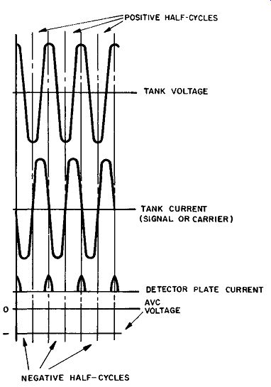
Fig. 5-3. AVC circuit waveforms when un modulated RF is being received.
As is true with any vacuum tube, a closed path must be avail able between plate and cathode of the detector diode in order for detector current to flow. This path includes coil L1 and resistors R1 and R3. The green line has been chosen to represent detector current; it completes a path from plate to ground by flowing through L1, R1, and R3.
R1 and C2 together act as a radio-frequency filter. Resistor R3 and capacitor C4 act as an additional RF filter. Resistor R2 and capacitor C3, in conjunction with R3 and C4, develop an audio-voltage output from the detector or demodulator stage.
Resistor R4 and capacitor CS are the two components which provide the necessary compensation for varying signal strengths.
Without them, the remainder of the circuit would continue to function as a fairly elaborate diode demodulator. In order to understand the AVC function, it is necessary to begin with the diode detector and to consider how it operates to detect, or de modulate, an incoming radio-frequency signal.
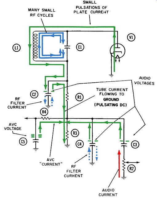
Fig. 5-4. Operation of the AVC circuit-audio half-cycle pre ceding a modulation
trough.
CIRCUIT OPERATION
In Fig. 5-4 when a modulation trough is occurring, we see two green minus signs on the upper plate of filter capacitor C2.
Between the lower plate of this capacitor and ground, the dotted blue arrows indicate current flow in both directions. This cur rent, which is flowing at the basic radio frequency, represents the RF pulsations being filtered out of the detector current be fore it continues its journey back to the cathode.
Capacitor C2 is of such a size that its reactance at this particular radio frequency will be substantially less than the resistance of the alternate path available to the detector current.
This path is through the series combination of R1 and R3 to ground.
Figs. 5-4 and 5-5 each cover a period which includes many RF cycles. The reader should recognize that this filtering current flows downward when a pulsation of detector current flows onto the top plate of C2, and that it flows upward in the interim before the next pulsation occurs.
When a detector pulsation of current is small, as it is near a modulation trough, only a small filtering current must flow. On the other hand, when a pulsation is large, as it is near a modulation peak (Fig. 5-5), a large amount must flow.
Although this filtering current is driven by the pulsations of detector current (shown in green), the filtering current is shown in dotted blue in order to help clarify the actual closed path of detector current from plate to ground. While the energy in the individual pulsations is passed across the capacitor plates, the electrons which compose the detector current form a pool of negative voltage on the upper plate of C2 until they can escape down ward through R1 and R3 to ground and the cathode.
This pool of electrons on the upper plate of C2 constitutes the first appearance of the audio voltage in a receiver system. Receivers are customarily analyzed in the order in which a signal progresses through from antenna to speaker. Until this detector stage is reached, no audio voltage has been generated in the system.
In Fig. 5-4, the amount of negative voltage on capacitor C2 is indicated by the two minus signs. In Fig. 5-5 this negative voltage has been greatly increased, as indicated by a total of ten such signs. These two figures constitute one whole cycle of the audio, or modulating, voltage. The voltage on this capacitor indicates the rise and fall of the audio voltage in accordance with the peaks and troughs of the modulating envelope. During each half-cycle of the audio voltage, many hundreds or even thousands of pulsations of detector current will be coming into the capacitor.
The waveforms of Fig. 5-6 should be studied in conjunction with Figs. 5-4 and 5-5. Note that the sine wave of audio voltage in Fig. 5-6 is below the reference line of zero voltage at all times.
In other words, the audio voltages which appear simultaneously on capacitors C2, C3, and C4 are negative at all times; and they fluctuate from their low negative value at the modulation troughs, to a high negative value at the modulation peaks.
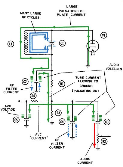
Fig. 5-5. Operation of the AVC circuit-audio half-cycle pre ceding a modulation
peak.
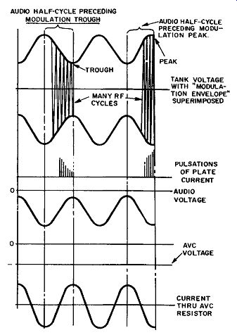
Fig. 5-6. AVC circuit waveforms when modulated RF is being received.
The electron current which flows downward through R1 and R3 is a pulsating unidirectional current, but the pulsations are occurring at the audio frequency. The least current flows when the voltage on C2 is lowest, during the modulation trough. Conversely, the most current flows when the voltage on C2 has its highest value, during the modulation peak.
Since an audio current flows through resistors R1 and R3, an audio voltage is developed across them. This is in accordance with Ohm's law. It is desirable for R3 to be considerably larger than R1, so that most of this audio voltage will be developed across R3. The reason for this will b. apparent from analysis of the function of resistor R2 and capacitor C3. These two are in series with each other, and the series combination is in parallel with R3. R2 is a variable resistor across which the output audio voltage is developed. This potentiometer is commonly used as the volume control in receiver systems.
Capacitor C4 serves primarily as an additional radio-frequency filter, on the likely assumption that the combination of R1 and C2 will not do a thorough job of filtering the RF pulsations out of the detector current and into ground.
The combination of C3 and R2 is critical because the two develop the output audio voltage for the next amplifier stage. The product of these two components must give a short time-constant when compared with the lowest audio frequency being demodulated. When this short time-constant condition has been met, an alternating current at the audio frequencies will flow up and down through resistor R2. This current will be drawn upward as electrons flow away from the upper plate of capacitor C3 during the modulation trough, as indicated in Fig. 5-4. Conversely, the current will be driven downward through R2 as electrons flow onto the upper plate of C3 during the modulation peak, as indicated in Fig. 5-5.
This two-way current through R2 is the first appearance in the receiver of alternating current at the audio frequencies. The audio current which flows through R1 and R3 is unidirectional. In other words, it is DC which pulsates at the audio frequencies. Frequently this current is called pure DC with an alternating component superimposed on it. Both concepts are correct, and the reader should use the one that is clearer to him.
The alternating current through resistor R2 develops an audio voltage across it, in accordance with Ohm's law. This voltage then becomes the output of the detector stage. By moving the arm of the potentiometer to the various points on the resistor, it is possible to apply any given percentage of this output audio voltage to the grid of the first amplifier stage. By this means, the receiver volume can be adjusted to any desired level.
Although the voltage levels on C3 and C4 follow the changes occurring on C2, the two are slightly lower than the voltage on C2. The amount of reduction in audio voltage is an accurate reflection of the relative voltage drops occurring across R1 and R3, respectively. The voltage drop across R1 is a loss, which is made acceptable by the filtering achieved from adding R1 and C2 to this circuit.
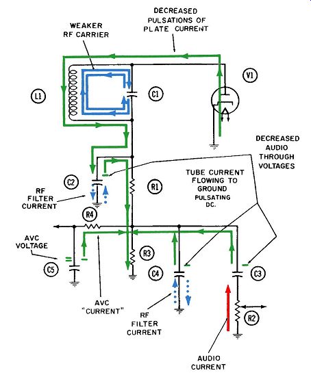
Fig. 5-7. Operation of the AVC circuit-modulation trough during a carrier
fade.
Resistor R4 and capacitor CS form the AVC filter combination.
In order to understand how these components perform, it is desirable to visualize the current through R4, the voltage on the upper plate of CS, and their interrelationship with the audio voltage on C4 and C3. Since the voltage level on these capacitors is rising and falling in accordance with the modulation, we can visualize an average voltage value for a whole modulating cycle.
The detected voltages shown in Figs. 5-1 and 5-2, when the carrier is unmodulated, are a fair approximation of what this average value would be. During the modulation trough of Fig. 5-4, the voltage level on these capacitors is below this average level.
Conversely, it is above the average value during a modulation peak in Fig. 5-5.
Even with changes in percentage of modulation, this average voltage level on the capacitors will not change, although the amounts of voltage above and below the average will. For in stance, with a very low percentage of modulation impressed on the carrier wave, the capacitor voltage during the modulation trough will be only slightly below average. On the other hand, during a modulation peak it will be an equal percentage above the average level.
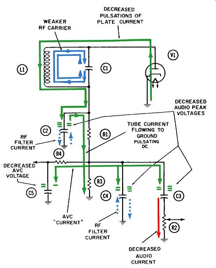
Fig. 5-8. Operation of the AVC circuit-modulation peak during a carrier
fade.
Let us consider how capacitor CS acquires its charge of negative voltage, as indicated by the series of green minus signs. If there were no modulation at all on the carrier signal, then the average voltage levels on C3 and C4 would be quickly achieved and maintained because of continued detection of the unmodulated carrier. Under this condition, electron current would flow from the upper plates of C3 and C4, through resistor R4, to the upper plate of C5. Eventually CS would become charged to the same average value of negative voltage. This leads us to an important point in the operation of AVC circuits ( and in under standing them)-namely, the AVC capacitor will charge to the average value of the audio voltage.
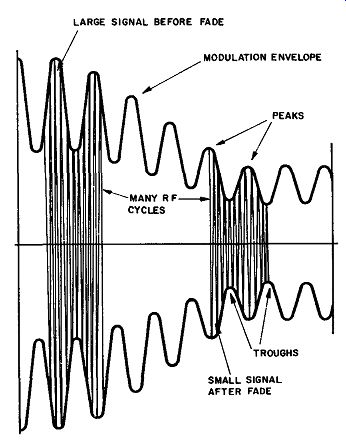
Fig. 5-9. The modulated carrier during a signal fade.
Once the reader visualizes that this can and does happen to an unmodulated carrier, only one more step is required to demonstrate that this principle still holds where there is some modulating voltage on the carrier signal. Figs. 5-4 and 5-5 are useful for demonstrating this point. During the modulation trough depicted by Fig. 5-4, electron current (shown in green) will flow out of AVC capacitor C5 and toward those points of lesser negative voltage on C3 and C4. During the modulation peak depicted by Fig. 5-5, a greater negative voltage exists on C3 and C4.
Now electron current flows awa11 from, these capacitors, toward the AVC capacitor. The voltage on this capacitor has remained substantially unchanged during the entire cycle.
The reason the voltage level on the AVC capacitor does not change during an individual cycle of audio voltage can best be understood by calling on the time-constant concept. When a resistance in ohms is multiplied by a capacitance in farads, the resultant product has the dimensions of time and is measured in seconds. In a long time-constant RC combination, its product is a long time, in comparison with the duration of one cycle of the frequency under consideration. The lowest frequency of audio voltage in a normal receiver might be in the neighborhood of 100 cycles per second, so that the time for one cycle is .01 second.
(Time for one cycle is always the reciprocal of the frequency, or T = 1/f.) AVC resistors and capacitors are very large components. Typical values for R4 and C5 would be 2 megohms and .05 micro farad, for example.
Calculating the time constant of this combination, we find that:
T=RXC = (2 X 1QH) X 5 X 10^-8 = 0.1 second
One-tenth of a second is certainly a long time, in comparison with the one-hundredth of a second of the longest audio cycle considered above.
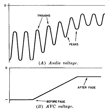
Fig. 5-10. The audio and AVC voltage changes during a signal fade.
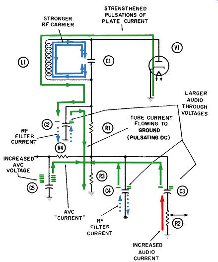
Fig. 5-11. Operation of the AVC circuit-modulation trough during a carrier
build-up.
The AVC capacitor is much larger than C3 (which is much larger than C4). Hence, many more electrons are required to charge the AVC capacitor to the average voltage level than are required by C3 and C4. Because the AVC resistor also is large, only a minute amount of electrons will be driven back and forth through it as the voltage levels on C3 and C4 change in accordance with the modulation peaks and troughs. This small amount of electron traffic in and out of C5 will be insignificant in comparison with the electrons stored there. Consequently, the AVC voltage-which is the negative voltage stored on the upper plate of AVC capacitor C5--does not change with the audio or modulating voltage. This is an important point in understanding automatic volume control.
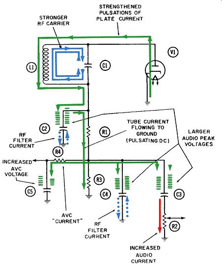
Fig. 5-12. Operation of the AVC circuit-modulation peak during a carrier
build-up.
The AVC line connected to the junction of R4 and C5 leads directly to the control grids of one or more RF amplifier tubes.
The carrier signal must be processed through these tubes before it reaches tuned tank L1-C1. Hence, this increased negative voltage shows up as a larger negative bias on the grids of these tubes and reduces their amplification, to compensate for the stronger signal.
A signal fade or build-up may take place over a period of several seconds. During this time, many hundreds of cycles of audio voltage will probably occur. The audio current (shown in red)
which flows back and forth through R2 will of course continue to do so during this time. However, the voltage on C5 can only be changed by the current through resistor R4. This resistor, along with R3, provides the only path to ground for the electrons which make up the AVC voltage on C5. The only way this voltage can be decreased or increased is for electrons to empty out through R4, or for more electrons to come in through that path.
In the example shown, when a signal build-up occurs more electrons must flow into C5 during the modulation peaks than flow out during the modulation troughs. This flow continues until the AVC voltage has become stabilized at the new average audio voltage. During this interim, the current flowing through R4 to the left in Fig. 5-12-will exceed the current flowing to the right in Fig. 5-11. Thus, although two-way current continues to flow through the AVC resistor at the audio frequencies, its amount varies between individual half-cycles. In this way, the AVC voltage is automatically kept at the average value of audio voltage coming from the detector.
CIRCUIT ACTIONS DURING A CARRIER FADE
Fig. 5-9 is a simplified representation of a modulated carrier signal undergoing a fade, or reduction in signal strength, because of abnormal propagation or atmospheric conditions. Fig. 5-10 shows the resultant reduction in audio voltage after detection or demodulation. It is important to note that individual audio cycles are larger before the fade. Also note the more obvious fact that the average value of the audio voltage decreases from a high to a low negative value during the fade. The AVC voltage line in this figure represents the negative voltage stored on capacitor C5 in Figs. 5-7 and 5-8. This line faithfully reflects the average value of audio voltage.
Fig. 5-7 shows the relative sizes of the audio and AVC voltages at the moment of a modulation trough, after the carrier has faded.
Fig. 5-8 shows the same voltages at the moment of a modulation peak. Compare these voltages with those that existed at the same points before the carrier faded (Figs. 5-4 and 5-5). You will see that the audio and AVC voltages are both lower. However, the amounts of AVC voltages indicated in Figs. 5-7 and 5-8 are in tended to be equal, because the AVC voltage does not change from modulation trough to peak. This is due to the long time constant nature of the R4-C5 filter combination, as previously discussed.
During a carrier fade, the AVC current which flows through resistor R4 reduces the number of electrons stored on capacitor C5. This is normally a minute two-way current that flows at the audio frequency. During a modulation trough this current flows to the right, as shown in Figs. 5-4, 5-7, and 5-11, because the momentary audio voltage at the right end of the resistor is more negative than the stored AVC voltage at the left. Electrons will always flow from an area of higher to one of lower negative voltage as long as a conducting path is provided. During a modulation peak this current flows to the left, as shown in Figs. 5-5, 5-8, and 5-12.
Under normal conditions, the amount of AVC current which flows to the right during a modulation trough will just equal the amount which flows to the left during a modulation peak. How ever, when a carrier fade is occurring, these two components of current are no longer equal. More current flows to the right during the trough half-cycle than flows to the left during the peak half-cycle. This inequality will continue until the fade has been completed, and in this way the AVC voltage will "discharge" electrons until it again equals the average value of the audio voltage.
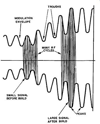
Fig. 5-13. The modulated carrier during a period of signal build-up.
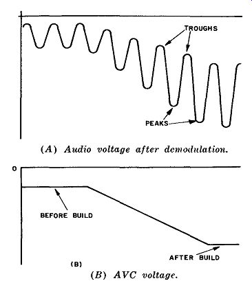
Fig. 5-14. The audio and AVC changes occurring during a period of signal build-up.
(A) Audio voltage after detection. (B) AVC voltage.
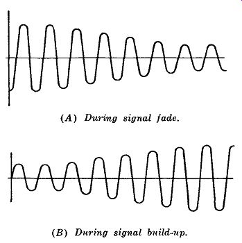
Fig. 5-15. The audio output voltage during a signal fade and a signal build-up.
(A) During signal fade. (B) During signal build-up.
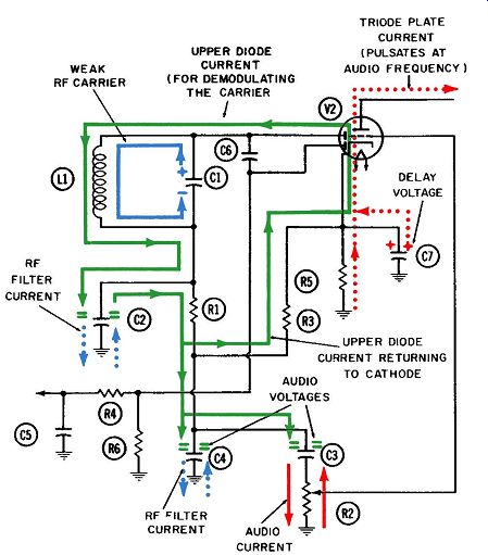
Fig. 5-16. The delayed AVC circuit-weak-signal operation.
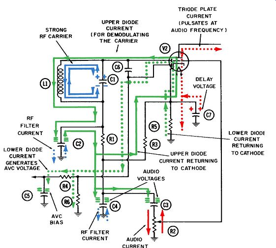
Fig. 5-17. The delayed AVC circuit-strong-signal operation.
CIRCUIT ACTIONS DURING A CARRIER BUILD-UP
Fig. 5-13 shows a simplified representation of a modulated carrier signal undergoing a build-up, or increase, in signal strength. Fig. 5-14 shows the resultant increase in audio voltage after demodulation, and also the increase in negative AVC voltage as a result of this build-up in signal strength. As in the case of the fading signal, the AVC voltage accurately reflects the average value of the audio voltage.
Fig. 5-11 shows the audio and AVC voltage during a modulation trough, after a carrier build-up. By comparing these voltage pictures with the same voltages in Fig. 5-4, you can see that the build-up in carrier strength has caused the audio and AVC voltages to go more negative.
Fig. 5-12 shows these voltages to be larger than their counter parts in Fig. 5-5 before the carrier build-up. Between the modulation trough of Fig. 5-11 and the peak of Fig. 5-12, however, the AVC voltage itself does not change. The AVC current flowing through resistor R4 again provides the mechanism by which the AVC voltage becomes stabilized at the average value of audio voltage.
AUDIO-OUTPUT VOLTAGE
Fig. 5-15 shows the audio-output voltage developed across potentiometer R2 as the audio current (shown in red) is driven up and down through R2. As indicated in Figs. 5-4, 5-7, and 5-11, this current flows upward during modulation troughs. During modulation peaks, it goes downward, as shown in Figs. 5-5, 5-8, and 5-12. Excess electrons from the detector tube flow onto the upper plate of capacitor C3 during modulation peaks, driving an equal number away from the lower plate and down through the resistor. (This is the basic capacitor action.) As these excess electrons flow away from the upper plate of C3 during a modulation trough and discharge to ground through R3, an equal num-her will be drawn upward through R2 to the lower plate of C3.
During a carrier fade, less audio current will flow and there fore less output voltage will be developed across resistor R2, as indicated in Fig. 5-15A. The resultant reduction in volume would be undesirable to the listener. However, if we connect the grid of a previous RF amplifier tube to the AVC voltage point on capacitor C5, the lower AVC voltage will reduce the negative grid bias on the RF amplifier tube. This will increase the amplification of the signal and thus largely nullify the effects of the fading signal.
Likewise, during a carrier build-up the spread between peak and trough voltages on capacitor C3 is greater and more audio current will flow in output resistor R2. According to Ohm's law, the voltage developed across a resistor is proportionate at all times to the current flowing through the resistor. Thus, the audio output voltage increases as the carrier strength builds up. This higher voltage, shown by Fig. 5-15B, may increase the loudness to the point where it is most unpleasant to the listener.
When the higher negative AVC voltage on capacitor C5 is connected to the control-grid circuit of a previous amplifier tube, the negative grid bias of the tube will be increased and its amplifying properties reduced. This reduces the total amplification of the signal and largely nullifies the undesirable effects which would otherwise result from the stronger signal.
DELAYED AVC
Figs 5-16 and 5-17 show two modes in the operation of a circuit designed to provide delayed automatic volume control.
There are considerable similarities between this circuit and the on~ shown previously. To accentuate these similarities, individual components having identical functions in the two circuits have been assigned the same names. The component names and functions are:
R1-Filter resistor.
R2-Audio-output resistor.
R3-Primary load resistor.
R4-AVC resistor.
C1-RF tank capacitor.
C2-RF filter capacitor.
C3-0utput coupling capacitor.
C4-Additional RF filter capacitor.
C5-AVC storage capacitor.
L1-RF tank inductor.
Additional components in the delayed AVC circuit, which were not present in the previous AVC circuit, are: RS-Cathode filter capacitor.
R6-AVC return resistor.
C6-Isolating and coupling capacitor between the two diode plates.
C7-Cathode filter capacitor.
V2-Dual-diode/triode tube.
Principles of Operation:
Delayed--AVC allows us to eliminate the AVC on weak signals, but to enjoy its benefits when the incoming signal level reaches a predetermined strength. These objectives are accomplished by using separate diodes for signal demodulation and for automatic volume control. Recall that the electron current through the single diode in the preceding example was eventually used to provide an audio-output voltage as well as an AVC bias voltage.
Each diode plate in tube V2 operates independently from the other, and also independently from the triode operation within the same envelope. The fundamental principle of diode operation prevails in either case--that whenever a diode plate is more positive than the cathode, electrons will be drawn across the open space between the two electrodes.
Both diode plates are driven by the same alternating tank voltage. The tank current associated with this tank voltage is shown circulating between the inductance and capacitor within the tank. The half-cycle in Fig. 5-16 represents operation during a weak signal. At the moment shown, the tank current is flowing downward through L1 and thus delivering electrons to the lower plate of capacitor C1, making it negative and the upper plate positive.
This positive voltage is coupled directly to the upper diode plate and capacitively (by means of C6) to the lower diode plate.
Even with a weak RF or IF signal applied from the tank, the upper diode plate will draw some electron current on the positive half-cycles. This diode current, shown by the solid green lines, follows a similar path as the diode current in the previous example, with one important difference. After flowing through resistor R3, it goes directly to the cathode rather than ground.
This manner of connecting R3 to the cathode assures that the signal will be detected, even with weak signals. Since the multiple tube has a common cathode and since cathode biasing is used in connection with the amplifying function of the tube, the cathode is necessarily placed at a positive voltage. This voltage persists as long as electron current flows through the tube.
Depending on the requirements of the particular circuit, this positive cathode voltage might have any reasonable value--but for convenience, let us assume it is +3 volts. This becomes the amount of delayed AVC the circuit is using. The lower diode plate is returned to ground through resistor R6. So this diode plate will assume a reference voltage of zero. The alternating voltage resulting from the IF oscillations in the tuned tank is coupled to this diode plate by capacitor C6. As a result, the diode plate voltage will vary in either direction from this zero reference value.
In the weak-signal example shown in Fig. 5-16, the IF oscillations are considered small enough that they never raise the lower diode plate any higher than +3 volts. Consequently, no electron current can flow between the cathode and this plate, and no automatic-volume-control voltage will be developed.
In the strong-signal example of Fig. 5-17, the IF oscillations are large enough that they raise the lower diode plate well above +3 volts on each positive peak. Fig. 5-17 depicts one such positive peak occurring. As a result, the lower diode plate is now more positive than the cathode, and conduction occurs. The complete path of this electron current, shown in dotted green, is from cathode to lower diode plate within the tube, then downward to the junction of the two AVC resistors R4 and R6. The ultimate destination is of course back to the chassis and then to the cathode. However, resistor R6 is made large enough to impede this flow and divert some of the electrons into resistor R4. Eventually a pool of electrons collects on the upper plate of capacitor C5. These accumulated electrons become the AVC voltage, which is applied to one or more control grids of the preceding RF (or IF) amplifier tubes.
This negative AVC voltage increases as the signal becomes stronger and vice versa, in the same manner shown in earlier figures of this section. Because of the similarity in function be tween these two circuits, a detailed analysis of AVC will not be repeated here.