AMAZON multi-meters discounts AMAZON oscilloscope discounts
The diode detector is one of the simplest and most widely used circuits for detection of a carrier wave. The term "detection" is frequently used synonymously with "demodulation"-particularly whenever some modulation is imposed on the radio-frequency carrier wave at the transmitting source. The detector circuit produces a steady, or DC, voltage which will at all times be proportionate to the strength of the carrier wave. In fact, this voltage depends on the carrier wave for its existence. Consequently, if the carrier signal is turned on and off by keying the transmitter, the detector circuit will provide a means of knowing this at the receiver, and therefore a means of "reading" the keying.
CIRCUIT DESCRIPTION
Figs. 4-1 and 4-2 show the two half-cycles of operation of the diode detector. The circuit components and their functional titles are:
R1-Diode load resistor.
C1-RF tank capacitor.
C2-Coupling capacitor.
T1-Output IF transformer.
V1-Diode tube.
There are only two main families of currents at work in this circuit:
1. Radio-frequency alternating currents (blue).
2. Unidirectional tube current (red).
The radio-frequency tank consists of transformer T1 and capacitor C1. This circuit is resonant at the particular radio frequency being received. An oscillation of electrons will be built up in this tank and be sustained by another RF current which exists at the same frequency in the primary winding of the transformer. Both currents are shown in blue.
RF TANK CURRENT
Fig. 4-3 shows a series of sine waves representing the radio frequency voltage and current in the tank. Unless otherwise stated, such a voltage sine wave normally applies to the voltage at the top of the tank; this is the point of coupling to the plate of the diode detector. The first half-cycle is centered at the instant of maximum negative voltage, as indicated in Fig. 4-1 by the blue minus signs on the top of plate tank capacitor C1. The blue line indicating electron current is shown during this half-cycle as flowing upward through the transformer secondary, thus delivering electrons into C1.
The tank voltage is represented by the plus and minus signs on the upper plate of C1 in Figs. 4-1 and 4-2. It drives an external current (shown in blue) up and down through diode load resistor R1. When this tank voltage is at its maximum negative value midway in the negative half-cycle, the electrons in this external current will be flowing downward through R1 at their maximum rate.
By the same token, when the tank voltage is at its maximum positive value midway in the positive half-cycle, the external current electrons will be flowing upward through R1 at their maximum rate. This will cause the top of the resistor to reach its maximum positive voltage, which is just high enough to over come the negative voltage caused by the accumulation of electrons on the right plate of C2. As a result, the diode can again conduct.
The normal path for this external current driven by the tank current is up and down through diode load resistor R1. There is a simple rule of thumb for determining the instantaneous polarity of a voltage associated with any current flow. Recall that current is nothing more than electrons in motion; also, that all electrons have a negative charge and are therefore repelled by each other and by negative voltages in general. So, in flowing through a conductor, electrons always head toward a point of more positive (less negative) voltage than the point from which they are leaving. Since the lower end of the resistor is tied to ground, it will always be at zero voltage. Therefore, when electrons flow down- ward through R1, as they do in Fig. 4-1, the driving voltage at the top of the resistor must be negative. Conversely, when they flow upward as in Fig. 4-2, this driving voltage must be positive.
UNIDIRECTIONAL CURRENT
Diode tubes have one important characteristic-when their plate voltage is more positive than their cathode voltage, electrons will cross the evacuated space from cathode to plate. This condition is fulfilled during a portion of the second half-cycle (but not during all of it), and electron current is shown in red crossing the tube. The complete path for this current is from cathode to plate and downward through diode load resistor R1 to ground, then through ground and back to the cathode. During its journey through the tube and to the top of the resistor, this DC current is pulsating at the basic radio frequency. Because of the delay in entering and passing through the resistor, the electrons from the detector tube accumulate on the right plate of capacitor C2.
Here they form a constant negative voltage, as indicated by the red minus signs on the capacitor. Some electrons flow into this pool during each pulsation from the detector, and an equal number flows out during the entire cycle. The latter flow is pure rather than pulsating DC.
CIRCUIT OPERATION
It is important to distinguish between the two different currents which flow through the diode load resistor. The current just discussed, along with its associated negative voltage on the right plate of capacitor C2, applies a fixed negative voltage to the plate of the diode. Before the diode can conduct, the other current (shown in blue) must first overcome the fixed negative voltage.
This will occur only during that portion of the positive half-cycle when this current is flowing upward at or near its maximum rate.
During these moments, it will exceed the amount of fixed current which regularly flows downward through the resistor each time the diode conducts. The net result of the two opposing voltages is a small, momentary positive voltage at the diode plate, permitting more tube current to flow. These moments occur midway in each positive half-cycle. Fig. 4-3 shows a small amount of plate current flowing whenever the tank and plate voltages reach their positive peaks. It can be seen that the plate voltage in line 3 of Fig. 4-3 is negative most of the time. This is due to the accumulation of electrons on the right plate of C2 as a result of diode conduction, followed by the filtering action of C2 and R1.
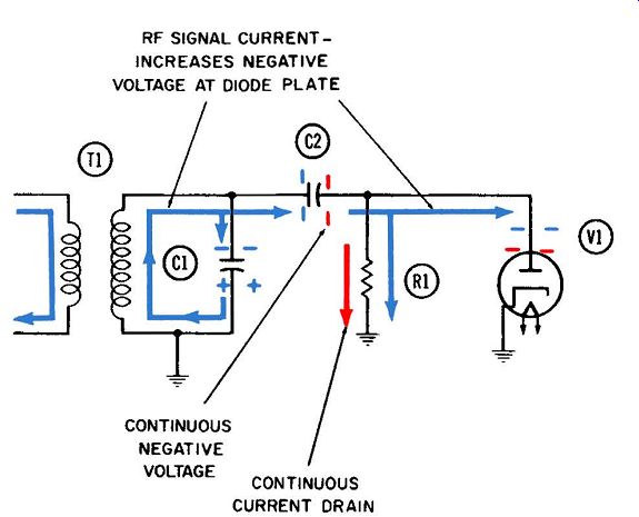
Fig. 4-1. The diode-detector-negative half-cycle.

Fig. 4-2. The diode-detector-positive half-cycle.
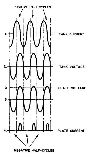
Fig. 4-3. Tank- and plate-current and -voltage waveforms in the diode
detector circuit.
The action of the tank voltage alternately increases and de creases this negative voltage, so that the plate voltage at any instant is the sum of the two voltages. Only when the diode plate is more positive than the cathode will plate current flow.
Let us look more closely at line 3 of Fig. 4-3, which represents the voltage at the diode plate. This voltage is mostly negative and is caused by the accumulation of electrons on the right plate of C2. The size of this negative voltage depends on the strength of the radio-frequency current in the tank; and the latter, of course, depends in part on the strength of the received signal.
If the carrier signal is cut off at the transmitter, as is done during keyed CW communications, the tank current will die out in a relatively few cycles. The diode will then stop conducting, and the negative voltage on the right plate of capacitor C2 will drop to zero as the electrons stored there drain downward through the diode load resistor to ground.
When the carrier signal is resumed at the transmitter, the tank current comes back into being, the diode conducts, and a negative voltage again builds up at the top of the diode load resistor.
Thus, with this circuit, what amounts to a "DC voltage" has been produced; its existence depends on the existence of a carrier signal, and the strength of this voltage will vary in accordance with the amplitude variations (modulation) of the carrier. Hence, we can say the carrier signal has been "demodulated," or "detected."