AMAZON multi-meters discounts AMAZON oscilloscope discounts
PRINTED CIRCUITS have many advantages for the home experimenter.
They can eliminate the need for much drilling and bending of metal chassis. The printed circuit, which is simply a sheet of phenolic plastic covered on one or both sides with copper foil, provides a chassis for mounting components and also provides most of the interconnecting wiring for the parts. Soldering the components into the board not only mounts them physically, but also connects them into the circuit electrically.
Of the various printed-wiring techniques now in use, etching is best suited for home use. An additional method, stripping, is also useful in the home shop, but it is limited to projects where the wiring is simple. Its main advantage is that the only tools required are a hand drill, a center punch, and a heavy-duty hobby knife.
In printed circuits, generally speaking, all components are mounted on one side of the base. This is not a hard-and-fast rule and can be varied to suit individual needs. The components can be mounted directly in small-size holes drilled into the copper strip, or an "island" can be formed which is slightly wider than the strip and an eyelet inserted.
Lightweight soldering irons are a must for printed circuits. They should be about 25 to 50 watts and should be used with a fine low-heat solder. Heavy irons and high-temperature solder may cause blisters which would pull the copper laminate away from the phenolic base.
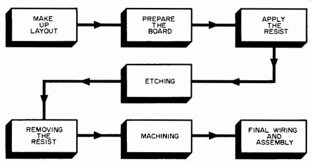
Fig. 56-Basic steps in the preparation of an etched circuit board.
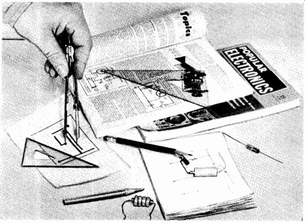
Fig. 57-To make up a printed-circuit layout, start with the schematic diagram
of the project you plan to assemble. Redraw it until you have eliminated all
circuit wiring crossovers.
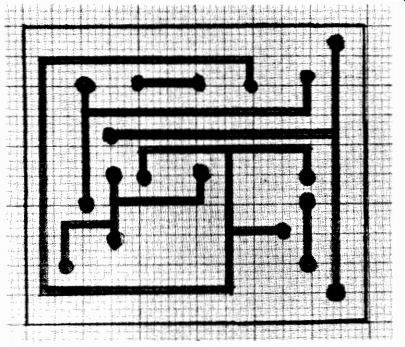
Fig. 58-Typical etched circuit layout.
Laying Out the Circuit
The basic steps in all printed-circuit techniques are similar. First the circuit must be drawn on paper; then the lines are transferred to the copper-foil; finally the foil is removed from the phenolic, leaving only the desired wiring pattern. It is in this last step that the major differences in technique occur.
To make a circuit layout, start with the schematic wiring dia gram of the .project you plan to assemble. Redraw the schematic one or more times, trying to eliminate all circuit wiring crossovers. When you have a tentative circuit, gather the components you plan to use and make a full-size scale drawing of the final circuit.
Locate components where they will serve to bypass conductor crossovers which are not easily eliminated. Individual leads or "wires" should have a thickness of at least 1/3,) inch, with the spacing between adjacent conductors not less than 1/32 inch. Thicker leads can be used if desired, and you may find it easier to work with 1/16-inch- or even 1/8-inch-wide conductors on the first few boards you make up.
Where components are to be mounted or leads attached to the board, draw small circles. Entire patches of foil conductor can be used for shielding, although it is generally best to break up solid areas with diagonal bars. The spacing between adjacent bars may approximate or be slightly greater than the width of the bars. Where 90-degree turns are made, the conductor may follow a smooth curve or make a sharp bend, as preferred. Where eyelets are to be used, plan on holes large enough to accommodate them. Use slightly smaller holes when leads are to be attached directly to the copper foil.
In general, component and wiring leads can be soldered directly to the copper foil for permanent connections, but if the leads may be removed often, plan on using copper or brass eyelets at such points. Space component mounting holes for the actual parts you plan to use. If the components are to be mounted by their leads (resistors, capacitors, and small coils are generally mounted in this fashion), space the mounting holes with the thought of using a gradual bend in the component leads instead of a sharp bend close to the body-sharp bends may cause the leads to break off or may place an undue strain on the component.
You will find that graph paper is useful for making up the scale wiring layout.
A typical printed-circuit board for a wiring layout is illustrated in Fig. 59. This layout has been designed to illustrate important points to remember when making up your own layouts and does not represent a specific circuit.
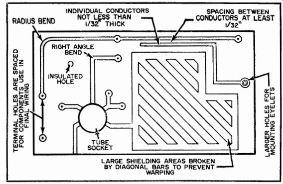
Fig. 59-Typical printed-circuit board.
Upon completing a circuit wiring layout, check and double check for errors. While still in the layout stage, an error may be corrected simply by erasing and redrawing the layout. But once the board is etched, it may be necessary to make up an entirely new board to correct mistakes.
The copper-clad phenolic board and other materials can be purchased individually, or in kits, from radio supply houses. At the beginning, however, it is best to purchase a complete kit of materials. After you have gained a little experience in making up circuit boards, you can purchase individual items in the quantities needed.
Depending on the circuit layout, use either single-sided (single-clad) or double-clad boards. But until you have gained experience, you will find it best to stick to simple layouts and single-clad boards.
Cut a piece of the copper-clad board to fit your circuit layout, using a fine-toothed hacksaw, a jigsaw, or a scroll saw. Cut from the copper side, and back up the thin phenolic board with a piece of hardboard or plywood. Any large holes or cutouts needed (for tube sockets, for example), should be cut at this time. Use a hole saw or fly cutter for cutting large, round holes. Do not use a conventional chassis punch; this may crack the board. Only the large holes and cutouts should be made at this time. Smaller holes can be drilled after the board is etched.
After the board has been cut to size and the rough machine work completed, clean off dirt and tarnish from the copper surface, and roughen it slightly to permit the etchant to get a better "bite" on the foil. Do this by scrubbing the surface with a stiff brush and an abrasive household cleanser. Sprinkle the household cleanser lightly on the foil and scour vigorously with a slightly dampened cloth. With the surface properly prepared, the copper should be bright and shiny and should have many small scratches that are visible when the foil is examined through a small magnifying glass. Rinse and dry the prepared board.
Obtain a few sheets of "pencil" carbon paper from your local stationery store. Cut a piece to fit your circuit board and attach the carbon paper and scale wiring layout to the board with Scotch tape. Make sure the layout cannot shift its position. Finally, using a moderately hard pencil, trace the layout onto the copper foil.
Locate small mounting holes by pricking the copper right through the layout and tracing carbon, using a small center punch or a sharp scribe. In order to avoid cracking the board, use hand pressure or a very light hammer tap when locating these holes. Back up the board with a solid piece of hardboard or wood. Double check your tracing before removing the layout sheet and carbon paper.
After the circuit layout has been transferred to the copper-clad board, the acid "resist" can be applied. For experimental "single-shot" circuits, two types of resist are popular:
(1) ink resist and (2) tape resist.
Ink resist is an asphalt-based, acid-resistant paint or ink. It is sup plied as a part of most printed-circuit kits, and, also, is available from many art supply houses. Apply ink resist to the copper foil using a small ruling pen, a small brush, or a "Speedball" pen. Cover all parts of the wiring layout, because only those parts of the copper foil covered by the ink will remain after etching. Allow the ink to dry.
Ordinary plastic-base Scotch electrical tape makes an excellent tape resist. Narrow strips can be cut from the standard width using a sharp knife or razor blade. Small circles, for terminal connections, can be punched out with a hand paper punch. The tape is applied to the cop per foil to cover the traced wiring paths on the layout pattern, then burnished down in place with a soft hand tool. A good burnishing tool can be made quite easily by rounding the end of a wooden dowel peg.
Double check the circuit board after applying the resist. Compare it to the original layout. If you find you've made an error, correct it. Ink resist can be removed by using a hard (ink) eraser; tape resist is simply peeled off. Reapply the resist to correct the error.
A ferric-chloride solution (FeCl3) is used to etch the board. This is available in either liquid or powdered form. It can be purchased at photoengraving supply houses in liquid form and from some drug stores and chemical supply houses in powdered or lump form. If you use the etchant from a kit, follow the instructions furnished with it.
If you obtain a ferric-chloride solution from a photoengraving supply house, it will be listed as "42 percent ferric-chloride." This solution is rather thick and should be diluted before use. Add plain water in proportions of one-half pint of water to one quart of solution.
If you obtain the ferric chloride in powdered form, dissolve it in a Pyrex glass or an enameled container. The proper ratio is approximately 3 ounces of ferric chloride to 6 ounces of water. The dissolving action is exothermic-that is, heat is evolved as the ferric chloride goes into solution-so don't worry if the solution heats up slightly.
Use care when working with the etchant. It can stain clothing.
Although it is not especially dangerous, the ferric-chloride solution is "bitev" and may irritate sensitive skin. Wear rubber gloves when working with it.
The actual etching is carried out in a small, flat tray that is similar to those used by photographers. A shallow Pyrex cooking dish makes an excellent tray. Either "hot" or "cold" etching can be employed. The hot etching technique is slightly faster than cold etching. For the hot etching method, obtain a small hotplate and either a Pyrex dish or tray or an enameled metal tray. If you use the cold method, a shallow plastic box or tray can serve as the etching container.
To etch the circuit board by means of the "hot" method, pour a sufficient amount of the etchant into the tray to cover the circuit board to a depth of about 1/4 to 3/8 inch. The actual amount of etchant used is not critical as long as the board is completely covered. If in doubt, always use a larger quantity. Place the tray on the hot plate and turn on the heat. Drop the circuit board gently into the etchant, taking care not to splash the solution. Copper side should be up. Move the board around from time to time during the etching process, using a plastic or glass rod or a pair of plastic tongs.
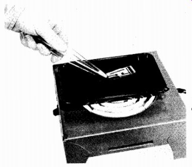
Fig. 60--Hot etching of printed circuit board.
In general, as the temperature of the etchant is raised up to the boiling point, the speed of the etching action increases. If it is too hot, however, excessive water evaporation will take place, concentrating the solution and slowing the etching process. An ideal etching temperature is between 90° and 130° F. After considerable etching using the hot method, a little water can be added to the solution to replace the water lost through evaporation. An average circuit board can be etched with the hot method in about two to five minutes, depending on the condition of the etchant, the amount of exposed copper, and the actual etching temperature.
To etch the circuit board by the cold method, pour about 1 inch of etchant into the tray. Drop the board gently into the tray, copper side up. Rock the tray slightly during the etching process so that the etchant moves back and forth across the surface of the board. The average etching time is ten to twenty minutes.
Regardless of the method used, continue the etching process until all exposed copper is removed, leaving only the copper foil protected by the resist.
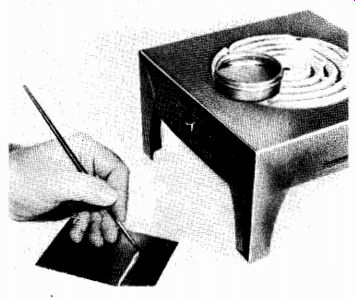
Fig. 61
After the etching has been completed, the etchant can be returned to a tightly sealed storage jar or bottle and the circuit board thoroughly rinsed under clear running water. Allow the board to dry.
After thorough rinsing and drying, the resist should be removed from the board, leaving the copper-foil "printed" circuit.
Ink resist can be removed by rubbing with steel wool, and a final cleaning can be made using a soft cloth dampened slightly with a general-purpose solvent such as General Cement No. 31-16 x. Tape resist is simply peeled off.
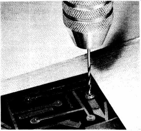
Fig. 62--Drilling component mounting holes in printed-circuit board.
Component mounting and eyelet mounting holes are then drilled in the etched board at the points required. Normally, a size No. 52 drill is used, but a slightly smaller or larger drill may be employed in some cases. Use a solid backing for the board during drilling to avoid cracking the phenolic. After the drilling has been completed, mount eyelets (brass or copper) in appropriate holes. Eyelets are usually mounted wherever connections are likely to be removed and replaced frequently.
Where permanent connections are to be made, eyelets are not necessary.
Resistors, capacitors, coils, and similar components are mounted by passing their leads through appropriate holes in the etched circuit board. The customary practice is to mount these components on the back (non-etched) side of the board. When mounted in this position, lead tension tends to hold the foil in place instead of pulling it away from the base. Leave the component leads full length. After passing the leads through the holes and pressing the component tightly against the board, the leads are bent slightly to one side, holding the components in position through natural tension. Circuit crossovers, where necessary, can be made with short lengths of ordinary hookup wire that has been stripped at both ends.
When all leads have been soldered in place, projecting wires can be cut off close to the circuit board using a pair of diagonal cutters. As a final touch, the completed circuit can be given one or two coats of silicone resin, either sprayed on from a pressure-type can or applied with a small brush. This insulates and protects the completed circuit and reduces the chances of arcing between adjacent conductors under conditions of high humidity. Either type of silicone resin is available from General Cement Company as Type 14-6 (spray) or Type 14-2 (liquid).
Cutting Corners
The most time-consuming steps in the preparation of an etched circuit are laying out the circuit and applying the resist. Here it is best to use simplified techniques to accomplish your objective.
You can acquire skill in designing circuit layouts by making up practice designs based on the schematic diagrams of various construction projects. It is not necessary to carry the circuit through to final etching and assembly to make this practice of value. You should learn to visualize a circuit in terms of two-dimensional wiring.
Once you have acquired skill in layout, you will find that you can eliminate the initial step entirely and design your layout as you apply the resist to the copper-clad board. Then you can simplify the latter step by using a type of resist that is easy to apply. However, be sure to clean the board before applying the resist.
The conventional resist, asphalt-based ink, is messy to use; it dries rapidly and becomes thick, making it difficult to apply. Tape resist, although cleaner to use, is tedious to apply; the tape must be burnished against the copper-clad board to ensure good adhesion. If care isn't taken here, the etchant will eat under the tape and ruin the circuit board.
Fortunately, there are other resists suitable for etched circuit work that do not have such disadvantages. Paraffin wax is a resist used for centuries in the acid etching of metals and glass.
There is a definite technique to applying a paraffin wax resist to a circuit board.
First, melt the wax in a small metal container. Make sure that all the wax is thoroughly melted (good-quality wax will look like water when liquid), but don't allow it to overheat or to smoke.
It is very important to preheat the copper-clad board. If the board is too cold, the applied wax will freeze on its surface. When the board is preheated, the wax will spread and flow over the surface.
The wax is applied to the board with a fine brush (see Fig. 62).
Simply paint the pattern you wish directly on the board.
A paraffin wax resist is suitable for all types of etched circuit boards. However, you must use a cold etching process when you use a wax resist; hot etchant will melt the wax and ruin your circuit board.
Stripping
A simplified technique that will eliminate the etching process can be used where the circuit is not complicated. With a heavy-duty hobby knife, cut away the unnecessary copper foil. These pieces can then be stripped off by hand, leaving only the desired wiring pattern.
This method consists first of planning the layout on a piece of paper. Draw out the design, employing the actual components to be used to help provide physical dimensions. After the design is considered satisfactory, transfer it to a piece of 1/16-inch copper laminate by using a center punch or scribe. With a sharp model knife, cut the pattern into the copper, then peel off the unwanted portions.
Almost any circuit can be put on a printed-circuit card. Here is a step-by-step explanation of how to make a printed circuit, using a simple radio control receiver as an example. (The original circuit and the finished circuit board are shown in Fig. 63.) Gather all the components called for in the circuit. Plan on making the copper lines wider than actually necessary-%2 inch to 1/5 inch should be ample. (Finer lines and extreme miniaturization may be at tempted later.) So that the tube may be removed, use miniature tube sockets for subminiature tube leads. Use eyelets if the tube is to be soldered onto the base.
With the parts, paper, pencil, and rule, juggle the components around, using the schematic to determine where to place each part.
Using many sheets of paper in this step of the process will produce a much neater unit.
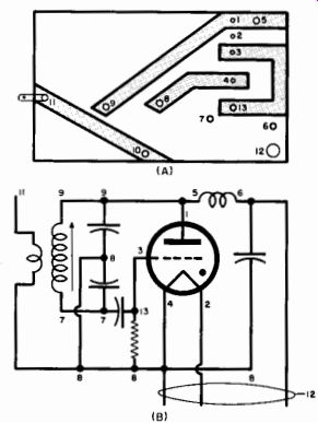
Fig. 63-Original radio control receiver circuit (top) and stripped circuit
board (bottom). Numbers indicate corresponding points.
When the layout is satisfactory, double check to make sure the wires correspond to the schematic.
Cut the copper laminate to the size required for the base. With a center punch, scribe, or any sharp-pointed tool, transfer the paper pat tern to the copper side of the laminate. Connect the lines and draw a pencil pattern of the strips desired. With a sharp model knife, cut these lines just heavily enough to penetrate the copper (see Fig. 64). Practice on some scraps will help you to determine the amount of pressure required.
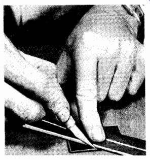
Fig. 64
After all lines have been scored, use the knife to cut between the copper and the base and slowly peel off the unwanted copper (see Fig. 65). Take this step slowly; too hasty a pull may yank loose some of the copper wanted for wiring.
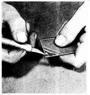
Fig. 65
After the card has been completely stripped, use steel wool to smooth off any rough edges on the lines (see Fig. 66). Drill the holes required by the layout, using a sharp drill.
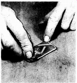
Fig. 66
With a lightweight soldering iron, mount the components, then snip off the excess leads. If the layout is correct and all solder joints have been made properly, the set should be ready to go. That's all there is to it!