AMAZON multi-meters discounts AMAZON oscilloscope discounts
LEARNING OBJECTIVES:
Upon completion of this Section on printed circuit board materials, the student should be able to:
1. Know the classification of printed circuit boards.
2. Be familiar with the characteristics of printed circuit cable.
3. Be familiar with the various grades of rigid printed circuit laminates and their characteristics.
4. Understand the properties of copper foil on rigid printed circuit boards.
5. Select the appropriate grade of printed circuit laminate and copper foil thickness to satisfy the specifications for a variety of applications.
0. INTRODUCTION
With the advent of the transistor and the more recent heavy reliance on integrated circuits, electronic packaging and wiring problems have been compounded. No longer can the technician rely solely on hand-wiring methods; now designs must be oriented toward more extensive use of printed circuitry. Many modern electronic systems would be virtually impossible to package without incorporating printed circuits into their design.
Printed circuits are metal foil conducting patterns, usually copper, bonded to a substrate (insulating base material) for support. The metal pattern serves as the connecting medium for the electrical components that are assembled on the opposite side of the board. Component leads are fed into holes that are drilled or punched through the base material and foil. These leads are soldered to the conducting pattern to form the complete printed circuit.
The advantages of printed circuits over conventional wiring methods are that they (1) adapt easily to miniaturization and modular design, (2) provide for uniformity in production, (3) lower costs, (4) virtually eliminate wiring error, and (5) minimize assembly and inspection time. Printed circuit techniques lend themselves readily to mass production, resulting in a highly reliable package. Although the format of this text is focused on prototype construction, it must be assumed that eventually the package will be released for production. Consequently, the technician should design the package with an eye toward this end by selecting materials and configurations that will reduce construction problems.
To completely understand the sequential process involved in printed circuit board design and fabrication, the next 13 Sections will be devoted exclusively to these topics. This Section discusses the initial step in printed circuit construction—the selection of the most appropriate type of printed circuit board material. Topics discussed are classification of printed circuit boards, insulating base materials, conductive foils, bonding, and tabulated information of board characteristics to aid the technician in selection.
1. CLASSIFICATION OF PRINTED CIRCUIT BOARDS
Printed circuits are designed as either rigid and are further classified into s -sided doubled-sided or multilayer conductors. Regardless of the type, all printed circuit boards are formed with an insulating base material on which a conducting foil is either chemically or mechanically bonded. When processed, the printed circuit board provides both an electrical wiring path and a mechanical support for the components.
Rigid printed circuit boards of the single-sided type are the most frequently used, finding extensive application in relatively uncomplicated circuitry. Figure 10.1a shows a rigid single-sided blank before processing. The completed conductor pattern ready for component mounting is shown in FIG. 1b.
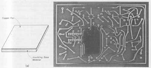
FIG. 1 Rigid single-sided printed circuit boards: (a) copper-clad printed
circuit blank; (b) processed single-sided printed circuit conductor pattern.
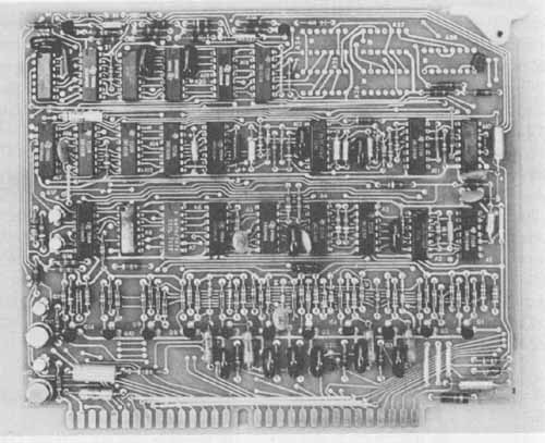
FIG. 2 Assembled double-sided rigid printed circuit board.
Rigid printed circuit boards of the double-sided type consist of conducting foil bonded to both sides of the insulating base. This type of board is employed when circuit complexities make it difficult or impossible to develop practical wiring layouts on one side only. Double-sided boards also reduce the size of a comparable circuit constructed on a single-sided board, since components are mounted on both sides. Figure 2 shows an assembled double-sided board. Interconnections among the conductive patterns on both sides of the board are typically accomplished by plated-through holes, which is a manufacturing process discussed in Section 16. With the use of these interconnections, wires or component leads can be soldered between the foil patterns on opposite sides of the base materials.
Multilayer rigid printed circuit materials were developed to satisfy the needs of the more recent state of the art, which demands extremely complex wiring layouts in a relatively small space. Multilayer board material selection as well as fabrication are discussed in detail in Section 20.
Flexible printed cables consist of conductors laminated between layers of insulation and exposed for soldering only at the terminal points, as shown in FIG. 3. Flexible printed cables are used in a manner similar to ordinary cable but are extremely flexible. In addition, the flat configuration of these circuits make them desirable for system interconnections where a round cable may prove to be too cumbersome. Teflon, polymide, polyester, polyvinyls, polypropylene, and polyethylene are typical insulating materials used in flexible printed cables. TABLE 1 shows a comparison of the various characteristics for common insulations. Since various methods and adhesives are used for the internal bond of these laminates, no one method of insulation removal will suffice for all types of these cables. The insulation is usually stripped by friction wheel strippers, knife-edge strippers, chemical dipping, or melting by a concentration of hot air. Because flexible printed cables have a large flat conducting area, they can handle larger currents than conventional wire cable. TABLE 2 shows the approximate current capacities and derating values when a multiple number of conductors are laminated within a common cable.
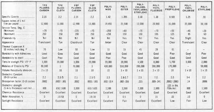
TABLE 1 Insulation Characteristics for Flexible Printed Cables.
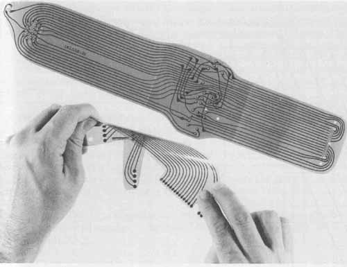
FIG. 3 Flexible printed circuit cables. Courtesy of DuPont Company.
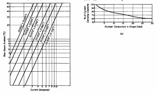
TABLE 2 Conductor Temperature Rise and Current Derating for Flat Cables:
(1) Rise in Temperature above Ambient as a Function of Current; (b) Approximate
Derating Curve for Flat Cable
2. INSULATING BASE MATERIALS FOR PRINTED CIRCUIT BOARDS
Printed circuit boards of the rigid variety will be discussed exclusively in the remaining sections of this text since they are by far the most common. The insulating or resin material for these boards is either a thermosetting plastic or a high-temperature that provides the support for the conductor pattern and components. The discussions will be limited to the thermosetting plastics, since they are used almost exclusively in rigid boards.
Base materials for printed circuit boards are laminates containing a rein force such as paper, glass, or fabrics, including cotton cloth, asbestos, nylon cloth, and glass cloth. These laminates are formed under pressure and heat. The thermosetting plastic resins common to the manufacture of printed circuit boards are phenolic, epoxy, melamine, silicone, and Teflon. Silicon-glass is mechanically inferior and more expensive than either phenolic, epoxy, or melamine resin boards. Teflon is used primarily for microwave applications and is approximately fifteen times more expensive than phenolic and at least five times as costly as the epoxy and melamine resin types. The phenolic types are less expensive than the epoxy resins and for many applications are both electrically and mechanically suitable. In general, the epoxy types possess superior electrical and mechanical characteristics than phenolic or melamine. In most cases, the reliability of a particular type of board will by far outweigh the cost factor.
To aid the technician in selecting the most suitable base material for a specific application, there follows a description of some of the electrical, mechanical, and chemical qualities of the more common base materials. The classifications are in accordance with NEMA (National Electrical Manufacturers Association) standards. These standards designate phenolic resin printed circuit boards as either X, XX, or XXX, which represent the amount of resin present, the amount increasing with the number of X’s. In general, the more resin content, the more improved are the electrical and mechanical characteristics of the board. A P suffix together with the X designation denotes that the phenolic is capable of being punched but only at elevated temperatures, where a PC suffix indicates cold-punch qualities.
Grade XX. This grade of paper-base phenolic possesses fair electrical characteristics and good mechanical properties. It machines well but is not recommended for punching. It little abrasive action to drills and, as a result, does not dull these bits easily. This grade is used by many manufacturers as a reference for determining the costs of other laminate types. For example, if the price index of nylon cloth phenolic is 3.5, this indicates that its cost is that much more than grade XX, which has a cost index of 1 (see TABLE 4).
Grade XXP. This type is similar in electrical and mechanical p to grade XX and it can be punched at increased temperatures of between 200 and 250°F (93 to 121°C).
Grade XXX. This material possesses some improved electrical and mechanical properties over the XX type and is recommended for use at radio frequencies. It is available in a self-extinguishing form, meaning that it will not support combustion if ignited. This grade possesses fair dimensional stability (i.e., it maintains its size within close tolerances under environmental changes such as temperature and moisture).
Grade XXXP. This grade is recommended for most general-purpose applications and is similar to grade XXX, but possesses an additional advantage in that it can be punched at elevated temperatures. Frequencies up to 10 MHz are permitted with this grade.
Grade XXXPC. This is similar in electrical and mechanical properties to grade XXXP board and has higher insulation resistance lower water absorption. These qualities make this type of board particularly useful for high humidity applications. In addition, this material can be punched at temperatures of 70 to 120°F (21 to 49°C). For these reasons, XXXPC printed circuit boards are widely preferred over grades XX and XXP. However, when punching and moisture are not considerations, grade XXXP is generally selected.
Grade G-5. This is a melamine base material with excellent electrical and mechanical properties. It is the least expensive glass cloth base but it is one of the most abrasive grades and, as a result, is very seldom used for general-purpose printed circuit applications.
Grade G-10. Manufactured with a glass-cloth reinforcement and epoxy resin, this grade possesses superior electrical and mechanical properties when compared to phenolic boards. Because of its high flexibility, low dielectric losses and moisture absorption, and high bond strength between the base and the conducting foil, this laminate is widely used and is recommended for frequencies up to 40 MHz.
Grade G-11. Also employing a glass-cloth reinforcement with epoxy resin, this grade is similar in characteristics to grade G-10 but is more flexible at higher temperatures. In addition, it is more resistant to acids, alkali, and heat than G-10, but is more difficult to machine. The cost of both of these grades is the same.
Grade FR-3. This grade is designed for optimum balance of electrical and mechanical properties and is manufactured with paper reinforcement impregnated with epoxy resin. It is considered superior to grade XXXPC because of its higher arc resistance, lower moisture absorption, and improved dimensional stability qualities. It is used almost exclusively as a self-extinguishing type in the higher frequency ranges, up to 10 mhz.
Grade FR-4. This grade is identical to grade G-10 with the addition of flame retardants. For this reason, it is currently the type most often specified for applications in minicomputers, CB radios, and military and aerospace instrumentation equipment.
The information presented for these various types and grades of laminates is included with additional information in Tables 3a, 3b, 4, and 5. These tables provide for a complete comparison of a wider range of electrical, mechanical, and chemical properties of the described grades, in addition to many other base materials and their properties. All of these properties should be evaluated when selecting the most suitable base material for a particular application.
Single- and double-sided copper-clad laminates are available in sheets that range from 26 to 36 inches wide by 36 to 48 inches long. Smaller, precut dimensions are also available at extra cost. The thicknesses of the laminates, including the copper foil, range from to inch in increments of inch.
A characteristic of all printed circuit boards is their tendency to warp and twist. These conditions are the result of the two dissimilar materials (base and copper foil) bonded together to form the laminate. After etching, however, the boards will significantly straighten out because of the large amount of copper loss. Warp and twist describe the deviation of the board from a straight line fixed by two points at the extremities of the board. To determine the degree of warp, this line is taken along the longest edge. Twist is evaluated along a diagonal line between opposite corners of the board. These values of warp and twist are expressed in percentage of board or diagonal length, with the thinner boards tending to warp more than the thicker ones. Deviations range from approximately 12% for a thickness of to 5% for a i-inch thickness. Double-sided boards reduce these values by at least a factor of 2. These deviations of the boards become important considerations when designing for plug-in-type circuits, wherein only extremely small amounts of warp or twist can be tolerated.
3. CONDUCTING FOIL
Copper is the principal type of foil used in the manufacture of printed circuits. For special applications, nonstandard materials such as aluminum, steel silver, and tin foils are used. Copper foil has the advantages of high conductivity, excellent soldering characteristics, low cost, and ready availability in a variety of widths. The copper used for printed circuits is at least 99.5% pure in order to maintain its high-conductivity properties.
The manufacturers of copper foil for printed circuit applications employ two basic production methods. These methods are termed rolled foil and electro-deposited foil. Rolled foil is formed from refined blocks of pure copper. The foil thus produced is largely free of pinholes and imperfections and has a smooth surface on both sides. Made in widths not exceeding 24 inches and thicknesses less than 0.00 1 inch, this rolled film has excellent tensile-strength properties. Because of its smooth surfaces, however, rolled foil requires special bonding treatments to enhance the wetting between the adhesive and the foil and to remove contaminants.
Electro-plated foil used almost exclusively in the manufacture of printed circuit boards, is produced by the plating of the film from solutions of copper sulfate or copper cyanide on a revolving stainless steel drum from which the foil is continuously stripped. The inner surface of the resulting film exhibits a smooth finish whereas the outer surface is coarse, thereby promoting improved bonding with the increase of surface area. The thickness of the foil is controlled by the solution concentration and the electrical and mechanical parameters of the plating process. Thicknesses of less than 0.00 1 inch and widths in excess of 5 feet are obtainable by this method.
Foil thickness, regardless of the manufacturing process, are specified for printed circuit boards in ounces of foil per square foot. Foils of 1 ounce per square foot have a thickness of 0.0014 inch, whereas 2- arid 3 ounce foils have thicknesses of 0.0028 and 0.0042 inch, respectively. Other available thicknesses are shown in TABLE 6, which gives film thickness with the thickness tolerance.
The selection of a thickness of copper for a particular circuit application is determined principally by the amount of current that it must be able to handle. This current-carrying capability depends primarily upon the thickness and width of the conductor path, in addition to the temperature. Owing to the larger radiating conductor surface area, the current capacities of printed circuit boards can easily approach 50 amperes. TABLE 7 shows the maximum cur rent capacities for several conductor width and foil thicknesses to aid in the proper weight selection.
4. BONDING
The manufactures of printed circuit boards choose the proper adhesives to bond the conducting foil to a particular base material in order to produce copper-clad laminates that will suit the needs of a variety of applications. The characteristics of bond strength hot solder resistance, and chemical resistance, as listed in the tables in Sec. 3, largely depend on the particular adhesive used by the manufacturer for bonding and therefore will influence the technician’s choice of board. Of these characteristics, bond strength is one of the most important. This affects the reliability of a printed circuit board. If the foil should lift from the base during manufacture or in service, repair is virtually impossible. The bond must withstand the stresses involved in processing, fabricating, and servicing the printed circuit. These stresses include chemical attack from etching solutions; physical forces introduced through shearing, bending, twisting, shock, and vibration; and thermal shock during the solder in process. When shearing large sheets of single-sided copper-clad laminate into smaller blanks, the foil side should be facing upward with the insulating base material against the shear table. By cutting through the foil side first, there is less tendency of tearing the foil away from the edge of the blank. In addition, care must be exercised that the shear blade be allowed to return slowly to its normal position as it passes the newly cut edge of the board. If the blade were allowed to spring back quickly, it might snap the edge of the board just enough to crack the base material and upset the bond along that edge.
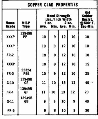
TABLE 5 Copper-clad Properties
TABLE 6 Copper Foil Thickness Tolerances
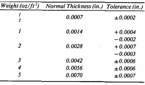
TABLE 7 Maximum Recommended Current-Carrying Capacity for Various Conductor
Widths and Thicknesses
The two most common types of adhesives used in printed circuit bonding are vinyl-modified phenolics and modified epoxys. Although both adhesives display excellent bonding qualities; the epoxy resins are superior in this respect. The manufacturing process of bonding involves the application of a uniform thickness of adhesive on the foil, after which it is forced-air-dried and laminated to the base material in a press. Once the adhesive has cured, the excess foil is trimmed around the edges of the board. Finally, the foil is cleaned to remove all films and oxides resulting from the manufacturing process.
5. BOARD SELECTION
Selecting the most appropriate printed circuit board grade for a particular application depends primarily on the mechanical and electrical requirements of the circuit. The information contained in Tables 3a, 3b, 4, and 5 will dictate which grade of board is most suitable for a specific application. An evaluation of the various board characteristics will be made with reference to selecting the most appropriate grade of base material for the amplifier’s printed circuits. This example will serve as a guide to illustrate the important factors that need to be considered for proper board selection.
Example: A printed circuit board grade is to be selected to meet the amplifier circuit’s requirements as follows:
Type of construction: prototype
Maximum continuous current: 1.6 amperes
Maximum voltage: 36 volts
Frequency: audio range (maximum 20 kHz)
Board mounting: corner securing by machine screws to metal chassis
Hardware mounting: swaged terminals and machine screws
Machine operations: drilling and shearing only
Soldering: hand
Grades of printed circuit boards containing silicone or Teflon resins are not considered because of their higher cost and high-frequency characteristics that are far beyond the requirements of the amplifier. Melamine resin boards are also not considered because of their extremely abrasive characteristics, which make them difficult to drill.
One important consideration for comparison and selection is hot solder resistance. This characteristic expresses thermal bond strength as a function of time and temperature. Since the boards will be hand-soldered, it is difficult to accurately control soldering time and temperature. Therefore, a board grade with a moderate to high value of hot solder resistance should be selected. TABLE 5 compares some common boards. The FR and the G grades are found to be superior to the phenolic grades listed.
Bond strength also needs to be considered in terms of the mechanical stresses that result from the fabrication of the board. Tables 10.3a, 10.3b, 10.4, and 10.5 show that the epoxy-glass resins have a higher bond strength than all the other grades with FR-4 and G-10 having high comparable values of bond strength.
Warp and twist are of no great concern, since all the boards in the amplifier circuit are to be secured to the chassis element with machine screws and nuts.
The machinability of the board is another important mechanical consideration. As shown in TABLE 4, the phenolics can be drilled easier than the epoxy-glass types. Finally, the base material’s mechanical strength must be taken into account. Mechanical strength and machinability are inversely related. The epoxy glass is stronger than the phenolics. Since mounting holes will be formed in the corners of each board and terminals will be swaged to serve as circuit interconnections, fracturing of the base material is a necessary consideration. Although the machining of the glass-base epoxy materials is more difficult than that of the phenolics, this characteristic is not as significant as mechanical strength of the laminate in the selection process. Machinability refers to the ease or difficulty of drilling or punching and the abrasive action of the material, which affect the selection of tools and methods of machining. Because no punching or machining other than drilling will be performed on any of the boards used in the amplifier, the mechanical superiority of glass-base epoxy outweighs the small difference in machinability characteristics.
In considering the electrical characteristics, as shown in Tables 3a, 3b, 4, and .5 all the board materials listed for the amplifier circuits have parameters which are in excess of those required. The parameters if dielectric constants, and dissipation factor are the most important for high frequency applications. Therefore, since the amplifier will operate in the low-frequency (audio) range, these parameters need not be considered here. For dc to low-frequency applications, the parameters that must be considered are arc and tracking resistance, insulation resistance, and dielectric breakdown voltage.
Arc resistance is the ability of a base material to prevent undesired conducting paths created by an arc among portions of the existing conductor pattern. Tracking resistance describes the formation of undesired conductor paths through the insulating material. These characteristics need not be considered at low power and low voltage applications, such as the 36 volts maximum of the amplifier.
Insulation resistance, expressed in megohms, is the measure of the total leakage resistance among adjacent conductors. Because of the extremely high ohmic values, as listed in TABLE 5, this parameter does not become a consideration for this application.
Dielectric breakdown voltage is a function of the spacing among conductors and, as such, need not be considered here for purposes of board material selection. This property will be discussed under conductor spacing in Section 11.
Based on the mechanical and electrical requirements of the amplifier circuit and comparing the properties of the various laminates in the tables provided, grades XXXP, FR-4, G-10, and G-11 appear to be the best choices to obtain a realistic compromise. In our selection process, we first eliminate grades XXXP and G-11 because their bond strength and machinability values are lower. Also, grade XXXP is not as strong mechanically as FR-4 and G-10.
For our amplifier circuit, either grade FR-4 or G-10 is suitable since they have comparable properties for this application. However, even though it is of no concern to our amplifier circuit, grade FR-4 does have one additional advantage over grade G-10 in that it has a much higher flame retardancy value, as seen in TABLE 4. Since the cost of these two grades is about the same, we will select grade FR-4 for our amplifier circuit.
One final consideration that also influences the selection of the FR or G series over the phenolic types is the ease of tracing circuits on the completed printed circuit board. As shown in TABLE 3a, the phenolics are available in opaque natural brown, or black colors. The brown color is used almost exclusively with printed circuit boards. The type FR or G grades are generally trans lucent with a green tint. This translucent characteristic is extremely helpful in inspecting circuits. It is difficult to compare component and conductor pat terns with a schematic diagram when the base material is opaque. By holding the translucent board up to a strong light, the relationship among components and conductor pattern is easily seen.
With the base material selected, the final step is the choice of the most suitable base thickness and copper foil weight. As mentioned previously, warp and twist present no problem in this amplifier package. Since all boards will be firmly secured to the chassis element, no other mechanical parameters need to be considered. For these reasons, -inch base material will be used. For the smaller boards, i-inch material may be used; but for the sake of consistency and to avoid board fracture, especially around swaged terminals and mounting holes, all boards in this package will be inch.
In selecting the foil thickness, the major consideration is the amount of current that the circuit is expected to handle. The maximum circuit current is 1.6 amperes. From TABLE 7, for a typical conductor width of 0.030 inch, the maximum current capacity for 1-ounce cop foil is approximately 1.9 amperes This standard 1 ounce foil, which will easily meet the circuit current demands, is therefore selected.
In summary, the solution to the problem of board selection for the amplifier package is -inch 1-ounce FR4 single-sided copper-laminated printed circuit board.
The printed circuit board having been selected, the technician must next prepare the necessary drawings and artwork for transforming the schematic diagrams of the various circuits into conductor patterns that will be later processed. In the following Section we develop the techniques for producing printed circuit conductor pattern artwork.
EXERCISES
A. Questions
1 List the advantages of printed circuit boards over conventional wiring methods.
2 What does the abbreviation NEMA represent?
3 Describe the meaning of NEMA suffixes X, P, and C.
4 What is the temperature rise of a 0.005- by 0.062-inch conductor if the current through it is 4 amperes?
5 Using TABLE 3a, select the laminate that provides the optimum balance of mechanical and electrical properties.
6 Referring to TABLE 4, match the grades of insulation independently in terms of the least and most desirable characteristics of cost, machinability, punching quality, water absorption, bond strength, and arc resistance.
7 Using TABLE 7, select the minimum conductor width for 1-, 2-, and 3-ounce copper foil if the maximum dc current rating is to be 2.5 amperes.
8 What is the advantage of using flexible printed cables as compared to round cables?
9 What causes pc boards to warp and twist?
10 Referring to the tables provided in this Section, determine the optimum pc insulating material and minimum conductor thickness and width to meet the following requirements: 1-ampere dc current, a frequency of 20 kHz, drilling and shearing operations only, wire-wrap terminals, and finger-type connectors for lead and conductor path connections.
B. True or False
Circle T if the statement is true, or F if any part of the statement is false.
1 Grade FR-4 pc boards have a greater flame retardancy than grades G-10 or G-11. T F
2 As the copper foil weight in ounces per square foot doubles, the foil thickness will also double. T F
3 The more Xs in NEMA standards for designating phenolic resin in pc boards, the higher the resin content and the better the punching quality. T F
4 Foil thicknesses are designated in ounces per square inch. T F
5 When shearing blanks of single-sided pc boards, the copper foil side should be facing upward. T F
6 The current-carrying capacity of a printed circuit conductor path is dependent on temperature, foil thickness, and path width. T F
7 For any given foil thickness, as path width increases, current-capacity decreases. T F
8 Mechanical strength and machinability of pc boards are inversely related. T F
9 A PC suffix on the NEMA standards indicates that the pc board may be punched at elevated temperatures. T F
C. Multiple Choice
Circle the correct answer for each statement.
1 Printed circuit board material manufactured from (epoxy, phenolics) offers little abrasive action during drilling.
2 Printed circuit board material used for microwave applications uses a base material made from (Teflon, epoxy).
3 The principal foil material used in the manufacture of pc boards is (aluminum, copper).
4 A copper fo having a thickness designation 2 oz/ft.^2 has a thickness of (0.0014, 0.0028) inch.
5 The maximum recommended current-carrying capacity of a pc board conductor made from -oz/ft copper foil with a width of 0.050 inch is (1.5, 2.5) amperes.
6 The copper used to manufacture the foil on pc boards must be at least (80%, 99.6%) pure.
7 The most commonly used pc board is the (flexible, rigid) type.
D. Matching Columns
Match each item in column A to the most appropriate item in column B.
COLUMN A | COLUMN B
1. XXXPC 2. Double-sided 3. 99.5% 4. G-10 5. Multilayer PCB 6. 1 oz/ft.^2 7. Flexible PCB 8. FR-4 |
a. Copper purity b. Friction wheel stripper c. Epoxy resin d. 0.0014inch e. Two foil layers f. Cold-punching quality g. Flame retardant h. Four foil layers |