AMAZON multi-meters discounts AMAZON oscilloscope discounts
LEARNING OBJECTIVES:
Upon completion of this Section on artwork design and layout for single-sided printed circuit boards, the student should be able to:
1. Select the appropriate grid system for layout.
2. Prepare the grid and polyester sheet overlay to begin a component and conductor pattern drawing.
3. Be familiar with the criteria for proper layouts.
4. Use layout templates and precut component outlines to develop component layouts.
5. Lay out components in the allotted space so that they are balanced, uniformly distributed, and routable.
6. Be familiar with component layout for automatic insertion applications.
7. Correctly route conductor paths on the layout drawing.
8. Be familiar with the available layout tapes and conductor pattern shapes for artwork masters.
9. Prepare a pad master.
10. Select the appropriate-size conductor width and spacing for artwork masters.
11. Know the acceptable taped pattern configurations.
12. Properly tape and complete an artwork master.
13. Prepare solder and marking mask artworks for silk-screen applications.
14. Be familiar with the design of pc boards using CAD systems.
0. INTRODUCTION
After the most suitable type of printed circuit board has been selected, the next phase in the fabrication of a printed circuit is the design of the conductor pat tern artwork master. A properly designed and constructed master will become a precision instrument for faithfully reproducing the foil configuration in processing the printed circuit board. The artwork constructed must not only accurately form the circuit’s electrical connections but must also provide for the space required for placing the components on the board.
There are several methods of producing quality artwork. However, the use of commercially available precut tapes is one of the more popular techniques. Included for discussion in this Section will be (1) selection of a proper grid system, (2) reduction requirements, (3) development of component and conductor pattern layout drawings, (4) master artwork preparation and tolerances, and (5) solder and marking masks. In addition, the use of CAD systems in designing pc boards is presented.
1. GRID SYSTEMS
To facilitate the placement of components, in addition to providing the proper spacing among the intended conductor paths, some type of uniform spacing system must be used. For most printed artwork applications, grid systems having grid spacings 0.050, 0.10, 0.125 inch are generally used. Grid systems are uniform patterns or arrangements of horizontal and vertical lines that aid in simplifying printed circuit board layout. The thickness of the grid lines is approximately 0.003 inch. Depending on the system selected, every second, fourth, fifth, eighth, or tenth line is accented to a thickness of approximately 0.006 inch. These accent lines aid in laying off dimensions and establishing a tabulated coordinate system to identify specific component or hole positions at the intersections of particular horizontal and vertical lines. Selecting the most suitable grid system depends on factors such as (1) scale reduction, (2) required tolerances, and (3) capacity of the reducing equipment.
Whenever possible, artwork masters should be made four times larger than the actual size of the board pattern (4: 1 scale) to maintain reasonable tolerances. This scale is preferable since any error in component positioning or tape placement made on the master will be reduced by a factor of 4 on the processed board. Another advantage of the 4: 1 scale over smaller available scales is that, from a practical standpoint, this larger size facilitates handling. Al though tapes, device outlines, and other layout materials are available for 4: 1, 2: 1 and 1: 1 scales, the artwork should not be smaller than 2: 1 if reasonable tolerances are to be met. If the photographic processing equipment will not make 4 : 1 reductions or accept a 4: 1 enlargement of a printed circuit design, the technician is forced into using a 2: 1 scale artwork layout. If no reduction equipment is available, only 1: 1 scale artworks can be made. Under these conditions, the technician must exercise extreme care in placing the tapes to realize even a most marginally acceptable board.
Artwork prepared for 4 : 1 reductions on 0.125-inch grid systems are common whereas a 0. 100-inch system is used for close tolerance work. For 2 : 1 reductions, 0.100-inch systems are standard, with 0.050-inch grids used for the closest tolerances. Artwork for a 1 : 1 scale requires a 0.050-inch grid system as a minimum.
One grid system that yields excellent results consists of 0.005-inch-thick filmed translucent polyester (Mylar) lined with black rectangular coordinates. Sheet polyester is preferred since a high degree of dimensional stability, in the order of 0.002 inch in 48 inches, can be maintained. For this reason, commercial artwork makes use of polyester film grid systems almost exclusively. When dimensional accuracy as provided by the polyester system is not required, simple quadruled paper, with intercepts of 0.100 or 0.050 inch, can be used with satisfactory results. Depending on the application and tolerances required, it may be acceptable to sacrifice the high degree of dimensional stability obtain able from a pre-established grid system on polyester to that of simple ruled paper. A sizable saving in cost would be realized by the latter selection.
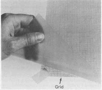
FIG. 1 Overlay method used for artwork master construction.
The polyester sheets must be handled carefully to keep these materials in a workable state. They should always be stored flat. If these sheets are rolled in storage for any length of time, they will not lie flat on the work surface. If rolled after the artwork tapes have been applied, the tape will buckle or stretch. This would upset the artwork tolerance because of altering of the original tape position. Sheets should be stored in a cool, dry area to minimize dimensional alterations from temperature and humidity changes. If stored under extreme conditions, the polyester sheets should not be used until they have been al lowed to stabilize for at least 24 to 36 hours in a 68 to 75°F (20 to 24°C) temperature and 50% humidity environment. These precautions are necessary for work involving extremely close tolerances, which in turn requires materials possessing high dimensional stability.
To begin preparing the artwork, the grid system sheet is securely fastened with masking tape to a work surface. A drafting board acts as an excellent work surface for this application. A sheet of 0.005-inch-thick clear polyester is then taped over the grid system only on one edge so that it may be lifted away. This clear polyester sheet will eventually become the artwork master backing and the grid system will later be used to facilitate component positioning. See FIG. 1 for this arrangement. This overlay procedure is economical since the grid paper can be reused.
2. SPACE ALLOTMENT AND COMPONENT POSITIONING
After the most suitable grid system that satisfies the reduction factor, photo graphic reduction equipment, and required tolerance has been selected and taped to the work surface, the printed circuit layout may begin. The clear polyester sheet is first lifted away from the grid system to allow a sheet of vellum (tracing paper) to be taped over the grid. The component layout will be drawn on the vellum with the aid of the underlying grid system. All the components and hardware that will eventually be mounted to the printed circuit (pc) board should be made accessible. The circuit schematic diagram and preliminary sketches developed during the planning stages (Section 2) as well as many manufacturers’ mechanical data sheets on devices and hardware should also be collected and kept available.
The dimensions of the openings in the amplifier’s chassis under which the pc boards will be mounted are first obtained from the chassis layout drawings. These dimensions are next multiplied by the reduction factor being employed and transferred, in pencil, to the vellum. These pencil marks will serve as a component border (i.e., the components to be positioned on the pc board must fall within this border). In cases in which the boards are to be secured to the chassis, as in the design of the amplifier, an overall board outline, indicated by penciled corner brackets on the vellum, is drawn. This information is obtained from the engineering drawings. Outside the overall board outline, three staggered grid locator marks should be drawn that will be used for aligning the pad masters. Figure 2 shows this initial layout.
The technician can now indicate on the vellum the placement of significant locations, such as input and output terminals as well as power connections and grounds, in accordance with the information specified in the planning stages and represented on the engineering sketches. External connections are usually in the form of terminals that are positioned along component border edges. These external terminal positions should be considered first in layout. Depending on component positioning, all input and output connections maybe positioned along one end of the pc board. This arrangement would be typical of modular design in which boards are used with C Connectors for the purpose of plug-in-type systems. If the plug-in design is not required, wiring between boards is simplified by positioning input connections along one end with the output connections at the opposite end of the board. End-positioned external connections are vital to prevent leads from crossing the pc board, which could impair service.
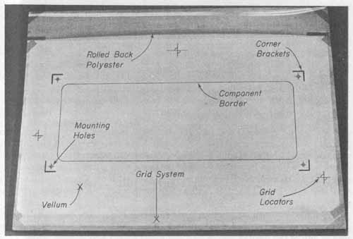
FIG. 2 Initial component layout.
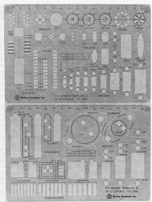
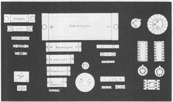
FIG. 3 (a) Set of 2 x scale layout templates for printed circuit design.
Courtesy of Bishop Graphics, Inc. Westlake Village, Calif. (b) Component
outlines (dolls).
Two types of aids in developing component layouts that are readily available are layout templates and precut component outlines. Figure 3a shows several common template styles. These templates, constructed of plastic, provide component outlines such as resistors, capacitors, transistor pin arrangements, and common integrated circuit patterns, thus eliminating the need, to some extent, of measuring individual terminal positions. These templates are available in scales of 1 : 1, 2 : 1, and 4: 1 to further aid the technician in layout work.
Component outlines, such as those shown in FIG. 3b, can easily be constructed from thin cardboard with the use of a scaled template, pencil, and scissors in any of the desired device and component sizes and shapes. These dolls provide an excellent means of establishing component placement, lead orientation, and component density within the component border of the layout. The technician should realize when preparing dolls that the leads of components such as transistors and ICs will be inserted into the insulated side of the PC board. The orientation of these leads must therefore be sketched on the dolls as if viewed through the top of the device and properly labeled (i.e., E to designate emitter and 1 to designate pin number 1 on integrated circuits). If this technique is not strictly adhered to, errors that cannot be corrected are certain to occur in the conductor pattern.
The cut component outlines are somewhat more desirable to use than tem plates since they allow for rapid movement and rearrangement about the grid system. The use of the template requires the technician to draw the desired component outline on the vellum. Any later change in position of any component or device means that the original outline will have to be erased.
Dolls used to establish the approximate component layout followed by the component outlines transferred to the vellum with the aid of layout tem plates allows for the most rapid and accurate results. Both of these layout aids are demonstrated later in this section.
The procedure for developing optimum component placement involves such considerations as size, weight, and heat-dissipation properties as well as the electrical criteria. This task, then, becomes quite complex and requires a meaningful approach for initiating layout. Three methods for solving this problem have been proposed. These are the schematic viewpoint, the central view point, and the peripheral viewpoint, which will be discussed here.
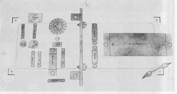
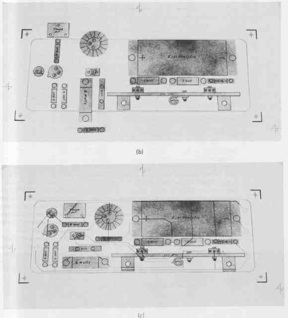
FIG. 4 Use of schematic viewpoint for component positioning: (a) doll
positioning using schematic viewpoint; (b) necessary rearrangement of
components because of physical limitation of component border; (c) final
component repositioning with conductor paths.
Since considerable care is taken by the draftsman in developing a schematic drawing to minimize crossovers and to present a well-balanced circuit layout, it seems logical that the first phase of component positioning would be to place the cut component outlines on the vellum in the approximate positions they occupy in the schematic diagram. Once the dolls have been positioned, the conductor pattern is drawn between components on the vellum to see that all electrical connections can be made without conductor crossovers. These crossovers would result in undesired electrical connections that do not appear in the schematic diagram. Conductor paths can be drawn on the vellum through component body outlines because the components will be mounted on the opposite side of the board from the conductor pattern when the pc board is assembled. Fig 4a shows the initial components placement as a result of employing the schematic viewpoint for the complementary-symmetry power amplifier board. Notice that some rearrangement is necessary because components and hardware exceed the component border and result in poor component density. When a component layout follows a schematic diagram exactly, the conductor pattern would be similar to that of the schematic. However, if even one component is rearranged, the conductor pattern should be checked and, if necessary, corrected in order to meet the electrical requirements of the schematic.
Components that present electrical or thermal problems are considered for repositioning first. For the example shown in FIG. 4, diode D must be repositioned so as to be mounted to the heat sink supplied for the complementary-pair transistors. This technique is to compensate for thermal instability. Mechanical problems are introduced in the initial positioning of this heat sink. Adequate heat dissipation of the output transistors will require a 2- by 3.5 inch sheet of aluminum. If mounted as shown in Fig. .4a, the width of this heat sink is greater than the opening provided on the chassis for mounting the board. From the chassis drawings, the allowable clearance between the top of the chassis and the enclosure is under 3 inches. This eliminates the possibility of the 3.5 -inch vertical position. The solution to this problem is to reposition the heat sink on the board as shown in FIG. 4b. The height of the sink remains 2 inches above the pc board and will mount easily within the enclosure. The repositioning of the heat sink means that the large output coupling capacitor and the two 0.47-ohm resistors must be repositioned parallel to the long edge of the pc board. FIG. 4b shows the component arrangement up to this point. The smaller components can now be rearranged. The completed component positioning and conductor path check is shown in FIG. 4c, which uniformly utilizes all the available pc board space and results in a balanced component arrangement. Notice that all resistors and capacitors are mounted either parallel or perpendicular to the edge of the pc board and that uniform spacing between components, whenever possible, is maintained. As will be seen later, positioning of components such as resistors and capacitors either parallel or perpendicular to the edge of ape board will aid significantly in laying out the final conductor pattern.
To complete the component layout, light position marks are made on the vellum around the dolls. With the dolls removed and with the aid of the under lying grid system, the drafting template is used to obtain accurate component size, position, and lead hole locations. It is important when drawing terminal pads that their centers are located on grid. When drawn properly, a vertical, arid a horizontal grid line will intersect at the center of all terminal pads, establishing the correct lead access hole spacing.
FIG. 5 shows the completed component layout drawing and final conductive paths for the power amplifier circuit. At this point, all components that require specific orientation or assembly on the finished board are keyed on the layout drawing. This technique involves the use of symbols such as a plus (+) sign to indicate capacitor polarity for electrolytics, (E) to represent the emitter lead of a transistor that could be positioned improperly, (1) to represent the number one pin of integrated circuits, as well as numerical and literal symbols to indicate external connections. By using this method of keying, once the corresponding end of a component or a particular pin or lead in a group is identified and positioned into the board, all other component leads associated with the key will be oriented in the correct location.
The second method of approaching the problem of component placement, termed the central component viewpoint, might be chosen over the schematic viewpoint if a single predominant component such as a transistor, integrated circuit (IC), or relay exists on the circuit schematic. The predominant component is first centered within the component border established on the vellum, using the grid as a guide. The support components, such as resistors and capacitors, are then oriented on the vellum, continually checking for correct electrical conducting paths. It should be pointed out that high-gain amplifiers require short input lead connections to eliminate possible noise from the input of the system. The support components are arranged to balance and make uniform the spacing around the IC. FIG. 6 shows a completed component layout for the IC preamplifier board together with all necessary keying information drawn on vellum.
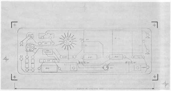
FIG. 5 Finished component and conductor pattern drawing using the schematic
viewpoint.
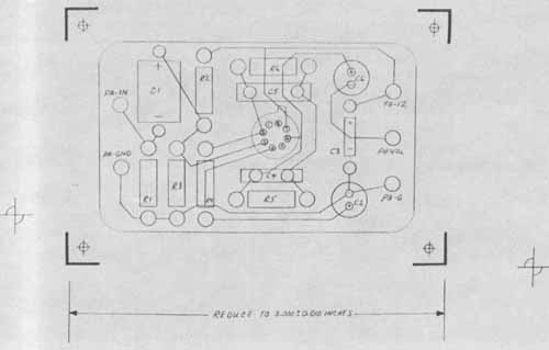
FIG. 6 Finished component and conductor pattern drawing using the central
component viewpoint.
The third method of component placement, termed the peripheral viewpoint is based on the initial planning stages of a package. If many of the circuit’s components will not be located on the pc board but instead will be mounted either on a chassis or front panel, this approach should be chosen for the pc board layout. The tone control circuit exemplifies this method. In this circuit, two potentiometers will be mounted on the front panel. Wiring from these panel-mounted components to the board can be greatly simplified if all pc terminal connections for these external leads are positioned near the potentiometers. To a great extent, the component placement on a pc board will be pre determined by these external connections. This is a common situation wherein the conductor pattern on a pc board is designed for input and output terminations at one end of the board to align with conventional plug- or receptacle-type printed circuit connectors. (See Section 14 for further discussion of connectors.) FIG. 7 shows the completed component layout for the tone control circuit board. Notice that all the terminals for potentiometer connections are along one edge of the board and that much of the closely associated circuitry is positioned close to these terminals.
The three methods of approaching the problem of component placement just examined are intended only as a guide to help minimize what may appear to be a formidable task. With experience, the technician will find his or her own approach to laying out ape board.
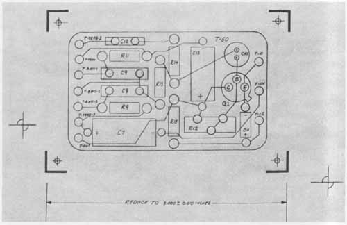
FIG. 7 Resulting layout drawing using the peripheral viewpoint.
Upon completion of the component and conductor pattern layout, the following observations should be noted:
1. The component and conductor pattern composite drawing enables the technician to readily observe both sides of the pc board simultaneously and therefore determine the effects of any layout modification on either side of the board.
2. Even though the component layout appears balanced and the conductor paths are electrically correct, there may be conductor pattern crowding. This crowding occurs when component placement forces many conductor paths to lie close together, resulting in nonuniform conductor density (i.e., making inefficient use of the total foil area). Although this condition may in no way impair circuit operation, the technician may choose to slightly modify components and/or conductor path arrangement to achieve conductor pattern balance. Proficiency in obtaining both component and conductor path balance simultaneously requires considerable layout experience.
3. Component spacing must be consistent with any specified spacing tolerances. For this, the grid system used to align and orient components is an immeasurable aid. Use of the intercepts of the grid system to position leads for components and external connections is also extremely helpful in minimizing misalignment of the eventual taped conductor pattern artwork.
4. Spacing among similar components, such as resistors, should be uniform to enhance the appearance of the board and to result in a more systematic drilling sequence.
It cannot be overemphasized that the appearance of any completed pc board is directly dependent on proper layout procedures. It is therefore imperative that this phase of design be undertaken with utmost care.
The final component and conductor path layout for the power supply board are shown in FIG. 8. This final layout completes all required pc drawings for the amplifier.
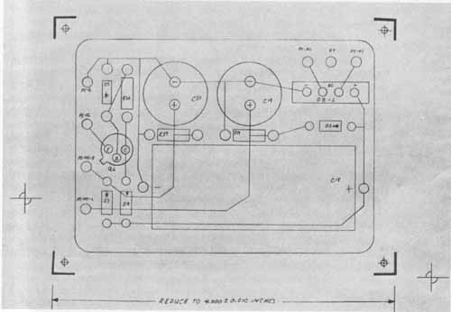
FIG. 8 Component layout drawing for the amplifier’s power supply board.
3. LAYOUT CONSIDERATIONS FOR AUTOMATIC ASSEMBLY
When designing a component and conductor pattern layout of a pc board that is to be assembled by automatic insertion, component placement is extremely critical and is governed by specific design criteria. To make automatic assembly cost effective, the designer must standardize the components selected for the circuit. By reducing the number of different size and shape axial and radial lead components, the variety of lead access hole spacings will be kept to a minimum. It is also important to arrange component positions on as few axes as possible, with rows and columns having uniformity of lead spacing and orientation. The optimum layout is where all components have the same lead span be tween terminal pads and are placed in columns and rows having all of their axes parallel. When more than one span is part of the layout, grouping of components of similar span where possible increases assembly efficiency by reducing worktable travel.
In most systems, the insertion head does not rotate. Because of this, component axes placed perpendicular to others reduce assembly efficiency since the board must be rotated 90 degrees to install these parts. In addition, no component axis should be positioned at a diagonal to any board edge.
As much as possible, component layouts should orient keyed components uniformly. For example, all notches on ICs that key pin 1 should face the same direction as well as placing the ICs in precise columns and rows.
For automatic insertion designs, boards must be provided with two tooling holes from which all lead access holes are placed on a fine grid in increments of 0.025, 0.050, and 1.00 inch. These tooling holes are later used to position the board on the automatic insertion machines. As in other designs, pad centers must be precisely located on grid.
Lead access hole sizes for automatic insertion are, in general, made 0.015 inch larger than those made for manual component assembly. This means that the diameters of the terminal pads should be increased by 0.030 inch to keep the same amount of copper surrounding the lead access holes. This surrounding copper is called the annular ring and is generally given a minimum-width specification, such as 0.012 inch.
In Section 14, Fig. 28 shows an automatic insertion head together with finger-to-lead and finger-to-body clearance for parallel-positioned axial components. The typical length and width clearances required for each guide finger are 0.100 and 1.30 inch, respectively. When axial components are placed side by side, as in Fig. 28, essentially no clearance is needed. However, to locate insertion holes on grid, the body center-line spacing of adjacent components is rounded off to the nearest 0.100 inch. When positioned end to end, a minimum of 0.100 inch between insertion holes is required.
The pad centers for adjacent ICs should have a minimum spacing of 0.150 inch. When they are positioned end to end, the spacing can be extremely small— as small as two times the manufacturer’s body tolerance.
4. DRAFTING AIDS FOR PRINTED CIRCUIT ARTWORK
The basic aids used for printed circuit artwork produced commercially are pre-cut pressure-sensitive adhesive tapes and conductor pattern shapes. These aids provide a quick and accurate method of developing artwork masters. Tapes normally used for single-sided pc board applications are available in opaque black and vary in thickness from 0.002 to 0.006 inch and in widths from 0.0 15 to 2 inches. FIG. 9 shows some common tape sizes used in pc artwork de sign. Although the selection of tape width will depend on such factors as cur rent, voltage, type of board insulation, board protective coating, and thickness of copper foil, some minimum specifications will be presented to serve as a guide in tape selection.
For general-purpose PC work, 1/16 (0.0625)-inch conductor width with a minimum spacing of 1/32 –inch is normally used with a 1:1 scale. Conductor width that are made or reduced to 1/32 (0.031) inch with a minimum spacing of 1/32 (0.031) inch often are used for small signal circuits with low power characteristics. For 4: 1 and 2: 1 reductions, tape widths of 0.125 inch and 0.0625(1/16) inch, respectively, are employed to obtain a final reduced conductor width of 0.031 inch. These larger tape widths are easier to handle and yield a more accurate artwork master. It is recommended that the beginner not select a tape width of less than (0.031) inch because of the difficulty in handling and the care that must be exercised to manipulate these narrow widths. For 1 : 1 art work masters, tape widths of 2 (0.03 1) inch are preferable when dexterity and electrical characteristics permit this size. Otherwise, a max of 0.0625 inch should be used. Drafting aids for lead patterns associated with transistors and integrated circuits are more readily available in 2: 1 and 4 : 1 scales, so it is preferable to work in either of these two scales. A scale of 1 : 1 should be limited to circuits not employing intricate wiring associated with transistor and integrated circuit devices. A 5: 1 scale is only used when an unusually high degree of accuracy is required. From the standpoint of economy, the 2 : 1 scale is preferable to the 4: 1 scale.
The foregoing information does not necessarily conform to any particular military or industrial specifications but presents realistic and practical tape sizes that are suitable for general-purpose applications. For more detailed information relative to tape width as a function of current capacity, refer to TABLE 7.
Many precut tape configurations as well as tapes for conductor paths are available. FIG. 10 shows many of the most common of these outlines. A brief description of each with their application follows.
Terminal pads, also called teardrops, are available in all common conductor widths. They are filleted at the terminal ends and are available in single-end entry, double-end entry, and elbow angles to facilitate the layout work. Lead hole diameters should be selected to be no greater, when reduced, than the component lead or wire they are to accept. The radius of the conductor pad should be at least three times the lead hole diameter. In addition, the entry width (dimension A in FIG. 10) should be the same width as the tape used for the conductor path.
If smooth curves cannot be made by simply bending the straight tape during application, precut elbows with angles of 30, 45, 60, and 90 degrees, or universal circles, may be used. These aids are shown in FIG. 10. Universal circles provide not only various bend radii, but also an infinite number of angles by cutting the appropriate circle to the desired angle. If narrow tape is used, conductor path direction can be changed by forming the tape into a smooth radius. Each size and type of tape has a minimum bend radius. Exceeding this mini mum narrows the tape width. The minimum radius for each tape size can be determined by observing the smallest bend that can be formed without causing the tape to buckle along the inside edge of the bend or stretch along the outside edge. The minimum bend radius is approximately the width of the tape used. Stretching the tape between two points should also be avoided since the tape will tend to creep, thereby altering the position of the conductor path or creating gaps in the path. Conductors that meet at right angles to each other may be filleted. For this purpose, tees with the same entry widths as the conductor are used.
Terminal circles or donuts are commonly used in layout work for locating holes and are selected according to the same criteria as are terminal pads.
Special shapes for mounting the common transistor and integrated circuit case configurations are also shown in FIG. 10. Included are terminal pads for the TO-5 3-lead transistor, the TO-5 8 and 10 lead IC, the 14-pin dual-in-line IC, and the 14-lead flatpack. Many more precut drafting aids are available. All of these shapes are mounted on a pressure-sensitive adhesive backing ready for application.
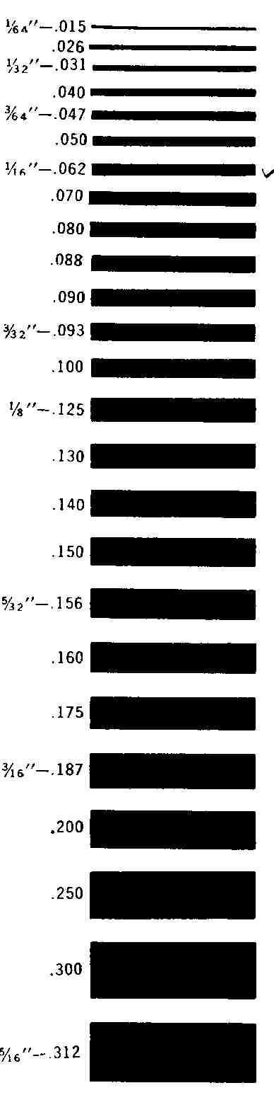
FIG. 9 Common tape widths used for printed circuit artwork designs.
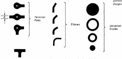
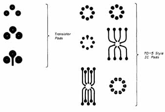
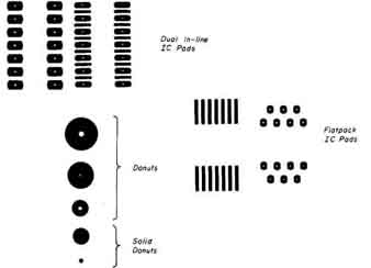
FIG. 10 Precut tape configurations. Courtesy of Bishop Graphics Inc.,
Westlake Village, Calif.
Connector patterns, also shown in FIG. 10, are of three basic types: spaced-edge (finger), staggered and in-line. The use of these aids saves considerable time by eliminating repetitive taping. The spaced-edge pattern, often referred to as terminal connector strips, is used with insertion-type board-edge receptacle connectors. If a connector plug that mounts directly onto the pc board and has contact pins either swaged or soldered to the conductor pattern is used, a staggered or in-line type donut configuration is required, the choice of which will depend on the type of contact pin arrangement on the plug. (See Section 14 for a discussion of various connectors.) The connector patterns, shown in FIG. 10, are accurately scaled for standard printed circuit connectors or plugs. These precision-spaced aids are available on a transparent pressure-sensitive adhesive acetate film for group unit application. Strips of up to 18 pads (donuts) or 22 edge connectors are available, which may be cut to the desired number.
Board delineation marks are used to outline the board’s overall dimensions and to position the reduced artwork accurately onto the board for processing. These aids are positioned along the outside edges of the grid lines representing the four corners of the board. These marks are used as guides only and are not processed onto the finished pc board.
Grid locators (targets or bull’s-eyes) are used to align one master accurately over another when developing solder masks, marking masks, or double- sided board layouts. These targets are positioned outside the board delineation marks and are not an integral part of the finished pc board.
Arrowheads are used in conjunction with numerals that designate art work reduction dimensions. A whole number with the appropriate tolerance is positioned in the center between two vertical pieces of tape on the artwork. The tape is separated by a distance approximately as great as that which is between the delineation marks. The arrowheads are positioned with their points against the inside edges of the vertical tape. This technique is shown in FIG.
The precut tapes discussed are an illustrative selection and do not constitute a complete listing. Nonstandard-device outlines, such as the keyed-type transistor pattern shown in FIG. 10, are available from some manufacturers on special order but are uneconomical unless large quantities are used. For additional standard drafting aids, appropriate manufacturers’ catalogs may be consulted.