AMAZON multi-meters discounts AMAZON oscilloscope discounts
LEARNING OBJECTIVES:
Upon studying this section on techniques of quality assurance procedures for printed circuit boards, the student should be able to:
1. Understand the difference between destructive and nondestructive testing.
2. Use an inspection magnifier lamp to visually inspect a pc board.
3. Repair breaks in conductor paths.
4. Repair bridges between pattern features.
5. Use a comparator to measure pattern features.
6. Visually recognize hole-plating defects.
7. Use precision instruments to measure pc boards.
8. Use an ohmmeter to perform basic electrical testing.
9. Be acquainted with automated test equipment.
10. Microsection, inspect, and evaluate specimens from a pc board using a high-powered microscope.
11. Use a microscope to take precision measurements.
0. INTRODUCTION
The manufacture of a printed circuit board, whether it be a single-sided, double- sided, or multilayer design, requires many sequential processing steps, expensive equipment, and a considerable amount of materials and chemicals. Because of the numerous processes, some of them being quite critical, a finished pc board is prone to a host of faults. Problems such as defective materials, incorrect processing sequence, errors in chemical timing or temperature, and poor workmanship are not uncommon and never completely unavoidable. A fabricated pc board represents a significant cost to the manufacturer. Many detected defects are either correctable or acceptable and may not render a board useless. In addition, the components that are to be installed onto the board represent further major costs. For this reason, it is not economically sound to load a board that has not been inspected and tested to determine its acceptability. In this section we establish inspection procedures which will determine the quality of a processed board before the component assembly and final soldering processes are initiated.
It is not the intent of this section to define the absolute criteria for accepting or rejecting a processed pc board. These criteria are determined by the manufacturer of the product which is based upon the system’s functionability and the standards of acceptability as defined by the pc board industry. The objective of this section is to identify the common features of a processed board to be inspected and to show the most appropriate method of determining the relative quality of these features. In many cases, a common problem is in interpreting the results obtained in the inspection procedure.
In general, inspection procedures for pc boards can be separated into two major categories: (1) nondestructive testing and (2) destructive testing. As the terms imply, the nondestructive test performed will not damage the board which is functional after inspection. This is the most cost-effective method of board testing. However, to accurately determine the quality of manufacture, a destructive test is necessary.
Nondestructive tests presented in this section are (1) visual, (2) mechanical, and (3) electrical. Visual inspections are those which can be made with the naked eye or with the aid of a magnification device. Mechanical inspection primarily involves the checking of measurements of length, width, thickness, and hole diameters. Electrical inspections can involve such tests as checking for short or open circuits on conductor patterns or within the inner layers of multi- layer boards. Some of these tests use sophisticated computer systems that completely check the electrical pattern for any defects.
To properly test a pc board, all three methods, visual, mechanical and electrical, should be employed.
The treatment of destructive testing will include the preparation and interpretation of microsectioned samples of plated-through holes.
1. VISUAL INSPECTION
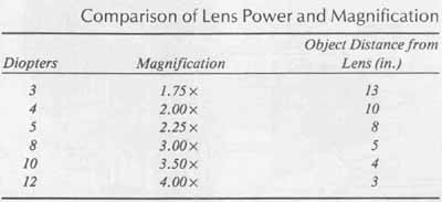
Even though the finished pc board can be inspected with the naked eye, an inspection magnifier lamp is an ideal aid. This instrument more readily allows the detection of flaws and results in less eye strain. The magnifier lamp has a circular 22-watt fluorescent tube which encircles an interchangeable magnifying lens. Typical lens powers are 3, 4, 5, 8, and 10 diopters (1.75 to 3.5 x), which provide shadow- and distortion-free viewing. The lower-powered lenses are used for viewing a reasonably large area, while the higher-powered lenses are used for closer scrutiny of a smaller area or feature. See TABLE 1 for a comparison of lens power and magnification.
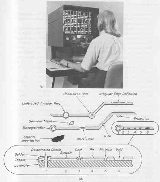
An inspection magnifier lamp used to inspect a pc board is shown in FIG. 1. The types of surface defects readily visible under a magnifying lamp are broken circuits and bridged circuits. Broken circuits are viewed as obvious interruptions in conductor paths such as that shown in FIG. 2a. These may be the result of improper handling of the taped artwork master or the phototools, opaque particles allowed to remain on the phototools, incomplete developing of the resist film, or scratched pattern-plated solder before the etching process. This type of defect must be repaired. If the number of such defects is not extensive and if it is permissible by company policy, the break can be repaired with bus wire. A piece of bus wire cut long enough to be laid along and span the broken path serves as a conductive bridge. Flux is applied to the paths on each side of the break and with the wire held in place, it is soldered to the broken ends of the conductor paths. The result of such a repair is shown in FIG. 2b. The flux should be completely removed after the wire has been soldered. (Note: This type of repair should be undertaken after the pc board is completely assembled and soldered.)
--- TABLE 1 Comparison of Lens Power and Magnification
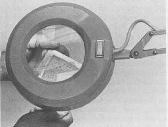
---FIG.—1 Inspection of pc board under magnification.
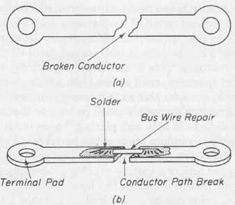
---FIG.—2 Typical conductor defect and repair: (a) open circuit; (b)
one method to repair open circuit.
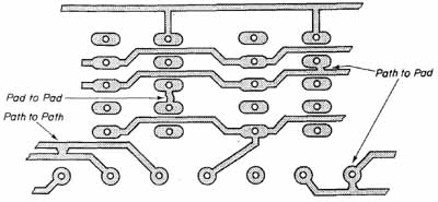
---FIG.—3 Examples of circuit bridges.
Bridged circuits appear as unwanted connections between any features in the conductor pattern (see FIG. 3). These shorts are again primarily due to improper handling of the artwork masters, the phototools, or of the imaged board. A scratch in the photo-resist can also cause these bridged circuits to form. If permissible, these defects can be easily repaired by removing the unwanted metal (solder over copper plating over laminate copper) down to the insulation surface with a scalpel.
When visual inspection requires the precise measurement of the conductor pattern features, an important device used for this purpose is the 10 x magnifier called a comparator. This has a precisely scaled reticule such as the one shown in FIG. 4a. As shown in FIG. 4b, the scale has 100-mil (0.1-inch) major divisions with 25-mil (0.025-inch) subdivisions and 5-mil (0.005-inch) minor divisions. The comparator is designed with a transparent 360-degree base to admit a maximum amount of light. It is used by simply centering its base directly over the feature to be measured. By careful alignment of the reticule on the feature, its size can be precisely determined to within 5 mils and a good reading to within 1 or 2 mils can be estimated.
The use of a comparator is shown in FIG. 4c, d, and e. FIG..4c shows the conductor path width being measured. Note that the width distance falls precisely on a minor subdivision, resulting in an exact measurement of 15 mils (0.015 inch). FIG..4d shows a comparator being used to measure the annular ring of a pad. Here the result is less precise since the dimensions of the feature span between minor divisions. However, a reading of approximately 7 to 8 mils (0.007 to 0.008 inch) can be closely estimated. Notice also in FIG. 4d that there is some misregistration of the pattern since the terminal pad is not centered on the hole as seen by the nonuniformity of the annular ring. Another example of the use of a comparator is the measurement of the air gap between conductor pattern features. This is shown in FIG. 4e, where a conductor path-to-terminal pad spacing is read as less than 5 mils. A minimum air gap of this dimension may be questionable as to its acceptability.
A severe imperfection on double-sided pc boards that can be detected by visual inspection is defects in hole wall plating. These voids are the absence of both solder and copper in random areas of the barrel (see FIG. 5a). These are often the result of excessive cleaning prior to pattern plating, incorrect processing of the deposition line, or a variety of other processing problems. Voids in a plated-through hole may well render the board useless. Usually, one or two random and isolated voids can be considered acceptable, but if they appear in the same hole, they most likely exist in all holes and in all boards processed in that batch.
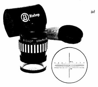
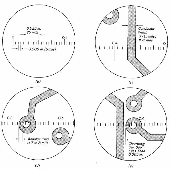
--- FIG.—4 Measurements that can be made using a comparator: (a) 10
x comparator, courtesy of Bishop Graphics Inc., Westlake Village, Calif.;
(b) scaled reticule; (c) conductor width measurement; (d) annular ring
measurement; (e) air gap measurement.
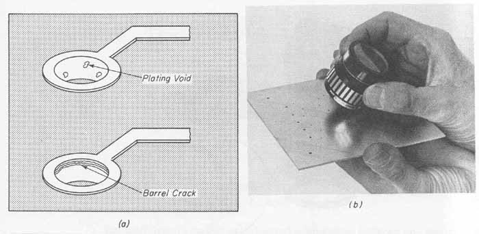
--- FIG.—5 Plating defects and methods of visual inspection: (a) voids;
(b) inspection using comparator at a 45-degree angle; (c) optical hole
inspector, courtesy of ALCHEMITRON.
Another form of void, also shown in FIG. 5a, is a rim void or barrel crack, which occurs at the interface of the surface of the hole and the top or bottom ends of the barrel. These cracks are totally unacceptable since they break the electrical continuity between both sides of the board. Voids can often be detected with the naked eye by viewing the holes at a 45 degree angle to the board surface. A comparator may also be used to enhance the view. It is also placed at a 45-degree angle to the board surface (see FIG. 5b).
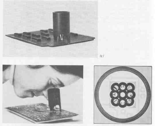
A special magnifier, used exclusively for the inspection of plated-through holes, is shown in FIG. 5c. This 8x magnifier has a center prism that splits the image of the inside of the hole into nine views that simultaneously show the entire surface area of the barrel without moving the instrument. It is simply placed flush to the surface of the board and centered on the hole to be inspected. Thus a 360-degree undistorted view of the barrel is achieved without rotating the board or the instrument.
Inspection of plated-through holes also detects foreign matter, such as dust and dirt, which may have resulted from drilling, or from nodulation (rough surface) caused by poor plating processes. Anything on the hole walls other than a smooth and continuous layer of metal is an indication of processing problems starting with the drilling operation.
--- FIG.—6 Defects are more readily found by magnified optical inspection:
(a) optical inspection, courtesy of Circuit Equipment Corporation, Baltimore,
Md.; (b) conductor pattern defects.
Highly sophisticated optical equipment is also available to improve the inspection of a pc board. One such instrument is shown in FIG. 6a. It is designed to project a magnified view of the pc board onto a large screen. It includes a microscope to permit even closer examination of any selected feature. This inspection system is equipped with an indexing x-y table onto which the board to be viewed is placed. The entire area of the board can be rapidly and systematically scanned at as much as 25 x magnification. Sufficient space is available to allow some minor repairs to be made within the viewing area. One of the advantages of this type of inspection system is that it can aid in viewing conductor pattern defects which may not easily be detected by eye or with the aid of low-magnification devices. Some of these defects, together with those previously mentioned, are shown in FIG. 8b. In addition to inspecting finished pc boards, these optical inspection systems may also be used to check and correct artworks and phototools. This greatly aids in preventing a number of board defects that might otherwise occur.
2. MECHANICAL MEASUREMENTS
Mechanical measurements on pc boards may be grouped into two general categories: (1) the measurement of board length, width, and thickness, and (2) hole size measurement of both plated and unplated holes.
The length and width of the finished board should be measured with precision instruments such as the dial caliper shown in Fig. 3.9. This caliper is typically accurate to 0.001 inch, which is suitable for making board measurements. The results of the dial caliper readings should be compared with those of the dimension drawing of the board to determine if they are within the specified tolerance. For single- and double-sided boards, the length and width dimensions are critical, especially if the board is to slide into grooved guides, shown in FIG. 24, so that its fingers fit into an edge-line connector. On the other hand, if the board is designed to simply be installed into a chassis, such as our amplifier shown in FIG. 25, its dimensions are far less critical.
In the case of a multilayer board, the thickness dimensions are extremely important if the fingers are to fit snugly into a connector. To avoid mechanical or electrical problems, the board must not be thicker or thinner than the specified tolerance. Thickness measurements can also be accurately made with the dial caliper or with a micrometer. These measurements should be taken in the finger area to determine correct fit into the connector. To obtain the most accurate reading, only the insulation thickness should be measured, not a portion of the board that contains any copper pattern. If thickness measurements of all four corners of a multilayer board show a wide variation, the problem is usually the result of a fault in the press platens.
For the accurate measurement of unplated holes having straight sides (i.e., uniform top-to-bottom diameters) a dial-indicating tapered-pin hole gauge, such as the one shown in FIG. 7a, may be used. To measure the hole’s diameter, the tapered pin is first inserted into the hole. The base of the gauge is then brought down flush to the insulation surface of the board (see FIG. 7b). The dial indicator is calibrated to read the hole diameter directly as a result of reading the diameter of the tapered pin at its top entry point. The gauge shown in FIG. 7a will provide a hole-diameter reading to an accuracy of 0.001 inch. Four different gauges of this type will give a full range of measurements from 0.010 to 0.330 inch, which represent drill bit sizes from No. 80 (0.35 mm) to 3/8-inch (9.5 mm).
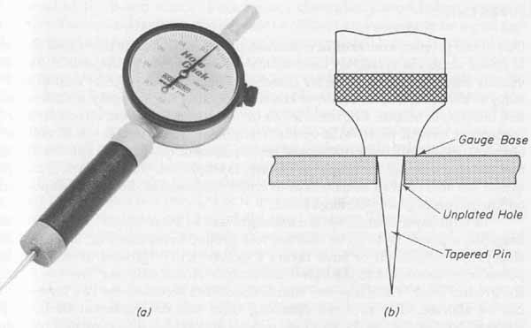
---FIG.—7 (a) Tapered-pin hole gauge, courtesy of ALCHEMITRQN; (b) measurement
technique for unplated holes; (C) measurement technique for plated holes.
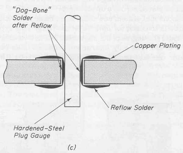
A cross-sectioned view of a drilled hole that has been plated and reflowed is shown in FIG. 7c. Note the hourglass or dog-bone effect of the plated metals. A major concern in plated holes is that the specified component leads fit into the holes without any degree of difficulty. Accurate measurement will determine this in addition to ensuring that proper plating thickness has been achieved. To measure the minimum diameter of these nonuniform barrels, a set of untapered plug gauges, having accurate and uniform diameters, must be used. Typical sets of plug gauges for this application, such as those available from the Meyer Gauge Company, consist of a series of 2-inch microfinished hardened-steel pins. One set ranges in size from 0.011 to 0.060 inch in diameter, increasing in increments of 0.001 inch. Another set ranges from 0.061 to 0.250 inch, increasing in the same increments. The size of pin which when inserted into the hole will meet extremely slight resistance or drag indicates the hole’s diameter. These pins must be used with care. If even moderate pressure is required to insert a pin into the hole, damage to the plating could result.
3. ELECTRICAL MEASUREMENTS
One of the primary concerns in a finished pc board is that no unwanted shorts or opens exist. For relatively uncomplicated designs, visual inspection, as previously discussed, is suitable for detecting these faults. A great deal of difficulty is encountered, however, in the inspection of high-density double-sided and multilayer boards. For these levels of designs, it is beyond effective visual inspection, even if aided with optical equipment. After initial visual and mechanical inspection, computer-based test equipment designed to automatically test the entire circuit for proper continuity is employed. Other electrical instruments are also used to measure the average thickness of the copper deposited on the barrels of plated-through holes.
In multilayer boards, severe misalignment of inner layers may cause, for example, a power layer to be shorted to a ground layer (see FIG. 8a). Note that proper alignment of inner layers 2 (power) and 3 (ground) results in the power layer connected to the barrel and an open circuit existing between it and the ground layer. Thus, a power source connected across these two layers will not be shorted. The problem resulting from the misalignment of layer 3 (ground) is shown in FIG. 8b. Here, ground makes electrical connection to the barrel, resulting in its being shorted to layer 2 (power). Because the power and ground layers are connected through the barrel, a power source connected to these points will be placed across a direct short.
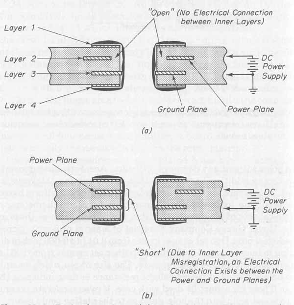
--- FIG.—8 Testing for an internal short circuit in an MLB: (a) properly
aligned inner layers; (b) mis-registration of power plane. “Open” (No
Electrical Connection between Inner Layers)
For the reasons just stated, one of the most basic electrical tests made on multilayer boards is to check for inner-layer shorting. This type of test is not intended to measure the degree of misalignment but determines the acceptance or rejection of a board. The only instrument required is an ohmmeter. After zeroing the meter, one test probe is brought into contact with an outer-layer terminal of the board which is connected, through a plated hole, to layer 2 (power). The second meter probe is made to contact an outer-layer terminal pad that connects to layer 3 (ground) through another plated hole. A reading of infinite ohms (i.e., an open circuit) should be read on the ohmmeter which indicates an acceptable board. This reading shows no electrical connection existing between layers 2 and 3. Power can safely be applied to this board. If, however, the ohmmeter reads zero ohms (i.e., a short circuit between power and ground layers), the board must be rejected because of inner-layer misregistration. Any power applied to these inner layers will result in the supply being shorted, causing fuses to blow, circuit breakers to trip, and so on.
Recent demand for higher-density boards and the number of layers required in one board has resulted in it becoming impossible to test, with 100% accuracy, the electrical integrity of the total pattern. The use of the most sophisticated visual inspection techniques coupled with mechanical tests and electrical checking with meters is found to be unsuitable for high-density, ultra- fine-line boards. Not only is this type of testing extremely time-consuming, but only 50 to 70% of faults in a multilayer board are detectable, due to human limitations. To overcome these shortcomings and to develop test equipment more compatible with the state of the art, manufacturers have developed a new concept in the electrical testing of bare boards (i.e., boards that have no parts mounted). This automated test equipment (ATE) uses a computer which can be programmed to quickly and repeatedly test 100% of the conductor pattern on any level of the board. It can locate faults (shorts or opens) and identify the type of fault. Bare-board testing equipment is classified as either dedicated or universal systems. They are intended for the testing of large volume work and not for prototype applications.
A bare-board pc board test system is shown in FIG. 9a. It consists of a microprocessor-based computer connected to a multiple-contact test fixture or head through a wire cable system. Additional equipment required is an external vacuum pump to activate the test head and a printer to provide a readout of the test results. The test head is manufactured to test a specific circuit board pattern (dedicated) or designed to test any pattern (universal). A universal text fixture is far more expensive than the dedicated type. For both test fixture de signs, the head consists of a series of spring-loaded test probes or nails. They are press-fitted into an insulated base plate in a pattern which aligns each nail to make contact with each terminal pad of the conductor pattern. Several styles of test probes are shown in Fig 9b. The probe with the serrated top is the one used in the tester shown in FIG. 9a. This style makes a firm electrical contact on its assigned terminal pad. The other end of the probe is connected to a lead in a cable which is connected to the computer. The cable provides the electrical connections between the individual terminal pads and the microcomputer.
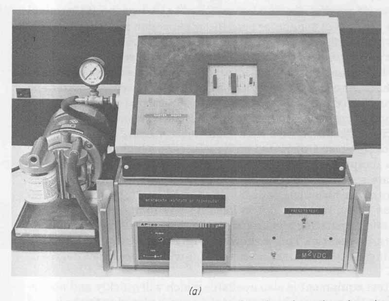
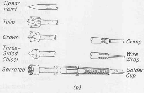
--- FIG.—9 Electrical testing of bare boards: (a) bare-board test system;
(b) styles of contact pins.
A second insulated panel rides on guide pins secured to the base plate. This panel is provided with a clearance hole for each contact point (i.e., pad) and is fitted with tooling pins for registering the board to the bed of nails (see FIG. 10). After the pc board is positioned onto the tooling pins, a sheet of surgical rubber is placed over the head to create a vacuum seal on the board. When the vacuum system is activated by the computer, the board is forced downward onto the bed of nails to make electrical contact with each terminal pad.
A dedicated test head has test pins located below each individual terminal pad for a specific conductor pattern only. On the other hand, a universal test head has a test probe positioned on a grid spaced at 0.1-inch intercepts. Large universal test systems may have a matrix of as many as 40,000 probes (20- by 20-inch grid). With this type of system, any board design may be tested as long as its terminal pad centers are located on a 0.1-inch grid and the tooling holes on the board are made to align with the tooling pins on the fixture. To test a specific conductor pattern on a universal test system, a plexiglass plate with a hole image that matches the terminal pad locations is positioned between the probe matrix and the board. This allows only those probes that align with pads to make contact with the board, while the other probes are blanked out.
The bare-board tester, shown in FIG. 9a, has two modes of operation. These are the learn mode and the test mode. When power is initially applied to the microcomputer, the system is in the learn mode. A pc board having a predetermined correct conductor pattern is placed on the test head. The press to test button is depressed, which activates the vacuum system and causes the board to be pressed against the probes. The microcomputer then samples each test probe and stores in its memory the number assigned to each probe, its terminal pad position, and the correct conductor path interconnection sequence. The microcomputer has thus sampled each test probe and learned the electrical continuity map of the correct master board. This board is then removed from the test fixture and the system is ready to electrically test boards which have been processed with the same conductor pattern as the master board. A board to be tested is placed on the fixture and the press to start button is again activated. The contacting probes feed information to the computer, which compares the conductor pattern of this board with that of the master board stored in memory. The results of this test are printed on a paper tape which indicates if the unit under test is acceptable (no shorts or opens) or if there are any faults. Any shorts or opens are specified together with their locations by identifying the assigned numbers of the terminals pads involved (see FIG. 11a). To most efficiently make use of the tape readout in locating any faults on the board, a layout of the conductor pattern, together with the assigned terminal pad identification numbers, is essential. This is shown in FIG. 11b. It can be seen that a bare-board testing system is quick and repeatable with a consistent degree of accuracy.
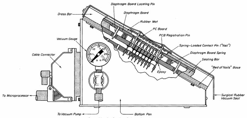
--- FIG.—10 Sectional view of test head.
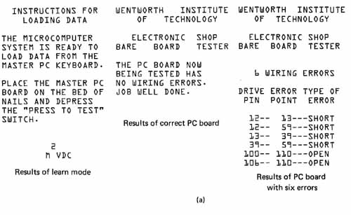
--- FIG.—11 Bare-board conductor pattern code and results of automatic
testing; (a) bed of nails printouts; (b) terminal pad identification.
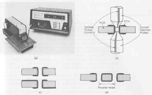
--- FIG.—12 Nondestructive testing of plated-through holes: (a) Caviderm,
courtesy of UPA Technology, Inc.; (b) self-centering conical test probes;
(c) isolated PTHs do not result in parallel paths; (d) parallel holes
closer than i-inch spacing will result in incorrect readings.
Automatic test equipment is also available which will quickly and nondestructively measure the average thickness of the copper plated onto the barrel of a plated-through hole. One such system is shown in FIG. 12a. This computerized tester is called the Caviderm CD7 and is manufactured by UPA Technology, Inc. The Caviderm makes a microresistant (KR) measurement which can be used to nondestructively test both the quality as well as the plating thickness of a plated-through hole. The equipment consists of two self-centering conical contacts which touch the top and bottom rim of the hole (see FIG. 12b). The current injection cones apply a precisely known current (usually 20 mA) through the copper plating which makes up the hole wall. The resulting voltage drop developed across the hole is detected by the voltage pickup contacts. Electronically, the voltage developed is divided by the current injected to result in micro-ohms of resistance (R = V/I). The computer processes this data and translates it automatically into barrel thickness, shown on a digital display in mils. This method of test actually measures the average resistance or average thickness of the barrel. For this reason, any voids, cracks, or thin spots will strongly influence the reading. The net result will be lower values of wall thickness displayed than those specified or that would result if these defects were not present. In testing of plated-through holes in either double-sided or multi- layer pc boards, the measurement is essentially the copper thickness and is not really effected by the solder layer above the copper. The measurement can, however, be misleading if not performed correctly. For measurements to be ac curate, an isolated hole must be used. Shown in FIG. 12c, an isolated hole is one that has either no circuit etches (top or bottom) leaving the hole, or any hole having interconnecting terminations that do not result in a parallel circuit. An inaccurate reading will also result if the hole to be measured forms a parallel circuit with a hole closer than inch (see FIG. 12d).
The Caviderm CD7 tester is self-calibrating. All that is required to initiate the measurement is to key into the computer the board thickness and the hole diameter.