AMAZON multi-meters discounts AMAZON oscilloscope discounts
4. MICROSECTIONING
All of the pc board inspection and test techniques discussed to this point are nondestructive, that is, the board has not been physically damaged in any way. These tests are essential for ensuring a degree of quality control. However, non destructive testing falls short in providing the product user or the manufacturer a complete assurance of the quality of the finished pc board. This assurance can only result through a destructive cross-sectioning test procedure called microsectioning. In this type of test, a sample board from a production lot of double-sided or multilayer boards is destroyed in order to accurately view the interior walls of a plated-through hole to determine its quality. Microsection testing can also be performed using a specially prepared sample, called a coupon, which does not require that a finished board be sacrificed. This nondestructive microsectioning test will be discussed in conjunction with specimen selection procedures.
Visual inspection of the cross-sectional view of the barrel of a typical plated-through hole requires the use of a microscope having a minimum of 50 x magnification. This highly magnified view allows the electrical integrity of the interconnection points between the top and bottom ends of the barrel to be more accurately evaluated. Plated-through holes are the most critical processes in the fabrication of a pc board. Continuous metal must be formed through the hole and over the original copper outer surface.
Microsectioning aids in evaluating a variety of plated-through-hole characteristics, including barrel copper and solder thickness, voids, barrel cracks (rim voids), nodulation (rough plating), annual ring, conductor width, multi-layer board registration, epoxy smear, and etchback. (These defects and their appearance will be discussed later in this section.) The visual evaluation of these characteristics provides the end product user with a more definitive representation of the quality of the finished board. Used as a means of quality control, microsectioning tests are an early warning indicator to the manufacturer in determining potential processing problems. If allowed to go undetected, these problems can dramatically reduce the yield of acceptable boards.
The following steps outline the microsectioning process:
1. Specimen selection and removal. A sample plated-through hole is selected and then removed from the board with a punch.
2. Cross-sectional cutting. The cross-sectional side view of the hole is pre pared for inspection by sawing through the center of the hole using a diamond saw.
3. Specimen mounting. The cross-sectional view is positioned in a mold which is next filled with an epoxy mounting material and allowed to harden. The epoxy-mounted sample is then removed from the mold.
4. Sanding and polishing. The surface to be inspected is sanded and then finely polished to a smooth finish.
5. Specimen etching. The area to be inspected is lightly etched to remove any smearing of the two metals (copper and tin-lead) so that they may be clearly distinguishable.
6. Microscope inspection. The specimen is now ready to be viewed on an inverted microscope.
Each of these steps will be discussed in detail followed by an evaluation of several illustrations showing typical plated-through-hole faults.
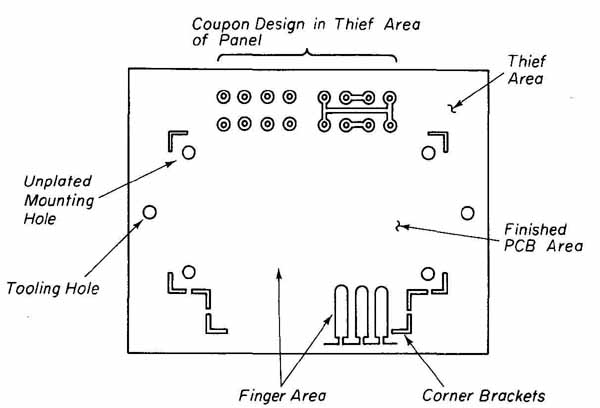
--- FIG.—13 Test coupon provided in thief area eliminates board destruction.
Specimen Selection and Removal. The selection of a sample specimen may be made from the image area of a pc board or from a specially prepared coupon within the thief area (see FIG. 13). Those selected from the image area will result in the board being destroyed. Samples taken from the thief area will not damage the board, allowing it to be returned to the usable lot. It is thus apparent that there is a substantial cost advantage in selecting samples from coupons in the thief area. The disadvantage, however, is that the thief area is the section of the board having the highest current density. This will result in a hole having a larger plating thickness than one appearing in the image area. Either sample will show essentially the same degree of plating quality and registration.
Which of the sample areas to select becomes a trade-off of cost versus inspecting a more representative sample (i.e., taken from the image area). This trade-off usually results in inspecting for plating quality and registration by using thief area coupons and occasionally destructively sampling a note from the pattern area to monitor copper and solder thickness.
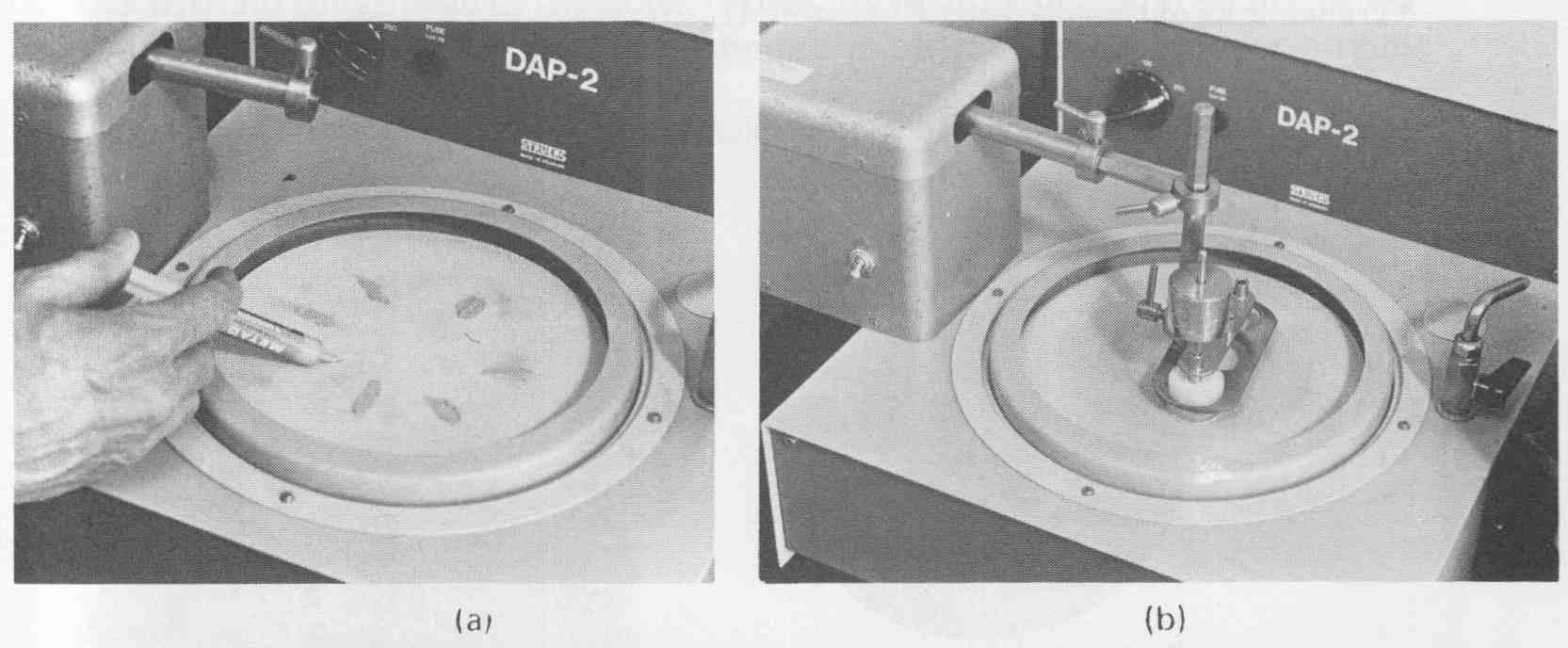
Specimen Removal. When removing the plated-through-hold sample from the pc board, extreme care must be exercised to avoid damaging the plating. Any deformities or cracks resulting from its removal will render the sample useless in evaluating the quality of the plating. Specimen holes may be removed by sawing, shearing, or punching. On 0.059-inch boards, punching is the method most often used. A specially prepared strain relief punch and standard die, as shown in FIG. 14a, are required. The diameter of the punch should be at least inch with a -inch-diameter relieved center having a depth of 0.1 inch. This arrangement can be used in a single-station punch press or a standard lever-operated turret punch such as that shown in Fig. 6.14. To remove the sample, the board is positioned in the machine between the punch and die as shown in FIG. 14b. With the specimen hole centered under the relieved section of the punch, it is removed from the board with no damage resulting to the barrel plating. This method of specimen removal is quick, easy, and effective.
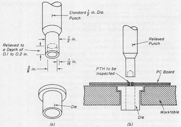
--- FIG.—14 PTH specimen removal by punching; (a) specifications for
relieved punch for specimen removal; (b) removing sample PTH for inspection.
Cross-Sectional Cutting. With the specimen removed, it is next cut through the hole slightly below its center line using a precision cutoff saw fitted with a diamond-coated abrasive blade. A typical saw used for this purpose is shown in FIG. 15a. The sample is firmly clamped into the cutoff arm in a precise position over the blade so as to bisect the hole. A micrometer adjustment is used for this positioning. The cutoff arm is weighted with approximately 75- to 100-gram weights in order to apply an adequate downward pressure of the sample against the saw blade during the cutting operation. The speed of the blade rotation is set to about 75 rpm. (This corresponds to a setting of 3.5 on the unit shown in FIG. 15a.) The sample is then gently lowered until it rests against the rotating blade. The bottom edge of the blade is continuously immersed in a mineral oil cooling bath in order to avoid the generation of heat during the cutting process, which could adversely affect the appearance and characteristics of the hole plating. With this type of cutting arrangement, bisecting of the sample takes between 2 and 3 minutes and results in an extremely smooth-cut edge. After the cut is complete, the saw will automatically shut off. The sample is then withdrawn from the clamp and washed in alcohol to remove all traces of the coolant. The cut sample is shown in FIG. 15b.
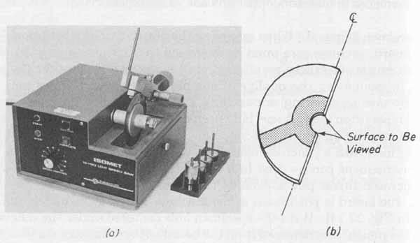
--- FIG.—15 Cutting specimen to expose cross section of PTH with a diamond
saw: (a) diamond saw; (b) cut specimen.
Specimen Mounting. To prepare the specimen for sanding and polishing, it is encapsulated in an appropriate mounting compound. This begins by positioning the sample against a piece of glass with the hole to be viewed (i.e., the cut edge) facing the glass. It is secured in this position with a retaining spring, as shown in FIG. 18a. A plastic mounting ring, which has been sprayed with a silicon-base mold-release agent, is then centered around the sample. To pre vent damage to the outer-layer plating during the sanding and polishing process, the mounting ring is filled with an encapsulating compound. This also provides support to the cut edges of the plated hole. The encapsulating material must be a cold-mounting compound that will harden quickly. Materials that require high pressure and elevated temperatures are unsuitable for pc board inspection applications since they can damage the plating. A product called Quick MOUNT is an effective cold-application compound consisting of a powder and liquid resin. To mix this material, 1 part by volume of the liquid resin is poured into a paper cup and 2 parts of the powder are added. This is stirred with a spatula for at least 1 minute to result in complete mixing. The compound is slowly poured into the mounting ring until it is almost full. To prevent the sample from moving while the compound is being added, it may be held in place with a thin rod (see FIG. 16b). The filled mounting ring is then allowed to stand undisturbed for a minimum of 30 minutes at room tempera ture. The mixing of cold-mounting compounds may cause air bubbles to be generated throughout the material. These air bubbles should be removed since they can become lodged around the cut edges of the hole and provide no sup port of the plating, causing possible misinterpretation of the examination results. The air bubbles may be effectively removed from the compound by placing the glass plate and sample into a vacuum bell jar immediately after the mounting ring has been filled. The vacuum pump is then activated for a maximum of 10 to 15 seconds. The sample is allowed to remain in the bell jar for the 30 minutes to allow the compound to cure (see FIG. 16c).
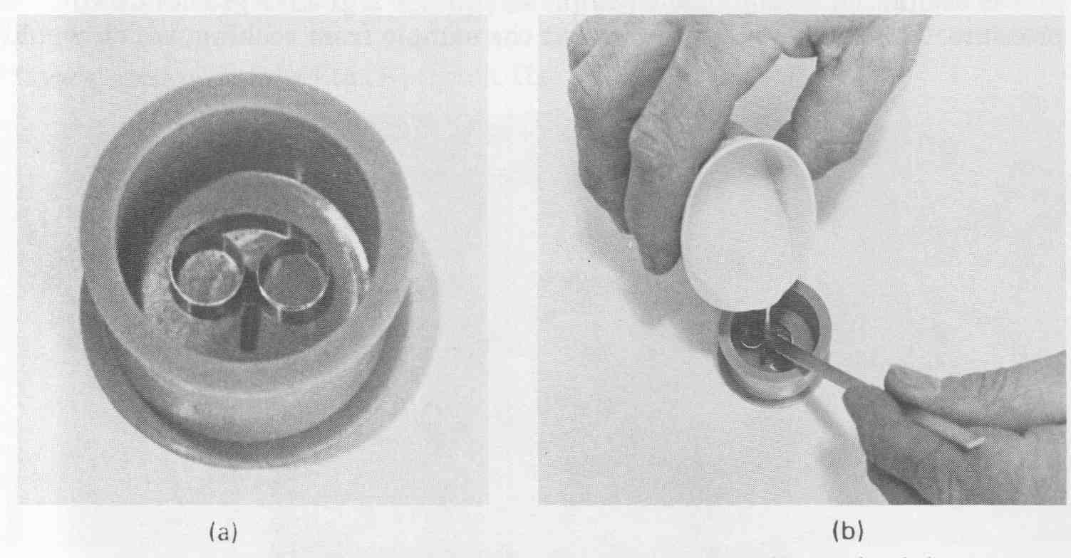
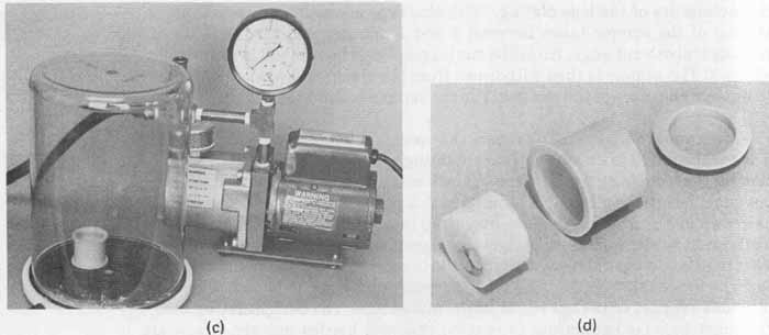
--- FIG.—16 Specimen mounting in preparation for sanding and polishing:
(a) plastic mounting ring with specimen; (b) mounting compound must cover
specimen and retaining ring; (c) vacuum pump may
be used to remove bubbles generated in the mounting compound; (d) completely
cured sample.
After the curing cycle, the sample is removed from the bell jar and from the glass. Finger pressure is applied to the plastic mounting ring to remove the sample (see FIG. 16d). The mounted sample is now ready to be sanded and polished.
Sanding and Polishing. This is a multistep operation which begins with a coarse sanding and is completed to a highly polished surface. Although sanding is often done by hand on lapping blocks (four stationary sanding blocks ranging from 240 to 600 grit), semiautomatic sanding and polishing machines, such as the one shown in FIG. 17, are widely used. When used for sanding, four different discs (240, 320, 400, and 600 grit) having adhesive backings are applied to separate wheels. Sanding begins with the 240-grit wheel being placed into the machine. The mounted sample is then placed into a retaining ring that is attached to a motor-driven arm. Steel weights totaling approximately 200 grams are placed on top of the sample to provide a good degree of downward pressure. This is necessary to prevent the sample from rocking, which would result in a nonflat surface. A small stream of water flows continuously from a nozzle to prevent overheating of the sample during the sanding operation. The machine is set at a rotating speed of 300 rpm for the 240-grit wheel. The arm to which the sample is attached moves in a back-and-forth direction as the wheel spins. This results in a figure 8 sanding pattern which duplicates that of sanding by hand. The sample is sanded on this coarse wheel for approximately 2 minutes, after which it is successively sanded on the 320-, 400-, and 600-grit wheels in an identical manner to that described. For these less coarse grits, however, the rotating speed of the wheel is increased to 600 rpm and the sample again sanded for approximately 2 minutes on each wheel. It is essential that the sample be thoroughly rinsed under cold tap water between each change of grit wheel to remove any remaining coarser grit particles from its surface.
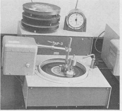
--- FIG.—17 Semiautomatic sanding unit for initial sample preparation.
After the sample has been sanded on the 600-grit wheel, it is rinsed with water and inspected for flatness. In addition, the sanded surface should display only 600-grit sanding scratches. With the sanding process completed, the sample is ready to be polished.
Polishing of the sample is done in two phases, which are (1) diamond polishing (coarse) and (2) alumina micropolishing (fine). Coarse polishing with a diamond abrasive compound will remove all scratches produced by the 600-grit sanding process and will result in extremely fine surface scratches which are barely detectable by the naked eye. Fine polishing with an alumina compound removes these minute scratches and results in an ultrasmooth surface, free of any visual blemish.
The semiautomatic machine shown in FIG. 17 is also used for polishing. Coarse polishing requires a napless polishing cloth, such as a Texmet* disk, to be initially applied to the wheel. This cloth is secured to the wheel by its self- sticking adhesive backing. A diamond paste, such as Metadi diamond compound, which has a maximum particle diameter of 1 micron (0.001 mm), is spread sparingly in a star arrangement over the polishing cloth (see FIG. 18a). The most appropriate lubricant and extender for diamond polish is a lapping oil, such as Metadi fluid. A small amount of this oil is added to the diamond paste and polishing cloth. The polishing machine is next turned on and set to a rotating speed of 250 rpm. The sample is placed in the retaining ring and weighted as described previously (see FIG. 18b). Note that water is not used in this polishing process. Satisfactory diamond polishing is completed in 2 to 4 minutes with this arrangement. With the completion of this coarse polishing process, the sample is removed from the machine and rinsed thoroughly with tap water. Contact with fingers on the polished surface should be avoided while handling the sample.
--- FIG.—18 Semiautomatic polishing: (a) application of diamond paste
to Texmet polishing cloth; (b) diamond polishing at 250 rpm.
Fine polishing requires a napped polishing cloth, such as AB Microcloth, to be applied to a second polishing wheel. This cloth also has a self-sticking adhesive backing. The diamond polishing cloth and wheel are removed from the machine and replaced with the second wheel with the napped cloth. Fine polishing is accomplished with a 0.3 micron (0.0003-mm) alumina abrasive, such as AB Alpha Polishing Alumina,* in a water slurry. A small pool, approximately the size of a half-dollar coin, of this abrasive is deposited on the polishing cloth. This alumina abrasive requires no lubricants or extenders since they are contained in the slurry. Fine polishing requires a wheel rotation speed of 600 rpm and the sample again weighted with the same weights. The final polishing process requires only approximately 1 minute to result in an ultrasmooth polished sample. After completion, it is removed from the machine and rinsed in tap water, again avoiding finger contact with the polished surface. The viewing surface appears smooth and shiny and is ready for the final step in preparing the sample for inspection.
Specimen Etching. The polishing processes cause a slight smearing of the copper and the solder platings of the microsectioned sample. In order to remove the smears so that each of these plated metals will be clearly distinguishable for inspection, a light etching is required. The liquid etch for this purpose is pre pared in a petri dish by mixing 3 parts of 26% ammonium hydroxide with 1 part of 3% hydrogen peroxide. The polished surface of the sample is immersed in this mixture for approximately 30 seconds at room temperature. The ammonium hydroxide will attack the smeared copper while the hydrogen peroxide will attack the solder to result in a microfinished sample ready for microscope inspection. The sample should be thoroughly rinsed and blow-air dried before placing it on a microscope. Finger contact with the polished surface must be avoided.
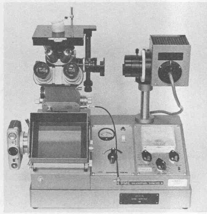
--- FIG.—19 Metallurgical inverted microscope.
Microscope Inspection. To effectively view the polished specimen, a standard inverted-type metallurgical microscope, such as the one shown in FIG. 19, is recommended. This microscope consists of (1) stage/clamp and stage adjustments, (2) eyepieces, (3) five objective lenses on a rotating nosepiece, (4) light source and internal adjustable power supply, (5) 35-mm and Polaroid cam era mount, (6) internal exposure meter, and (7) large-format viewing screen. An inverted type of microscope is recommended so that the polished surface of the sample may be placed against the stage and viewed through the objective lens located below the stage. The cross-sectional area of the hole is centrally positioned in the center of the stage and held firmly in place with a spring clip as shown in FIG. 19. For inspection of all parts of the sample, the stage may be moved left to right and front to back by vertical and horizontal stage control knobs. Concentric coarse- and fine-focusing knobs adjust the height of the stage.
The microscope can be used with minocular or binocular eye pieces with a filar. Filars are available with magnifications of 5 x, 10 x, and 15 x and are used together with the magnification of the objective lens to determine the overall viewing magnification. Objective lenses have typical magnifications of 2.5 x, 5 x, 10x, 20 x, 40 x, and 100 x. The revolving nosepiece holds five objective lenses for convenience in quickly changing magnifications. It can thus be seen that with the microscope described, magnifications can range from as low as 12.5 x (2.5 x 5) to a high of 1500 x (15 x 100).
The source of illumination is a tungsten filament lamp whose intensity is controlled by an internal power source. Filters are also available to enhance various aspects of the viewed sample. The microscope shown in FIG. 19 has pro visions for mounting 35-mm as well as Polaroid cameras and has built-in exposure and color temperature capabilities. In addition, it also has a large-f or- mat viewer which enables the magnified image to be inspected on a translucent glass plate.
Specimen Evaluation. Examination of the specimen typically begins with a low magnification, such as 50 x, in order to view the overall hole appearance and quality of fabrication. If an imperfection is detected or if a plating thickness measurement is to be taken, the sample is then viewed under a magnification of upward of 200 x.
A sample may possess a variety of characteristics or conditions which are all subject to interpretation. Because these interpretations are subjective in most cases, they should be made only by experienced personnel to determine the processing causes of observed defects. In evaluating microsections, we will discuss only those major items which are of concern to both the pc board manufacturer and the end user.
A microsection of a properly processed double-sided board is shown in FIG. 20a and that of a correctly processed multilayer board is shown in FIG. 20b. Observe the continuously smooth plated surfaces of both copper and solder with no roughness in the holes caused by drilling or the presence of foreign matter. The overall appearance should be of fine-grained copper having good registration.
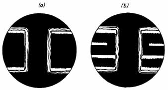
--- Fig.—20 Cross sections of plated-through holes: (a) double-sided;
(b) four-layer MLB.
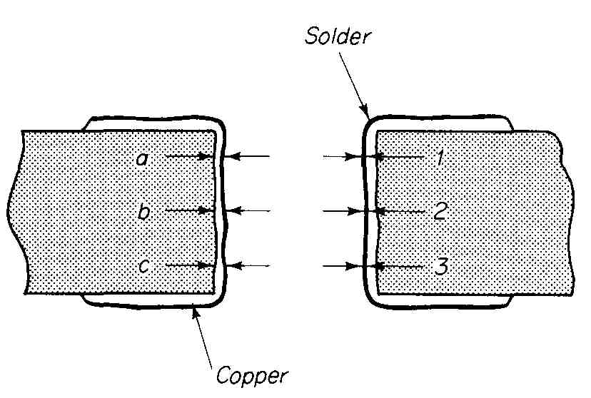
--- FIG.—21 Three measurement points to determine average plating thickness
in a PTH.
Copper and solder thickness measurements inside a plated hole should be made at a minimum of three separate locations within the hole. In FIG. 21 copper thickness measurements are taken at points a, b and c. The results for evaluation are the average of these three readings. Readings of solder plating thickness (measured before reflow) are taken at points, 1, 2, and 3 and again averaged.
Voids detected within the barrel are one of the most serious plating problems and, depending on their severity and number, may be subject to criteria for board lot rejection. A void is observed under a microscope as a break or absence in the plating that extends to the laminate base material. Such a void is shown in FIG. 22a. When a void appears it is approximately the same lateral area of the hole, such as that shown in FIG. 22b, it is called a circumferential or rim void. This defect manifests itself as a break completely around the circumference of the hole resulting in an open circuit between layers. Rim voids are always cause for board lot rejection.
Another plating problem that is detectable in microsectioning evaluation is nodulation. This is severe plating irregularities or lumps appearing within the plated hole. This defect can result in additional problems, such as plating voids, reduced plating thickness in selected areas of the barrel, and reduced hole diameter. In severe cases, nodulation is cause for lot rejection. Severe nodulation of a plated-through hole is shown in FIG.
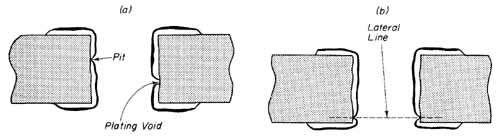
--- FIG.—22 Plating defects found in microsections: (a) plating pit
and void; (b) rim void or circumferential void.
---FIG.—23 Severe plating irregularity, termed nodulation.
--- FIG.—24 Measurements made on a microsectioned PTH.
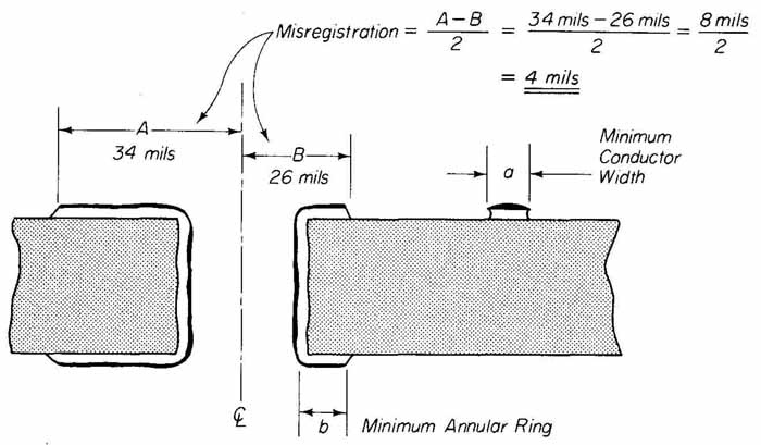
Other measurements that can be easily made on a microsectioned sample are the minimum conductor width and the annular ring (see FIG. 24). The minimum conductor width measurement is shown as dimension a. It is a determination of the amount of undercutting which resulted from the fabrication processes. The measurement of annular ring is shown in FIG. 24 as dimension b. These measurements will detect both registration and processing problems which may exist.
For multilayer boards, inner-layer registration is extremely critical and also can be determined on a microsectioned sample. A multilayer board with a severely misregistered inner layer is shown in FIG. The amount of misregistration is found by first locating the center line (CL) of the hole. Dimensions A and B are then measured from this center line. Dividing the difference between dimensions A and B by 2 will yield the amount of misregistration of the inner-layer pad.
Another defect of plated-through holes in the multilayer boards is known as epoxy smear. This is the result of excessive heat generated in the drilling process, which causes the epoxy in the laminate to melt during drill penetration. When the drill is removed, it causes the epoxy to smear over the interface area of copper and laminate. This results in an insulated area formed between the inner-layer copper and the plated barrel. Epoxy smear is detectable on the microsectioned sample and can be removed with the use of chemicals as discussed in Section 20. A multilayer board with epoxy smear on an inner layer is shown in FIG.
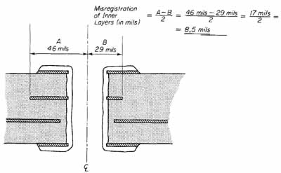
--- FIG.—25 MLB inner-layer misregistration measurement.
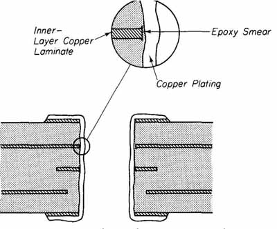
--- FIG.—26 Epoxy smear detected in microsection shows open-circuit
defect.
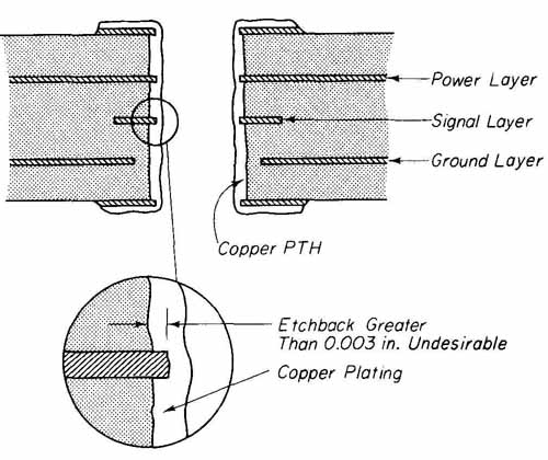
--- FIG.—27 Degree of etchback can be measured by microsectioning and
is used for process control.
Etch back is a chemical process used in the manufacture of multilayer boards. Its purpose is to remove a small amount of insulating material between inner layers before the holes are plated. This insulation removal provides a footing in order to obtain a reliable interconnection. Etchback is specified with a minimum and maximum number which ranges from 0.0002 to 0.003 inch, with typical ranges of 0.001 to 0.003 inch. If the amount of insulating material removed is insufficient, proper footing will not be achieved. On the other hand, an excessive amount removed will result in rough hole wall plating (see FIG. 27).
EXERCISES
A. Questions
1 What are the three types of tests required to completely inspect a pc board?
2 What is the magnification of a 5-diopter lens?
3 What type of equipment should be used to measure the width of a gold- plated finger?
4 Define the defect termed rim void and explain why it is unacceptable.
5 What caution should be exercised when using pin gauges to measure the diameters of plated-through holes?
6 Explain the difference between dedicated and universal bare-board testers.
7 What is the best type of equipment to use in measuring the plating thickness of a PTH?
8 List in order the six basic steps required to prepare and inspect a sample PTH microsection for evaluation.
9 Discuss the advantages and disadvantages of taking a sample PTH from the thief area compared to that taken from the imaged area.
10 What is the recommended method of removing a sample PTH from a board without damage in preparation for microsectioning?
11 Describe the procedure for specimen mounting.
12 List four major defects that are detectable through microsection evaluation.
13 What are the two types of surface defects that are readily visible under a magnifying lamp?
14 List three examples of circuit bridges.
15 What three common circuit pattern features can be measured with a comparator?
16 Describe a simple procedure for determining if an internal short circuit exists between power and ground planes of a MLB.
17 With reference to FIG. 25, calculate the inner-layer misregistration if dimension A is 50 mils and dimension B is 40 mils. Is this acceptable if the maximum allowable misregistration is 6 mils?
True or False
Circle T if the statement is true, or F if any part of the statement is false.
1 As the lens power in diopters increases, the object distance from the lens decreases. T F
2 A 10 x comparator is used primarily to detect flaws in etched conductor patterns. T F
3 Plating voids are acceptable if many of them appear in one processed hole. T F
4 A tapered-pin hole gauge is used to accurately measure a plated hole. T F
5 A universal test head has probes positioned on grids spaced at 0.1-inch intercepts. T F
6 The Caviderm nondestructively tests the plating thickness of a plated-through hole. T F
7 Test coupons used for microsectioning are located inside the corner brackets of a pc board. T F
8 Microsectioned samples receive a final polishing phase using a 0.3-micron alumina abrasive. T F
9 A magnification of 600 x is obtained when using a 15 x filar with a 40 x objective lens. T F
10 An etchback greater than 0.003 inch is required to result in proper footing of a PTH. T F
C. Multiple Choice
Circle the correct answer for each statement.
1 (Destructive, nondestructive) testing is necessary to accurately deter mine the manufacturing quality of a pc board.
2 The most accurate annular ring measurements are made with a (comparator, dial indicating caliper).
3 Hole diameters on pattern-plated pc boards are more accurately measured with a (tapered pin, plug gauge).
4 Microsectioning is a (destructive, nondestructive) test procedure.
5 Bare-board testing of pc boards is intended for (prototype, volume) production.
6 A nondestructive test for measuring copper plating thickness is with the use of a (Caviderm, bare-board) tester.
7 The detection of epoxy smear requires the use of (a Caviderm, micro- sectioning).
D. Matching Columns
Match each item in column A to the most appropriate item in column B.
COLUMN A | COLUMN B
1. Microsectioning 2. Comparator 3. Caviderm 4. Plug guage 5. Etchback 6. Bare-board tester |
a. Detected in microsection b. Bed of nails c. 10 x magnifer d. Plating thickness measurement e. Destructive testing f. Hole diameter. |