AMAZON multi-meters discounts AMAZON oscilloscope discounts
0. INTRODUCTION
The projects presented in this section have been selected to allow students to practice the skills discussed in this book. These projects illustrate varying degrees of construction complexity. While the cost of constructing these projects was a consideration, primary emphasis was placed on the application of current technology as well as their usefulness.
The authors are aware of the necessity to substitute parts and devices because of availability considerations. Many devices and components are not critical, and where indicated, equivalencies may be substituted. For this reason, and also to familiarize the student further with the selected circuit, it is strongly recommended that the circuit be breadboarded and tested before fabrication. This approach also provides an opportunity for the advanced student to modify a project.
The presentation of each project begins with a general discussion of the circuit operation to acquaint the student with its function. This is followed by a circuit schematic and a complete parts list. Finally, construction hints are provided to avoid packaging difficulties.
The finished packages shown pictorially are to be considered as typical. The student, of course, is not restricted to the design shown and should feel free to employ ingenuity in fabricating a package that will reflect his or her own requirements and desires.
The following projects are presented in this section:
• Darkroom Timer
• TTL Logic Probe
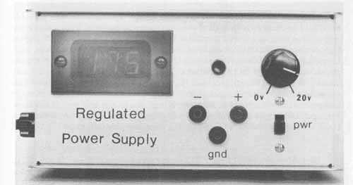
• 1.2- to 20-Volt Laboratory Power Supply with Digital Readout
• Portable Fahrenheit/Celsius Thermometer with LCD Readout
• Sportsman’s Barometer with LCD Readout
• Automobile Security Alarm System
As an aid in construction, pin configurations for all of the devices used in these projects are provided in FIG. 1.
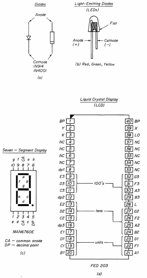
--- FIG.—1 Device configurations for projects: (a) diodes; (b) light-emit
ting diodes (LED5): red, green, yellow; (c) seven-segment display, CA—
common anode, DP—decimal point; (d) liquid crystal display (LCD); (b)
Red, Green, Yellow
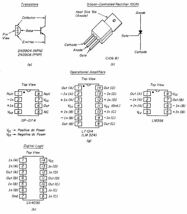
--- FIG.—1 (Cont.) (e) transistors; (f) silicon-controlled rectifier
(SCR); (g) operational amplifiers; (h) digital logic; Heat Sink Tab (A
node)
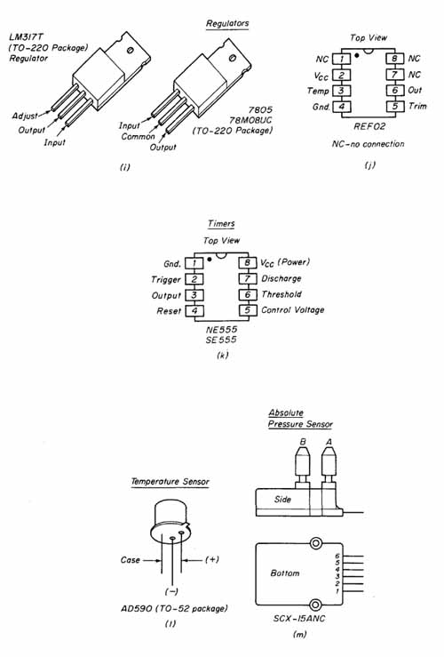
--- FIG.—1 (Cont.) (I) regulator; (j) regulator; (k) timer; (I) temperature
sensor; (m) absolute pressure sensor;
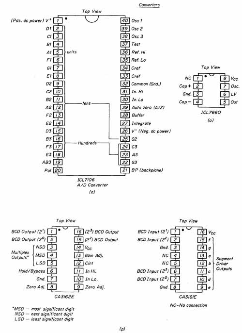
--- FIG.—1 (Cont.) (n—p) converters.
1. DARKROOM TIMER
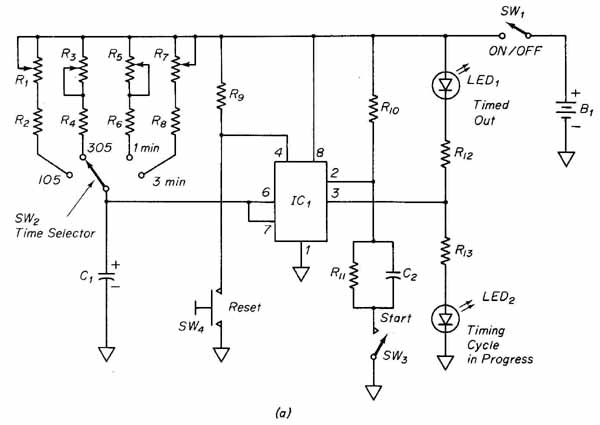
This darkroom timer circuit employs the popular 555 timer IC, which is readily available from electronic parts suppliers. The timer features four fixed time- delay intervals, a timing cycle in progress indicator, a timed-out indicator, and separate start and reset controls. Although this timer circuit was designed to aid in photographic film developing, it is sufficiently flexible to be adapted to many purposes where a portable timer is necessary.
Circuit Operation. Power is applied to the timer circuit shown in FIG. 2, by closing switch SW The voltage at pin 3 of IC is at approximately 0 volts. This forces the timing cycle in progress indicator LED off and the timed-out indicator LED to be on. One of four time delays can be selected with the time- selector switch SW The time delay is set by C and the two-resistor combinations functioning with SW The timer shown in FIG. 2 is designed for delays of 10 seconds, 30 seconds, 1 minute, and 3 minutes. Potentiometers R1, R3, R5 and R7 are used to adjust the individual time delays. A description on setting these potentiometers for the desired delays is given in the circuit calibration section.
Momentarily depressing the start switch SW forces pin 2 of IC to about 0 volts and begins the selected time delay. Pin 3 goes to a positive voltage, lighting LED and shutting off LED At the completion of the delay time, pin 3 returns to about 0 volts, turning on LED (timed-out indicator) and shutting off LED (timing cycle in progress).
Normally, R holds pin 4 of IC high at about 9 volts. If, however, the reset switch SW is depressed during a timing cycle, pin 3 of IC will go immediately to about 0 volts, which activates LED and cancels the cycle. A new delay time cycle can then be initiated with the start switch SW It is important that the timing capacitor C have a good-quality tantalum or polystyrene dielectric.
--- FIG.—2 Circuit schematic for the darkroom timer.
--- FIG.—2 (Cont.)
Circuit Calibration. The time delays for the circuit of FIG. 2 are calculated using the relationship T 1.1RC1 where T is in seconds, C1 is in farads, and R is the two-resistor combination (R1 + R2) or (R3 + R4) or (R5 + R6) or (R7 + R8) in ohms, determined by the position of the time selector switch SW2.
The setting of a 10-second time delay will be used to demonstrate the calibration of the circuit. Resistor R1 is first adjusted to one end of its range. The circuit is cycled and the delay timed. R is then adjusted to the other end of its range and again the cycle is timed. These two readings will provide the range of the time delays possible for the two-resistor combination of R and R. To obtain an exact 10-second delay time, R is adjusted within the range and the time cycle recorded. This fine tuning is repeated until the exact 10-second delay results. To set and fine tune for the other three time-delay periods, the calibration procedure described is repeated for each position of the selector switch SW2.
Construction Hints. There are no special construction problems with this project. As shown in FIG. 3, a suggested package is a small, commonly avail able chassis. Note that LED and LED are positioned to be prominently visible. Since the start and reset switches will require extensive use, SW is positioned on the top and SW on the front face of the package. The power switch SW is placed along the side.
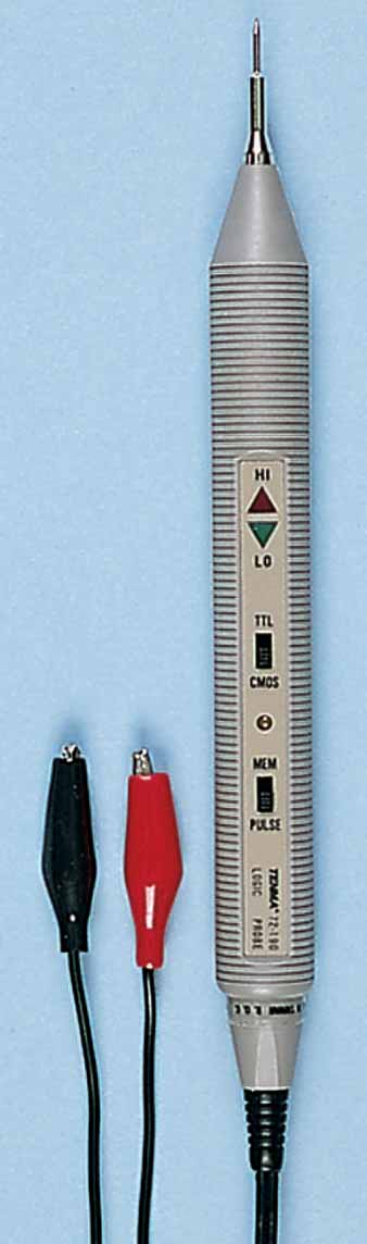
2. TTL LOGIC PROBE
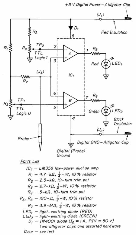
Digital circuitry plays a major role in today’s electronics industry. While new families of devices are introduced to keep up with the demands of changing technology, TTL (transistor-transistor-logic) devices maintain their dominance due in part to their ready availability and simplicity of use. A technician working with and troubleshooting digital circuits using these devices finds a time saving instrument in a TTL logic probe. The probe described in this project uses readily available parts, is easy to build, and provides effective results.
Circuit Operation. The TTL logic probe shown in FIG. 4 is designed around a LM358 low-power dual op amp capable of single-supply operation. Power for the probe is applied when the red alligator clip, connected to J is attached to the + 5-volt power supply bus of the digital circuit to be tested. The probe ground is made when the black alligator clip, connected to J is attached to the digital circuit’s ground bus. The purpose of diode D is to prevent dam age to the probe circuitry if these power supply connections are inadvertently reversed.
With power applied, the probe is calibrated as follows: The positive lead of a dc voltmeter is connected to test point 1 (TP and the negative lead to J Potentiometer R is adjusted until a reading of exactly 0.8 volt appears at TP This is the maximum allowable voltage level for a TTL logic 0. The positive lead of the voltmeter is next connected to test point 2 (TP and potentiometer R is adjusted for a voltage reading of 2.0 volts, which is the minimum allowable TTL logic 1 level.
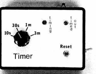
--- FIG.—3 Suggested package for the darkroom timer.
--- FIG.—4 TTL logic probe schematic.
The circuit can be tested by first contacting the probe to a known logic 0 (or to digital ground). The output of op amp B at pin 7 will go to about + 3.0 volts and the green light-emitting diode (LED will light to indicate a logic 0 state. The red diode (LED will remain off. The probe is next contacted to a known logic 1 (or to the digital power supply’s + 5-volt bus). This will cause the output of op amp A to go to about + 3.0 volts, lighting LED which indicates a logic 1 level. Resistors R and R limit the LED “on” current to about 10 mA to conserve power.
The purpose of R is to maintain the probe voltage above 0.8 volt and below 2.0 volts, which is called the “forbidden” area for TTL logic. Thus, when the probe contacts neither the logic 0 nor logic 1 state, both of the LEDs will be off.
Construction Hints. Construction of the TTL logic probe requires no special considerations. Fabrication of a pc board is recommended but is not essential. The probe package shown in FIG. 5 was constructed using a modified probe case. The sharp metal probe is isolated from the case and wired to terminal J on the pc board with a short length of hook-up wire.
Power (red) and ground (black) leads are AWG No. 24 stranded wire fitted with miniature alligator clips and extend into the probe case. All probe circuitry shown with the digital ground symbol $ must be electrically connected together and to the black external ground lead J.
A final consideration in the packaging of the probe is in the composition of the case. If it is metal, care must be exercised to ensure that none of the circuitry touches it electrically. Any type of round hollow material, such as a short length of PCV piping or a hard plastic tube, may be used as the probe case.
3. 1.2- to 20-VOLT LABORATORY POWER SUPPLY WITH DIGITAL READOUT
One of the most useful projects the experimenter can construct is a laboratory- type dc power supply. Applications of this type of circuit are almost unlimited. However, for a power supply to be most useful, it should have the following features: (1) adjustable output-voltage capability over a wide range, (2) high- load-current capability, (3) excellent voltage regulation at all load currents, (4) current limiting with short-circuit protection to prevent damage to the supply when accidental overloads or shorts are applied to the output terminals, and (5) metering to monitor output voltage.
The variable-voltage-regulated power supply circuit, shown in FIG. 6, will meet all of the foregoing requirements with the following specifications:
Output voltage: adjustable from 1.2 to 20 volts dc
Output current: 0 to 1 ampere
Voltage regulation: 0.1%
Including: Load-current limiting
Thermal-overload protection
Safe-area-device protection
---FIG.—5 TTL logic probe package.
The requirements listed for a basic laboratory-type power supply are easily met with the use of an integrated regulator chip having only three external terminals: input (in), output (out), and adjustment (adj). These are shown in FIG. 6. The resulting circuit is (1) low in overall parts count, (2) inexpensive, and (3) simpler to package than a comparable-type discrete power supply.
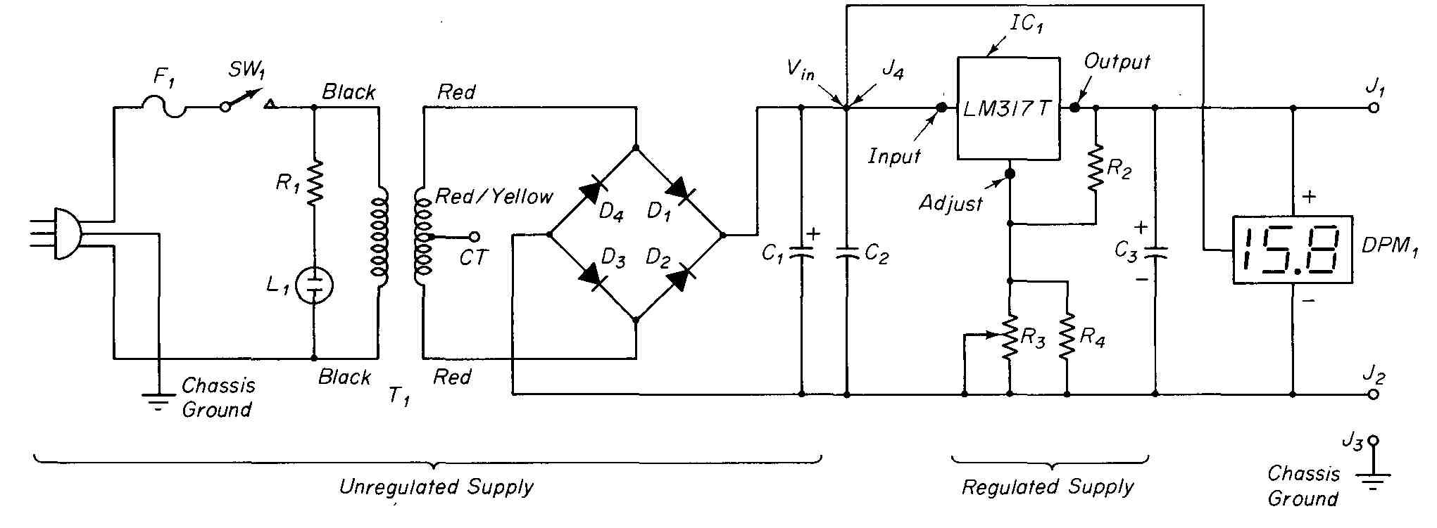
--- FIG.—6 Schematic diagram of variable-voltage-regulated power supply.
Circuit Operation. For purposes of analysis, the power supply circuit schematic diagram, shown in FIG. 6, can be divided into two basic sections: an unregulated power supply and a voltage regulator section. The unregulated power supply consists of transformer T diodes D to D in a full-wave bridge configuration, and the filter capacitor C
The basic regulator section consists of the LM317T regulator chip and support components R2, R3, R4 C2 and C3.
The LM317T regulator chip requires that the output of the unregulated supply, across filter capacitor C1 be limited to a maximum of 40 volts dc. This specification is easily met by T since its theoretical peak output voltage under no-load current conditions is approximately 34.5 volts dc. Under full-load cur rent conditions of 1 ampere, the dc output voltage of the unregulated supply is approximately 27 volts dc.
All of the electronics necessary to produce an adjustable, positive regulated power supply are contained in one three-terminal integrated circuit pack age, available in several standard package styles. The TO-220 plastic case was selected for this project. An internal reference voltage of 1.2 volts (constant) is established between the output (out) and the adjustment (adj) terminals of the LM317T regulator. This reference voltage is applied directly across the 240-ohm resistor (R establishing a constant reference current of 5 mA flowing through R This reference current also flows through the potentiometer (R and parallel padding resistor R). An increase in the resistance of R results in larger output voltages while a decrease in R results in lower voltages. The minimum dc output voltage can never be lower than the reference voltage of 1.2 volts.
An ac ripple voltage is present on the input terminal of the regulator chip. At full-load currents of 1 ampere, this ripple can be as high as 5 volts peak to peak. On the output terminal of the regulator, there is essentially no ripple voltage (5 mv or less). The ripple voltage that is present at the input terminal is absorbed by the regulator.
Capacitor C is a 0.1-uF disc required if the lead length from the unregulated supply terminal is excessive (2 inches or longer). It is, however, good practice to always include this capacitor. Capacitor C (10-uf tantalum) is connected from the output terminal of the regulator to common to improve the transient response of the regulator.
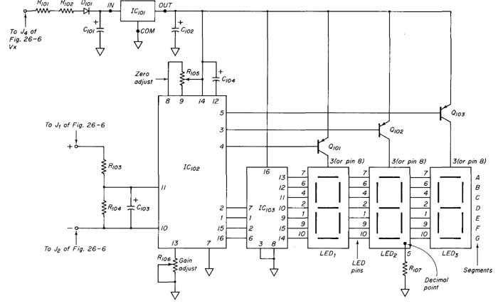
Fig. 7 Schematic diagram of the digital panel meter readout for the regulated power supply project.
The dc output voltage appearing between terminals J and J is monitored with a digital panel meter (DPM), which will next be described in detail.
Digital Panel Meter. Recent advances in the development of integrated circuit technology have made it possible to replace older, less reliable analog panel meters with digital readout at lower costs and moderate increases in circuit complexity. To illustrate this, the power supply described in this project will be provided with a digital panel meter instead of the traditional analog meter. This DPM is designed around two 16-pin dual-in-line packaged ICs and support components as shown in FIG. 7. The core of this DPM system is the RCA CA3162E integrating analog-to-digital (AID) converter and its companion, the CA3161E BCD-to-seven segment decoder/driver IC.
DC power for the DPM is provided from the unregulated output section at J of FIG. 6. This voltage (Vm) is then converted by IC (FIG. 7) to + 5.0 volts.
The output voltage of the power supply to be monitored is between J and J of FIG. 6. This voltage is connected between the + and — input of the DPM (see FIG. 7). The voltage is divided by R and R and feeds into the A/D converter (IC which converts the analog voltage into a binary-coded decimal (BCD) equivalent that appears at pins 2, 1, 15, and 16. IC102, in turn, takes this BCD code and converts it into a seven-line output that represents a decimal number. These seven-segment outputs are multiplexed to LED1, LED2 and LED3 The digits are selected by pins 3, 4, and 5 of IC which provide base drive to turn on Q101, Q102 or Q103 These transistors then feed cur rent to the anodes of the appropriate LED readouts.
--- FIG.—8 Printed circuit board assembly to the digital panel meter (DPM) section
of the power supply project.
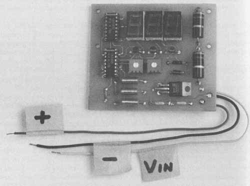
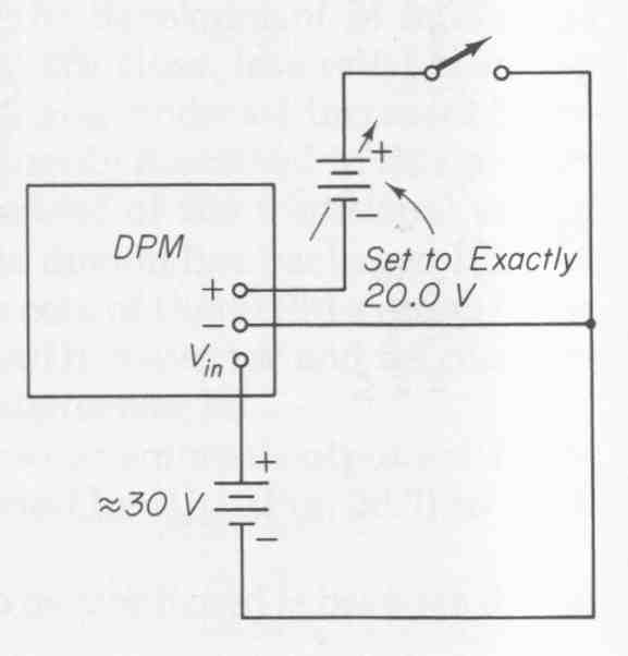
The DPM assembled on a double-sided pc board is shown in FIG. 8. The DPM requires calibration prior to being integrated into the power supply project. This is done with the calibration setup shown in FIG. 9. A power supply of approximately 30 volts is connected between Vm and — of the DPM. To zero the meter, the + and — inputs are shorted and R is adjusted for an output reading of 00.0. To calibrate the meter, the short is removed and a precise voltage, for example 20 volts, is applied between the + and — inputs. Potentiometer R is then adjusted for a reading of exactly 20.0 on the DPM.
--- FIG.—9 Calibration setup for the digital panel meter.
--- FIG.—10 Assembly diagram of LM317 regulator package to chassis.
--- FIG.—11 Basic package configuration for the power supply project.
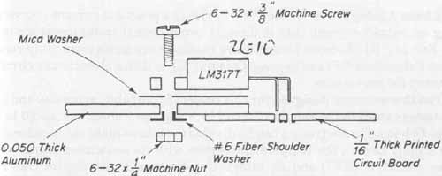
Construction Hints. For optimum performance, the power supply circuit should be packaged in a well-ventilated enclosure. The LM317T regulator pack age will require heat sinking to achieve the required specifications. A metal chassis element can be used as a suitable heat sink provided that it consists of at least 25 square inches of aluminum. The regulator chip must be electrically insulated from the chassis. This is done with the use of a silicon- greased mica washer and insulating shoulder washer (FIG. 10). Note that the leads are bent at 90 degrees onto a pc board. The pc board is used to assemble all the small fragile circuit components. A three-pronged plug is essential for electrical grounding of the chassis. The basic power supply package is shown in FIG. 11.
4. PORTABLE FAHRENHEIT/CELSIUS THERMOMETER WITH LCD READOUT
The accurate measurement of temperature requires a sensor that is linear and its readings repeatable. To satisfy both of these requirements, this electronic thermometer project is designed around the popular AD590 linear integrated circuit from Analog Devices, Inc. This device is a practical current source producing an output current that is directly proportional to temperature in degrees Kelvin (°K). Because temperature readings are more commonly read in degrees Fahrenheit (°F) and degrees Celsius (°C), additional electronic circuitry is required for conversion.
The thermometer designed for this project is portable, accurate, and measures temperature in the ranges of 0 to 199.9 degrees Fahrenheit and 0 to 100 degrees Celsius. Its electronics can be divided into three main subdivisions: the power supply circuit, the temperature sensor with its associated signal-conditioning circuitry (SCC), and an integrating-type analog-to-digital converter (AD C) with its liquid crystal display (LCD) readout. Each of those circuits will be described in detail.
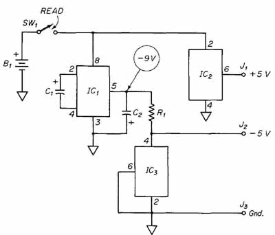
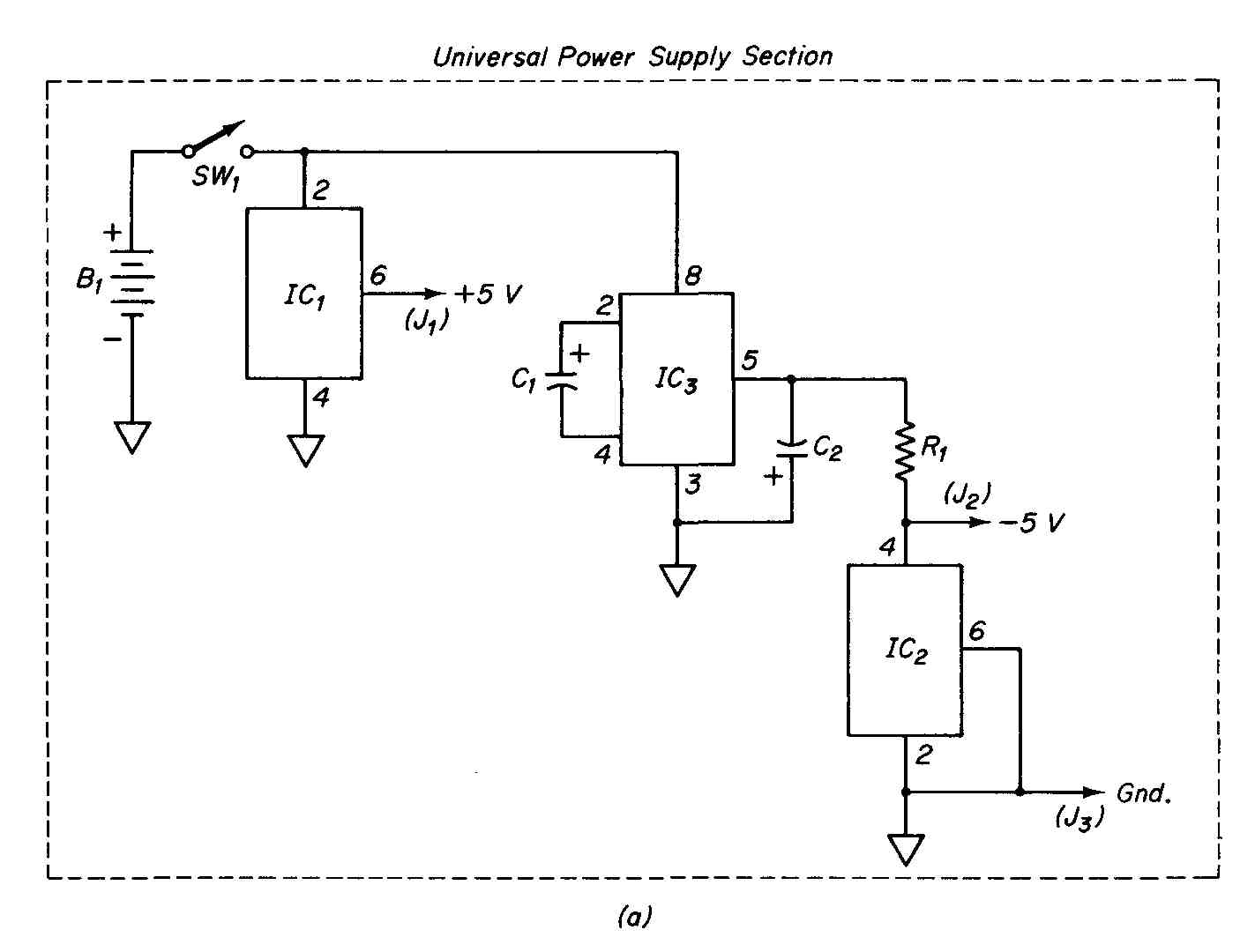
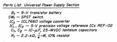
Universal Power Supply. A common design specification for portable hand-held equipment is that all of the electronics be powered from a single energy source such as a 9-volt transistor battery. While standard CMOS digital logic can operate at this voltage level, much of the current analog devices, such as operational amplifiers, require split (dual) voltage sources. The power supply circuit shown in FIG. 12 provides a regulated ±5-volt source from a 9-volt battery. When SW (READ) is closed, IC converts the + 9-volt battery level into a precise + 5.000 volts reference at pin 6 of IC This reference at J is thus made independent of reductions in battery voltage due to age and use. A negative nonregulated output of -9 volts is then developed with IC and two noncritical 10- tantalum capacitors C and C IC regulates this output to —5 volts at J.
Signal-Conditioning Circuit. The power supply circuit shown in FIG. 12 provides a precise + 5-volt reference for both the AD 590 temperature sensor and its associated bridge circuitry. This is shown in FIG. 13. Resistor R converts the sensor’s temperature-dependent current into a temperature-de pendent voltage that is applied to the + input of the instrumentation amplifier (IA). The — input of the IA is returned to the null (zero offset) circuitry of the bridge reference through the scale selector switch SW When SW is down, the offset voltage at TP is applied to the IA to zero the Fahrenheit scale. When SW is up, the voltage at TP is returned to the — input of the IA to zero the Celsius scale. The three-op amp IA, consisting of IC A, B, and C and its associated circuitry, performs two major functions. First, it provides a single-ended output voltage to drive the input of the ADC voltmeter and second, it applies the correct amplification so that the output voltage of TP is scaled to (10 mV/°F) TF or (10 mV/°C) T depending on the position of SW2.
---FIG.—12 Power supply electronics to develop ±5 volts for the thermometer
project.
--- FIG.—13 Sensor and signal conditioning circuitry (SCC) for the thermometer
project.
Circuit Calibration—Fahrenheit Scale. With power supply switch SW closed and SW down (°F position), a digital voltmeter is connected between TP and circuit ground. At room temperature of approximately 77.5°F, the voltage across R should be about 293 mV. By pinching the AD590 sensor between the index finger and thumb, the body temperature will increase this voltage at TP by about 7 mV for a reading in the vicinity of 300 mV. With this basic test completed, the calibration procedure continues. The offset adjustment is made by connecting a digital multimeter (DMM) to TP and adjusting R for a voltage reading of precisely 255.4 mV. Span adjustment (or gain adjustment) requires that the DMM be connected to read the voltage of TP The room temperature is then measured, in °F, with a high-quality laboratory thermometer, and the output voltage reading at TP corresponding with this temperature is calculated using the relationship V = (10 mV/°F) TF. For example, if the room temperature measures 77.5°F, then V = (10 mV/°F) 77.5°F = 77.5 mV. For this example, R would be adjusted for a reading at TP of 775 mv. With a fixed decimal point positioned between the 7 and the 5, the digital volt meter would provide a direct reading in °F (i.e., 77.5).
Circuit Calibration—Celsius Scale. The offset adjustment is made by first placing SW in the up position for the °C scale. A DMM is then connected to TP and R is adjusted for a voltage reading of exactly 273.2 mV. (No span adjustment is required on the Celsius scale.) the DMM is moved to TP and again, room temperature is precisely measured in °C. The corresponding voltage reading of TP for the temperature is calculated with the equation V = (10 mV/°C) T For example, if the room temperature is 24.5°C, then V = (10 mV/°C) 24.5°C = 245 mV, which corresponds to 24.5°C.
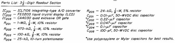
Circuit Description—3-Digital Readout System. The readout system for the thermometer project is built around the familiar 1CL7106 dual-slope integrating-type AID converter and a 0.6-inch high-character LCD (see FIG. 14). Both the ADC and the LCD are housed in 40-pin dual-in-line packages. The supporting components have been selected to optimize circuit performance for a 0- to 199.9-mV full-scale input range and a corresponding output display.
Output signals from the SCC and TP of FIG. 13 are applied to the A/D converter through a low-pass filter (R and C having a cutoff frequency of approximately 15.9 Hz. The input signals that are passed are processed by the dual-slope method of conversion employed by the 7106 IC. This conversion method samples input voltage and converts it into a current that charges capacitor C for a fixed interval. At the end of this charging time interval, the input signal is replaced by a precise reference voltage which is developed across C and established externally by adjusting R. This reference voltage allows C to be discharged at a constant rate until its charge is completely removed. The time for this discharge is therefore directly proportional to the value of the input voltage level and is measured with an internal counter operating from an internal clock.
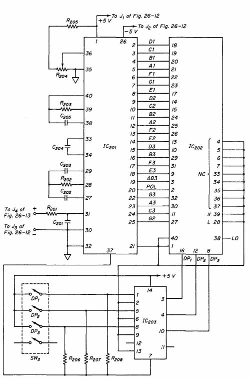
--- FIG.—14 Circuit schematic of the 1CL7106 A/D converter and LCD readout.
--- FIG.—15 Portable Fahrenheit/Celsius thermometer with liquid crystal
display: (a) major PCB assemblies; (b) completed project.
To test that the internal clock is operating correctly, an oscilloscope (or counter) is connected between pins 37 and 32 (GND) of IC201. With a 10 x probe, a clock frequency of 48 kHz ±20% is an acceptable reading.
All digital decoding and drive necessary to interface to a low-power LCD is provided on the 7106 IC. The decimal-point position for the LCD is selected by depressing one of the three switches labeled dp on SW3 For this project, dp should be the choice so that the output of the SCC will be interpreted directly into units of °F or °C.
As a final note, it is recommended that capacitors C202, C203 and C204 be manufactured with a polypropylene or Mylar dielectric.
Final Circuit Calibration. To complete the final calibration of the digital readout system, a DMM is connected between pins 36 and 32 (GND). Potentiometer R is adjusted until an exact reading of 100.0 mV is obtained. The system is then ready to accept the input signals from the SCC circuit.
Construction Hints. The electronic thermometer shown in FIG. 15 is housed in a readily available plastic instrument box. All of the signal-conditioning circuitry was assembled on a 2- by 3-inch single-sided pc board that is piggybacked with a 3-by 5-inch double-sided board on which is packaged the ADC and LCD display. The universal power supply circuit is assembled on a 1- by 2-inch pc board. The AD 590 temperature sensor, soldered to a 3-foot length of twisted pair AWG No. 24 wire, is external to the chassis as shown in FIG. 15a.
To complete the package, a 1- by 2-inch cutout was formed in the plastic case to expose the LCD. A small DPDT switch (SW the scale selector switch) is mounted on the front of the case and labeled. Last, the pushbutton SPST switch (SW is also mounted on the case front. Depressing this button applies power and displays the temperature. Upon releasing the button, power is re moved in order to conserve battery life. These are shown on the completed thermometer package in FIG. 15b.
5. PORTABLE SPORTMAN’S BAROMETER WITH LCD READOUT
The sportsman’s barometer project, shown in FIG. 16, is built around a solid- state absolute pressure sensor (type SCX15ANC from Sensym Corporation). The rugged construction of this sensor provides high reliability at moderate cost.
A portable barometer has significant advantages to those who spend a great deal of time outdoors hiking, skiing, fishing, and so on, where changing weather conditions may alter one’s plans suddenly. A drop in barometeric pres sure signifies stormy weather is approaching while a rising pressure indicates fair-weather conditions ahead. A steady pressure denotes unchanging weather patterns.
This portable barometer outputs absolute pressure digitally in units of inches of mercury (in. Hg) in a range from 28.0 to 32.0 in. Hg. As an aside, fishermen have found that the best fishing occurs when sea-level pressure is between 29.6 and 30.4 in. Hg and rising.
Note in FIG. 16 that both the universal power supply section and the 3 -digit readout sections are similar to those described in the section on the thermometer project. They are shown here for purposes of completeness, but their operation will not be repeated.
Circuit Operation—Pressure Sensor and Signal-Conditioning Circuit. Pres sure sensor PS100 outputs a differential voltage between pins 5 and 3 that is directly proportional to absolute pressure. This voltage is applied to the instrumentation amplifier consisting of IC IC and resistors R R R R and R R is a precision 1% 3.24-ku resistor which sets the IA’s gain and scales the output at pin 6 of IC into units of in. Hg. The output voltage of IC is applied to the readout section for the digital display. Dc power for the three op amps as well as for the sensor is obtained from the universal power supply.
Circuit Calibration. Prior to calibrating the sensor SCC, the reference voltage for the digital readout section should be adjusted just as it was in the thermometer project. A DMM is connected between pins 36 and 32 (GND) and R is adjusted for an exact dc voltage reading of 1.00 volt. The readout section is now ready to accept input signals. To calibrate the barometer, it is first necessary to obtain the barometric pressure by calling the local airport or weather station. Closing SW to apply power to the system, R is adjusted until the digital readout displays the correct pressure.
--- FIG.—16 Complete circuit schematic and parts list (or the sportsman’s
barometer project: (a) universal supply section;

--- FIG.—16 (Cont.) (b) pressure sensor and signal conditioning circuit
section.
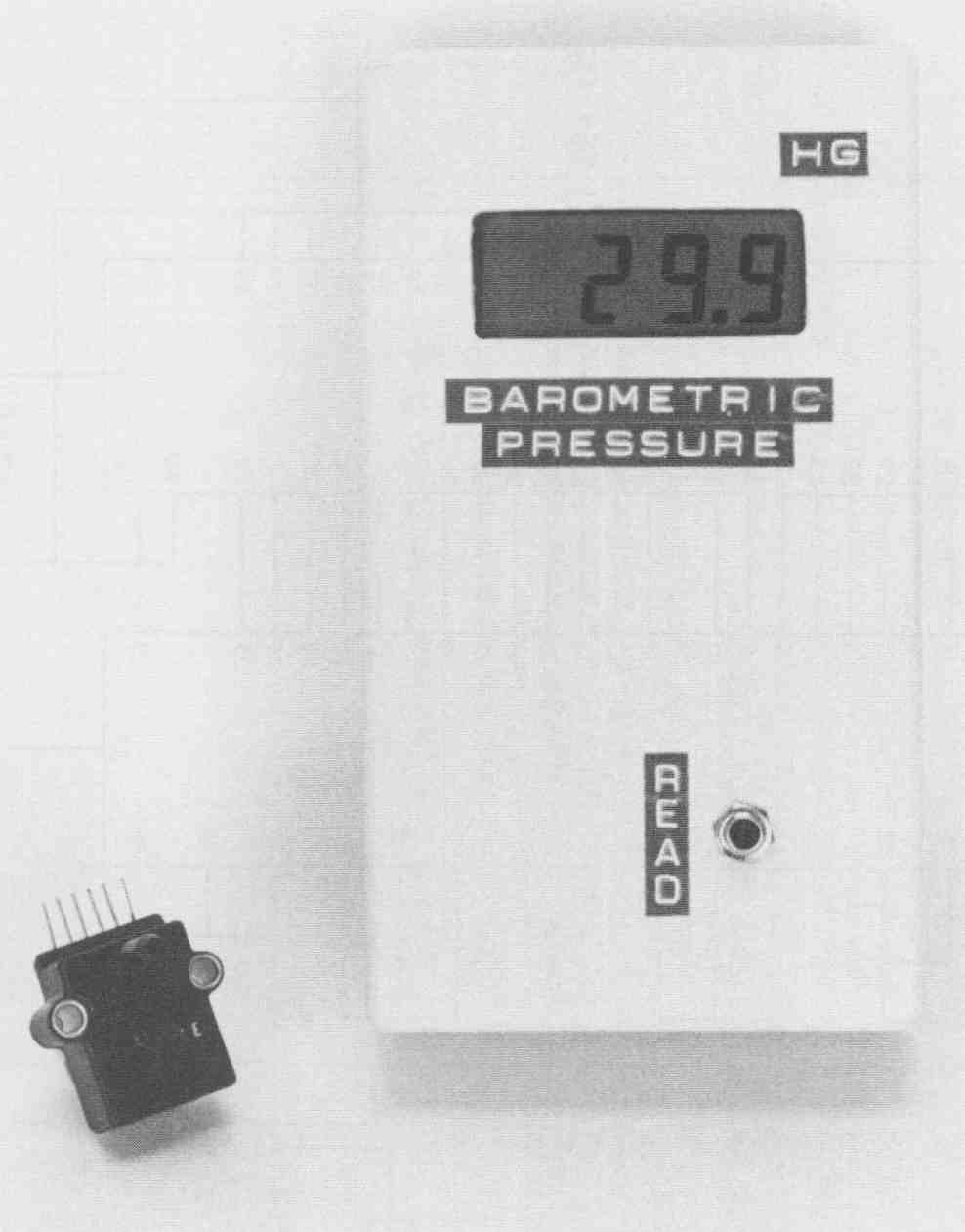
--- FIG.—17 Sportsman’s barometer.
Construction Hints. The completed sportsman’s barometer project is shown in FIG. 17. Note that it is packaged in the same type of plastic case as the previous project on the thermometer. For this reason, all of the construction hints presented in that section also apply to this project.
6. AUTOMOBILE SECURITY ALARM SYSTEM
Although no alarm system is foolproof, they do serve as a deterrent to automobile thefts, especially those thefts committed by the amateur. The most positive types of automobile alarm systems are those which employ mechanical door, hood, and trunk switches. Although this type of system is more difficult to install than the voltage- or current-sensing type of alarm systems, it is less susceptible to false triggering due to climate changes, extreme variations in temperature, or outside electrical interference. The most effective alarm systems are those that are completely concealed inside the automobile, thus giving potential thieves a false sense of security. The automobile security alarm system, shown in FIG. 18, is a reliable, relatively inexpensive system that will provide a high degree of security for an automobile.
Circuit Operation. An automobile security alarm system is usually in stalled in the trunk of the automobile. All the required electrical connections are then made from this location.
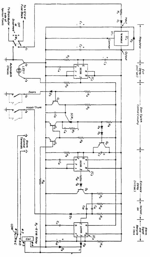
--- FIG.—18 Circuit schematic for the automobile security alarm system.
Switch SW is a DPDT slide or toggle switch that serves two functions: it “arms” or “disarms” the alarm system. In the “armed” position, the switch acts to connect the distributor side of the ignition points to ground, thus pre venting the car from being started. This arm/disarm switch is usually mounted under the dashboard of the car, hidden from view but accessible to the driver.
The alarm system includes (1) an exit delay, (2) an entrance delay, (3) alarm and recycle, and (4) an “instant on” protection feature for both the hood and trunk. To activate the system, the arm/disarm switch SW is moved from the “off” or “disarmed” position to the “armed” position. After the switch has been activated, the operator has a preset exit delay time of approximately 17 seconds to leave the car and lock the doors. (If closing the doors takes longer than 17 seconds, the horn will sound.) The exit delay time interval is set by the timing capacitor C and resistor R. At the end of the exit delay cycle, the out put of IC at pin 3, goes from approximately 0 volts to 6 volts, applying power to the reset terminals of IC and IC at pin 4. The system is now armed and ready to detect an intruder entering any protected door. If desired, LED can be connected between jacks J and J as shown in FIG. 18. LED will light at the end of the 17-second exit delay interval, indicating that the system is armed. This light can be mounted on the dashboard of the car.
Once the circuit is armed, the door switch control circuitry, consisting of R R Q D SCR R D D Q arid Q is also powered. As long as all door switches are open (door switches are open when car doors are closed since the door position depresses the switch plunger), transistor Q remains on and acts as a short circuit across C preventing IC from operating. An intruder opening a door causes the switch plunger to release and closes the switch, which causes the collector of Q to go high, firing the gate of SCR The base of Q will go to approximately 0 volts, causing its collector-to-emitter to act as an open circuit across C The timing capacitor C (associated with IC begins to charge). The intruder now has 11 seconds to find the arm/disarm switch and return it to the “off” position. If the switch is not thrown within the preset entrance delay time of ii seconds, the charge developed across C (through resistor R will cause the output of IC (pin 3) to go high, thus triggering IC With IC triggered, its pin 3 goes high, turning on diode D which places 6 volts across the coil of the relay, Ry. The relay switches from its normally open condition to cause a closed condition at points J and J As can be seen in FIG. 19a, b, or c, when J and J are shorted together by the switching action of relay Ry, they complete the alarm circuit. This causes the alarm siren or automobile horn to sound for a duration of approximately 1 minute, this time interval being set by R and C After the alarm sounds for 1 minute, the system will recycle. If, for example, during the 1-minute sound interval, the intruder is frightened off and closes the door which he initially opened, the system will recycle. Even though the door has been returned to its closed position, the sound will complete its 1-minute cycle, after which the system is set and ready to detect another door intrusion. If, on the other hand, the intruder leaves without closing the door which he initially opened, the alarm will sound for 1 minute, shut down for an 11-second interval, and then sound again for 1 minute. This 1 minute on/il seconds off cycle will continue until the opened door is finally closed.
Since it is not advisable to have any delay on either the hood or trunk switches, the “instant-on” feature accomplished by C R and D is included. Opening either the hood or trunk after the system has been armed will instantly sound the alarm for the same preset 1-minute interval as established by R and C
Diode D has been added to prevent damage to any of the components in the system should the correct polarity be reversed when wiring the system into the automobile. In addition, an on-board voltage regulator circuit has been added. This circuit consists of IC C C and D and its purpose is to minimize any voltage spikes from the car’s electrical system being transferred to the IC timers, causing damage or false triggering.
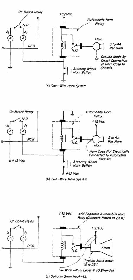
--- FIG.—19 Horn and siren wiring diagrams.
Construction Hints. Because of the complexity of the circuit, it is strongly recommended that all components be assembled onto a pc board. The pc board should be mounted onto a chassis and protected by a sturdy enclosure. This unit is best secured in a safe position in the trunk.
Jack J should be wired to the automobile chassis frame close to where the circuit enclosure is mounted. At least AWG No. 18 wire should be used and the connection tested to ensure that a good electrical contact has been made.
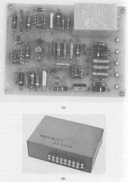
--- FIG.—20 Completed alarm project: (a) alarm electronics mounted on
a double-sided pcb; (b) chassis for alarm.
It is generally unnecessary to buy switches for the door, trunk, or hood, since these are often standard equipment on many cars. All existing switches should be checked for perfect working order. If a switch must be installed at any of the locations, the plunger type is most suitable for this application. A newly installed switch must be wired in parallel with either those using exit and entrance delay (door switches) or instant-on (trunk or hood). For example, hood and trunk switches should be wired in parallel with each other but not in parallel with the door switches (FIG. 18). Since diode D isolates the alarm circuit from the 12-volt source and all door switches are in parallel, only a single wire connection is necessary between J and the terminal connection on one door switch. In like manner, only one wire is necessary between J and either the trunk or hood switch.
Caution. Never attempt to switch any automobile horn directly with the pc on-board relay. These horns draw in excess of 3 amperes each and should be controlled only from the car’s horn relay. Depending on the type of automobile horn system, wiring according to FIG. 19a or b is recommended. As seen in FIG. 18, J and J have been left uncommitted for controlled switching of any particular type of horn circuit. This allows for convenient wiring connections to be made between J and J and any of the circuits shown in FIG. 19a, b, or c. If the car has no horn relay or if a siren is desired, an automobile horn relay must be installed. Sirens for alarm systems for use on a 12-volt dc source can draw in excess of 20 amperes. A horn relay capable of handling at least this much current must be selected. The siren, +12 volts, and ground connections should be made with a minimum of AWG No. 10 wire.
The finished security alarm package is shown in FIG. 20.