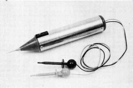
Companion instrument to the logic probe.
ALTHOUGH the logic probe used alone is a very valuable piece of digital test equipment, it is limited by the fact that it can only observe the logic states that occur naturally within the piece of digital equipment under test.
The logic pulser is a further valuable tool that is used in conjunction with the logic probe. It's function is to override the naturally occurring state at the particular circuit node under test. That is, if the circuit node is normally at the '1' state, the pulser will drive that node to a '0' for a very short period when the microswitch is pressed. If the circuit node is normally at a '0', the probe will drive it to a '1' for a very short period when the microswitch is released. Thus it puts a short pulse into the circuit node regardless of it's normal state when SW1 is pressed and released.
A fairly powerful pulse is required to override the normal logic state of a circuit node and care must be taken to ensure that the devices either driving, or being driven from that node are not damaged. This is achieved by making the pulse of very short duration. In our probe the pulse width is 500 nanoseconds. Thus although the pulse is of high current the energy released is insufficient to damage normal logic devices.
The probe must be suitable for driving either TTL or CMOS that is, it must operate from a supply ranging from 5 to 15 volts, it must be capable of operating into loads having a capacitance as high as 1000 picofarads and must supply a current pulse of around half an amp. All these conditions are fulfilled in the ETI 121 Pulser and the prototype has been tested by causing it to generate several hundred thousand half amp pulses without any problems. The probe is quite capable of pulling two ( in parallel) high- power TTL 'zeros' to a '1' level and this is the most severe condition it has to meet.
At the same time as providing high level pulses, the pulser should not draw too much supply current as some CMOS supplies may not have much additional capability. Under worst-case conditions the ETI Pulser drew a maximum of 10 mA.
-------------- A basic tool for digital servicing.
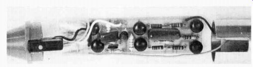
------------- Internal construction of the pulser.
The probe is capable of overriding a normal logic state but is not capable of overriding a point that is connected to ground or to a supply rail. Thus by pulsing a node and at the same time looking at that point with the logic probe it is possible to tell if that point is shorted to either rail.
The logic pulser combined with the logic probe is thus capable of performing stimulus - and - response testing of both TTL and CMOS logic and of determining the exact nature of a fault at a particular circuit node.
CONSTRUCTION
Construction is greatly simplified if the printed circuit board of Fig. 2, is used. This should have the components assembled to it in accordance with the component overlay. Note particularly the polarity of C1, and the connections of the microswitch such that the normally-closed terminal of the switch is connected to the base of transistor Q1. Also make sure that a red lead is connected to the positive rail of the board, and a black lead to the negative rail, to facilitate later connection.
We used the same probe case for the pulser as for the logic probe. The probe tip is again replaced by a darning needle and the microswitch SW1 is mounted into the plastic-section of the tip as follows.
First check the switch to determine what the contact arrangement is.
Attach COLOR coded wires to the switch, to aid later identification, and tape the microswitch into position.
Epoxy cement may then be used to fix the switch into place permanently.
Now cut a slot into the probe case so that the switch and plastic tip assembly can be inserted into the casing.
Connect the probe tip and microswitch leads to the board and, after insulating the inside of the case with cardboard or plastic as previously described, insert the board into the case. Pass the supply leads through the plastic end piece and then fit both end pieces and secure them in position.
Lastly attach Ezy-hooks or alligator clips to the supply leads.
Keep the supply leads as short as is reasonably possible as excessively long leads will degrade the performance of the pulser.
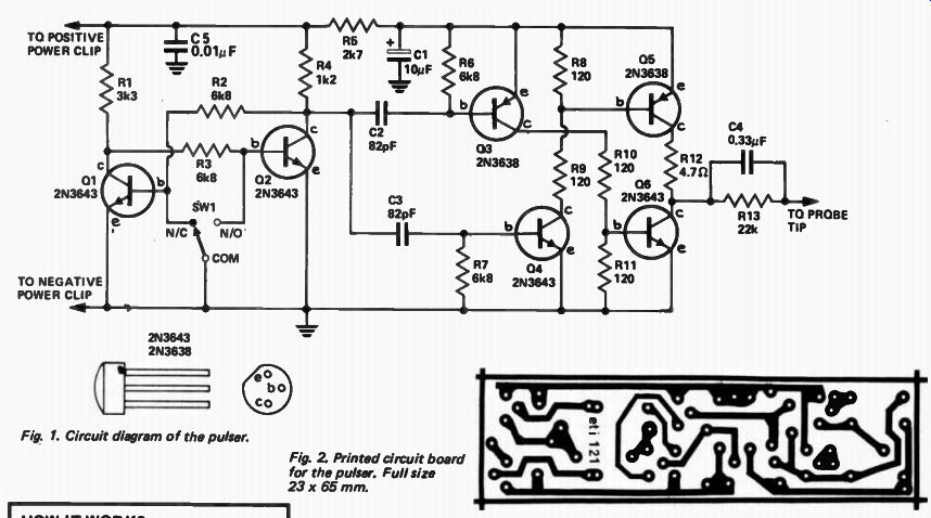
Fig. 1. Circuit diagram of the pulser.
Fig. 2. Printed circuit board for the pulser. Full size 23 x 65 mm.
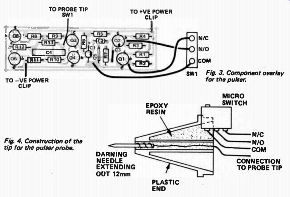
Fig. 3. Component overlay for the pulser.
Fig. 4. Construction of the tip for the pulser probe.
SPECIFICATION
-----------
PARTS LIST
R12
Resistor 4.7 ohm '4W 5% R,8,9,10,11 .. 120 ohm 1/4W 5%
R4 II 1k2 '4W 5%
R5 „ 2k7 '4W 5%
R1 .• 3k3 '4W 5%
R2,3,6,7 II 6k8 '4W 5%
R13 ., 22 k '4W 5%
Capacitor
C2,3
82 pF ceramic
C5 0.01 µF polyester
C4 II 0.33 µF polyester
C1 II 10 µF 25 V tantalum
Transistor
Q1,2,4,6
2N3643 or similar
03.5 .. 2N3638, 2N3638A or similar 1 micro-switch miniature McMurdo type 2LM 2 alligator clips or Ezy-hooks PC board ETI 121 probe case (see text).
---------------
HOW IT WORKS
The pulser is activated whenever microswitch SW1 is pressed. This switch controls the state of a flip-flop formed by transistors QI and Q2.
The flip-flop is necessary to prevent contact bounce of the microswitch from having effect.
The output transistors of the probe, Q5 and Q6, which in turn are controlled by Q3 and Q4 are both normally off. However when the microswitch is pressed 02 turns off and the rising voltage on its collector is coupled, via C3, to the base of Q4 turning it on. This in turn, turns on Q5 pulling the output to the positive rail. This generates a ' 1' pulse if the point under test was at a '0' level.
Resistor RI2 provides a current limit of around 500 milliamps. Due to the small value of C3 the pulse output is only about 500 nanoseconds long, short enough so that there is insufficient energy to damage the device under test.
When the switch is released Q2 turns on and the negative-going edge is coupled to Q3 by C2 turning it on.
This turns on Q6 causing the output to be pulled to the negative rail. This gives a '0' pulse which, like the ' 1' pulse, is only 500 nanoseconds long.
The output from the probe is taken via the paralleled combination of R13 and C4 where C4 carries the current and R13 discharges C4 between pulses. This network protects the probe against the condition where the probe is inadvertently connected to a voltage which is above or below the logic supply rails.
Resistor R5 isolates the high current pulse from the power supply, capacitor C1 providing the actual current needed.
--------