A basic tool for digital servicing.

THE SERVICING of digital equipment is greatly simplified by the use of a logic pulser and logic probe, for these two instruments enable one to follow circuit operation stage by stage.
THE PROBE The probe must be capable of detecting pulses as short as 50 nanoseconds (for TTL operation) and make them visible. It was found that readily available linear ICs were not suitable as they are too slow and required dual supply voltages. Neither could CMOS be used as it also is too slow, for testing TTL gates, and its threshold voltages are not consistent.
Further, TTL could not be used as it cannot withstand the voltages used with CMOS logic. This virtually means that the only devices that are suitable are discrete transistors.
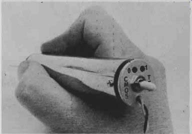
----------- The logic probe seen from the rear.
HOW IT WORKS
The probe consists of two independent voltage level detectors which, via pulse stretching monostables, drive light-emitting diodes to give a visual indication of the logic state being monitored.
Transistors Q1 and Q4 form the low level or '0' detector, transistors Q5 and Q6 the high level or ' I' detector whilst the remaining components form the pulse stretching monostables and visual indicators.
The high level detector works as follows. If the input level is below about 2.5 volts ( 1.3 volts above the level set on R17 by transistor Q5) transistor Q6 will be cut-off. When the input level rises above 2.5 volts, transistor Q6 will turn on, as will Q7, causing LED 2 to light - indicating a '1'. The transition at the collector of Q7 will, at the same time, be passed to Q8 turning it off. The current which was flowing through Q8 will now flow via R22 in to the base of Q7 holding it on even though Q6 may by now have stopped conducting. After fifty milliseconds the charge on C2 will leak away via R19, 20 allowing Q8 to conduct.
When Q8 conducts it robs the current from the base of Q7 turning it and the LED off. However should the voltage at the tip of the probe still be present Q6 will still be turned on holding on in turn q7 and the LED. Resistors R11, 12, 13 and 14 set the operating conditions of Q5 such that the threshold voltage is optimized for either TTL or CMOS. As CMOS logic works on supply voltages ranging from five to fifteen volts, transistor Q5 has been arranged to track the supply so that the correct threshold is maintained at all times.
The low level detector works in exactly the same fashion except that it is inverted in order to detect pulses which approach within 0.45 volts of the negative line (TTL only). Each PNP transistor and each NPN transistor have been replaced with their complements. In this case Q4 sets the thresholds and the circuit operates exactly as stated for the high detector. Note that the diodes have also been reversed.
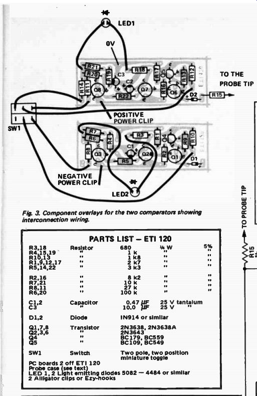
Fig. 3. Component overlays for the two comparators showing in wiring.
-------------
PARTS LIST - ETI 120
R3,18
Resistor .680 R4,15,19 1 k R10,13 1 k8 R1,9,12,17 " 2 k7 R5,14,22 3 k3 R2,16 R7,21 R8,11 R6,20 C1,2 C3 e
• Capacitor 8 k2 10 k 27 k 100 k
0.47 uF
25 V tantalum 10.0 uF 25 V
D1,2 Diode IN914 or similar Q1,7,8
Transistor 2N3638, 2N3638A Q2,3,6 2N3643 Q4 BC 179, BC559 Q5 " BC109, BC549 SW1 Switch Two pole, two position miniature toggle PC boards 2 off ETI 120 Probe case ( see text)
LED 1, 2 Light emitting diodes 5082 - 4484 or similar 2 Alligator clips or Ezy-hooks 5 %
-------------------------
CHARACTERISTICS
PULSER - ETI 121
• Will source, or sink, up to 500 mA.
• Operates on supply voltages from 5 to 15.
• Suitable for both TTL and CMOS. e Power supply drain less than 15 mA under worst case conditions.
• Press for ' 1' release for '0'.
High impedance at other times (> 1 M). e Will drive capacitive loads up to 1000 pF.
• Protected against accidental reversal of supply leads.
• Duration of pulse 500 nanoseconds.
PROBE - ETI 120
• Pulses as narrow as 50 nanoseconds will be detected.
• Stretches narrow pulses to 50 milli-seconds for ease of detection.
• Operates on supply of 5 to 15 volts.
• Suitable for TTL or CMOS.
• True ' 1' and '0' level detectors. Neither LED is alight if the circuit is faulty or the probe is not making contact.
• Current drawn from the circuit is less than 20 microamps.
• Current drawn from power supply ( on a LED alight) 12 mA on 5 volts, 35 mA on 15 volts.
-------------------------
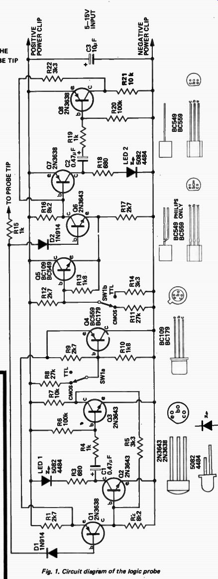
Fig. 1. Circuit diagram of the logic probe
Fig. 2. Printed circuit board for the logic probe (2 required). Full size
23 x 66 mm.
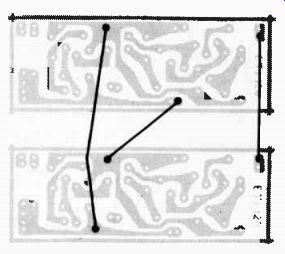
Fig. 4. Linking required between the two boards.
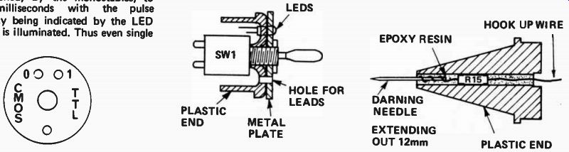
Fig. 5. Artwork for the nameplate on the probe.
Fig. 6. How the probe ends are constructed.
------------------------
As both high and low logic states must be detected, a discrete transistor voltage- comparator circuit was designed to detect each state separately. These comparators must not load the circuit under test as CMOS is sensitive 'to current and capacitive loading. In our prototype the current drawn was a maximum of 19.7 microamps for a high, and 10 microamps for a low.
In both comparators the transistors associated with the pulse detector are turned on by an input level that exceeds the comparator threshold.
As transistor turn- on time is much faster than turn-off time, using the transistors in this way ensures the highest possible speed of operation for the particular types of transistors used.
Additionally, the delay in turning off assists by lengthening the pulse, thus ensuring more reliable triggering of the monostable on very short pulses.
The input transistors Q1 and 06 are protected against breakdown, due to excessive base-emitter voltage, by diodes D1 and D2. The diodes are also required to ensure that Q1 and 06 remain conducting even when the probe tip is taken to the supply voltage.
Transistors Q3 and Q8 are also protected against reverse base- emitter voltages by R4 and R19 respectively.
In operation the probe will light LED 1 if a low level is detected, LED 2 for a high, neither LED if the point being monitored is at ground potential or a poor contact is made with the tip, and both LEDs will light if there is a pulse train present.
A single pulse input will be lengthened, by the monostables, to 50 milliseconds with the pulse polarity being indicated by the LED which is illuminated. Thus even single pulses as short as 50 nanoseconds may readily be detected.
CONSTRUCTION
We built our probe onto two small printed circuit boards and assembled it into a small, commercially-available probe case. The two printed-circuit boards are identical and care should be taken to use the correct overlay for each board as different transistors are used and some components are reversed on the two boards. Note particularly diodes D1 and D2 and capacitors C1 and C2. Also note how the two boards are linked together and that the supply rails are reversed. No difficulty should be experienced if the printed- circuit boards and the component overlay as specified are used.
The probe case used in our prototype was one manufactured by Jabel. The case has a length of 102 mm and an internal diameter of 23 mm. The probe tip, as fitted, is rather large and awkward. We therefore replaced the tip, with a darning needle, as shown in Fig. 6. The fine point of this tip is much easier to use on micro circuitry and, as it is very sharp, it will penetrate varnish etc to make reliable contact. A needle is a little brittle and for this reason it is recommended that a maximum unsupported length of 12 mm be left protruding. Resistor R15 is mounted within the tip and soldered directly to the needle. The other end of the probe is fitted with a plastic stopper which is used to support SW1 and both LEDs. SW1 is also used to hold a small name-plate in position as shown in Fig. 6. Two LEDs are mounted into the end plate, together with SW1, and after soldering leads to the LEDs they should be passed through the holes in the plate, and the plastic end- piece, and secured in position with a drop of epoxy cement. Another hole is drilled in the stopper through which is passed the two supply-voltage leads.
Connect the leads from the stopper assembly to the previously assembled boards. Position the boards together, copper side to copper side, with a piece of insulating material between them. Make sure that the board assembly will fit in to the tube without fouling the sides. Cut a piece of cardboard or plastic 75 x 85 mm, roll it into a tube and fit in the probe body. Now fit the board assembly into the tube - it may be necessary to dress the sides of the boards with a file to obtain a neat fit.
The tip may now be connected and both ends screwed into position.
Finally, alligator or, better still, Ezy-hooks clips should be fitted to the supply leads.
---------