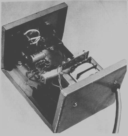
Simple, adjustable power source has innumerable applications.
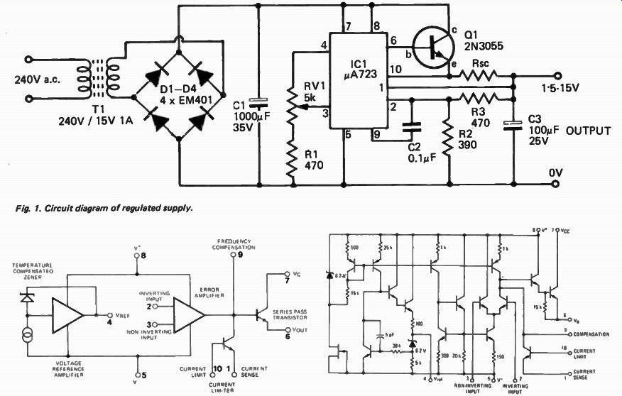
Fig. 1. Circuit diagram of regulated supply.
Fig. 2. Simplified schematic of uA723. Circuit schematic of IC uA723.
IN June 1971 we published constructional details of a ' Logic IC Power Supply' which was specifically intended to power RTL and TTL circuitry. Since then we have received a surprisingly large number of requests to provide details of a similar unit with an extended voltage range.
Here then are details of a simple yet versatile power supply capable of delivering 1 amp up to 10 volts and 1 / 2 amp up to 15 volts.
The unit may readily be adapted to operate over other voltage and current ranges.
As with the previous unit, refinements such as output voltage and current metering, variable current limiting etc. may be added to the basic circuit.
VOLTAGE REGULATOR IC
The control circuit of this supply is formed by the integrated circuit precision voltage regulator - shown as IC1 in Fig. 1. This IC is now produced by a number of companies including SGS, Fairchild and Motorola (respective type numbers are included in the parts list for this project). The integrated circuit is a monolithic voltage regulator constructed on a single silicon chip using the planar epitaxial process. The device consists of a temperature compensated
-----------
-ETI111
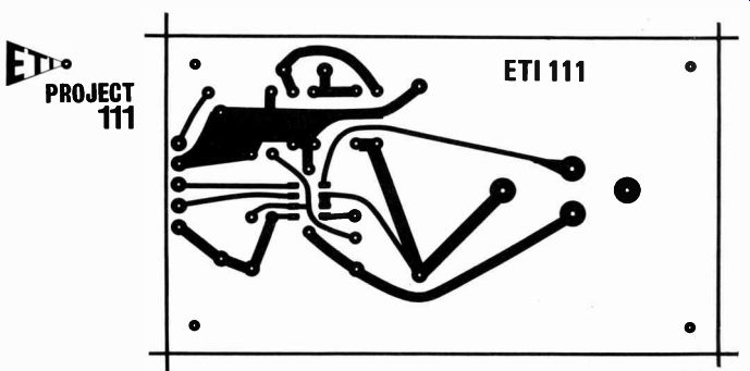
Foil pattern for logic power supply (actual size reference amplifier, error amplifier, power series- pass transistor and current limiting circuit. Additional external npn and pnp pass elements may be used when output currents exceeding 150mA (from the IC) are required. Provision is made for adjustable current limiting and remote shut-down. In addition to this the IC features low standby current drain, low temperature drift and high ripple rejection.
------------
HOW IT WORKS
Figure 2 shows a simplified equivalent circuit of ICI. The voltage reference amplifier produces (typically) 7.I5V at pin 4, this voltage has a maximum temperature coefficient of 0.015%/°C. The Vref voltage is taken to potentiometer RV I which enables it to be varied between 0.7V and 7.15V. The error amplifier ( within the IC) drives a power transistor ( also within the chip), and this in turn drives the external series pass transistor Ql.
The output of Q1 is divided by R2 and R3 (+2.2) and this voltage provides the feedback signal for the error amplifier. Hence the output voltage will be approximately 2.2 times the voltage on RV 1. Current limiting is determined by the voltage drop across RSC. If this exceeds 0.6V, the current limit transistor within the IC becomes forward biased and bypasses any further increase in drive current from the output stage.
The max. output voltage and current of this unit is a function of the transformer, filter capacitor, and the heatsinking of Ql. The prototype unit used a 15V centre tapped IA transformer (AR 2155) and this provided IA up to 10V and 1 / 2A at 15V. The drop in output current is due to rectified de voltage decreasing on load. If a higher voltage transformer is used - or one with a higher current rating, thus providing better regulation - then higher output currents may be expected.
The maximum output voltage may be altered by changing the ratio of R2 and R3. Note that the maximum no-load voltage across Cl should not exceed 35V.
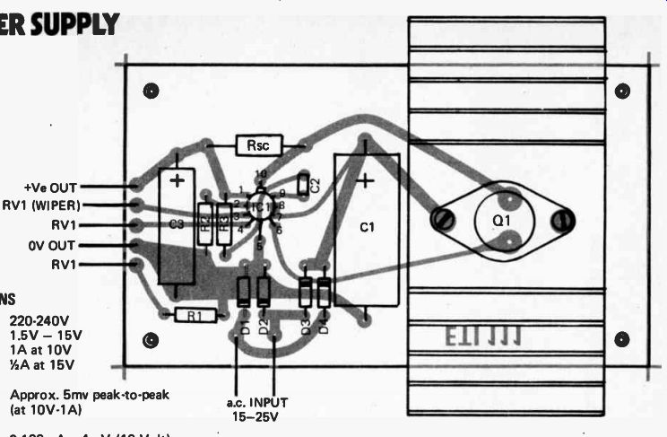
Fig. 3. Layout of components on circuit board.
-------
SPECIFICATIONS
Input Voltage Output Voltage Output current 220-240V 1.5V - 15V 1A at 10V 'AA at 15V
Ripple Regulation Approx. 5mv peak-to- peak (at 10V- 1A)
0-100mA = 4mV ( 10 Volt)
0-1.0A = 20mV ( 10 Volt)
---------------
RSC - TYPICAL VALUES Value of RSC Current Limiting 10 ohms 65mA 1 ohm 650mA
0.5 ohms 1.4A
0.2 ohms 3.2A
--------
CONSTRUCTION
Our prototype unit was built on an epoxy glass board, however the constructional method is not critical and the unit may alternatively be built on matrix board, tag strips etc.
The power transistor is mounted on a 2" strip of extruded heatsink which in turn is located on the printed circuit board by the same screws that locate the transistor. One of these screws is also used for the electrical connection for the collector of the transistor.
The IC may be soldered directly into the circuit - ensure that the device is correctly orientated - and avoid excess heat. Recommended maximum lead temperature during soldering is 300°C. A load sensing resistor ( RSC) is used to provide overload protection. In our prototype we used a short length of resistance wire cut to length to limit the current to the desired value. An interesting alternative is to substitute a 20 ohms 5 Watt wire-wound potentiometer for RSC. This enables the current limiting facility to be step-lessly varied. With this feature the user can start experimenting with a very low current limit and then increase the current when the circuit is operating correctly.
The basic circuit described in this article can be modified to provide other ranges of voltage and current.
The main design limitations are that the voltage across the IC must not exceed 40V and that the output current from the IC must not exceed 150mA, or 800mW of power.
Transistor Q1 (2N 3055) is capable of dissipating up to 115 watts but if power levels of this magnitude are envisaged then a second transistor should be added, in a Darlington pair configuration, to transistor Q1. This will reduce the loading on IC1. A larger heat sink will also be required.
INCREASED RIPPLE REJECTION
The integrated circuit chosen for this project has a typical ripple rejection of 74 dB. This is more than adequate for most applications. However by additional filtering at the non-inverting input ( pin 3), the ripple can be even further reduced. A typical performance, using a 4.7µF capacitor across the non-inverting input and Vrer is approximately 86 dB.
-----------
PARTS LIST------ ETI 111
R1 R2 R3 RSC RV1 Dl- D4
01 IC1 C1 C2 C3
T1 resistor 470 ohm 1 / 2W 5% resistor 390 ohm 1 / 2 W 5% resistor 470 ohm 1 / 2 W 5% see text potentiometer 5k linear diodes EM401, 1N4005 or similar transistor 2N3055 integrated circuit uA723 (or SGS L123, or MC1723CG) (metal can types) capacitor 1000 uF 35V electrolytic capacitor 0.1 uF 100V capacitor 100 uF 25V electrolytic transformer 240V primary 15-20V sec @ lA PC board ETI 111 on-off switch, terminals, knob, 3 core flex and plug, metal box approximately 4 1 / 2 x 3 1 / 2 x 6 etc.
-------
--------