By BARRY WILKINSON
Specifically intended for powering experimental integrated circuit projects, this power unit features independent positive and negative supplies - but with automatic tracking when required.
UNTIL recently, integrated circuits were priced beyond the reach of the average enthusiast, and very few constructional projects specified their use.
But as with so many electronic components, mass production and wide-spread commercial acceptance has resulted in quite dramatic price reductions, and integrated circuits costing twenty or thirty dollars a couple of years ago, are now readily available for well under two dollars. Many cost less than a dollar.
From the enthusiast's point of view this is a most exciting development for it opens up the possibility of constructing far more ambitious projects than were previously feasible using discrete components. Many such projects are featured in Electronics Today International.
But there is one minor drawback to integrated circuits and this is that many of them require both positive and negative power supplies. These supplies must also have a better level of line and load regulation than was previously necessary.
The power supply described in this project has beer designed specifically for this purpose. It is intended for both the serious enthusiast and the professional development engineer.
As may be seen from the specifications, its performance is equivalent to many commercially built units at many times the price.
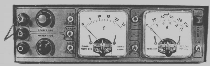
The unit has two outputs, one positive, and one negative - each separately ad!ustable from zero to 20 Volts, or settable in such a way that the negative supply automatically tracks the positive supply.
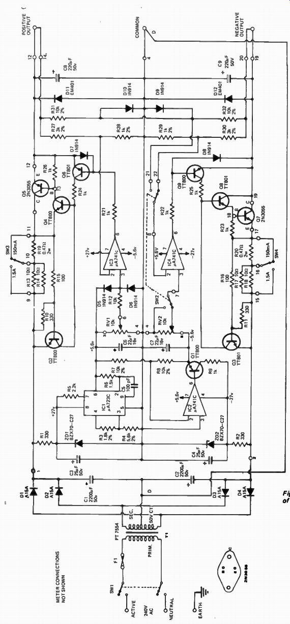
Fig. 1. Circuit diagram of complete unit.
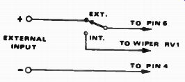
Fig. 2. Circuit modifications for externally programming positive rail
(see text).
CURRENT LIMITING
Both the unit, and your experimental circuits, are protected against damage by current limiting network s incorporated within the power supply.
A panel mounted switch is used to select the maximum desired current at either 190 mA or 1.80 Amps. If this level is reached, the output voltage will drop and current will be held at the selected limit.
For the professional user of this unit, provision has been made for the positive regulator to be externally programmed. The necessary wiring changes are shown in Fig. 2.
Due largely to the use of externally mounted heatsinks, and the use of integrated circuits in the control and voltage reference circuits, the complete power supply unit is quite small and compact. Yet despite this, the internal layout is spacious and all major components are readily accessible.
CONSTRUCTION
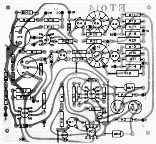
Fig. 4. How the components are Mounted on the printed circuit board.
Compare this with Fig. 3.
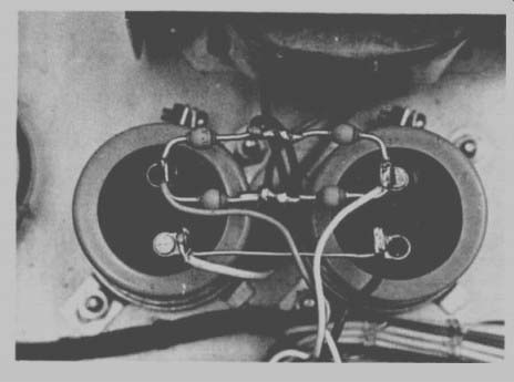
Fig. 5. Diodes D1 - D4 are mounted on top of the filter capacitors.
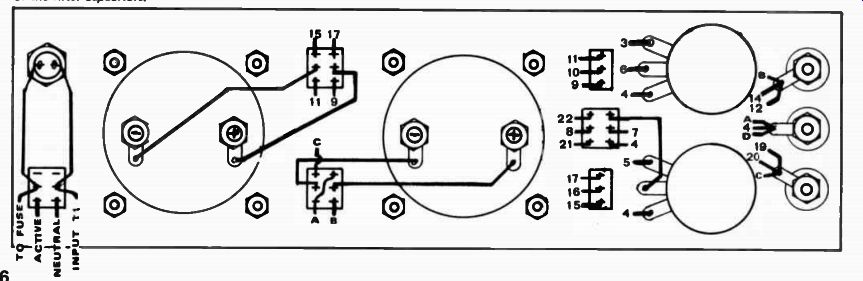
Fig. 6. This drawing shows front panel wiring details. Wires A, B and Care
interconnecting wires on the front panel. Wire D goes to the common of the
filter capacitors.
Construction is reasonably straightforward if work progresses in the correct manner. The unit may be assembled on matrix board, but we strongly recommend that the correct printed circuit board be used. The foil pattern of the p.c. board is shown in Fig. 3.
Assuming that the printed circuit board is used, commence construction by inserting the pc board pins into the positions numbered on the board.
These pins should be inserted with the flange (if flanged) on the component side of the board. All external wiring to and from the printed circuit board will be attached to these pins on the foil pattern side of the board.
When installing the integrated circuits ensure that they are orientated correctly before soldering. ( Note that Fig. 4 shows all components, including integrated circuits, as seen from the component side of the board.) Small heatsinks are fitted over transistors 04 and 08. Ensure that these do not contact any other component by mounting them about 1/8" above other nearby components.
When all components have been mounted on the board, recheck for correct orientation and polarity.
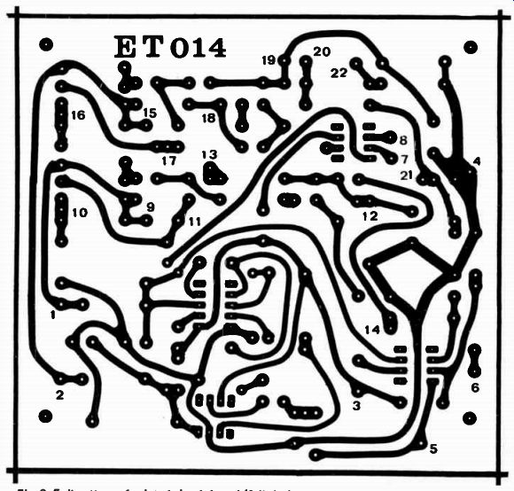
Fig. 3. Foil pattern of printed circuit board (full size).
Now mount the transformer and the filter capacitors onto the chassis.
Locate diodes DI - 04 on top of the filter capacitors as shown in Fig. 5.
The heatsinks must now be drilled to take the two 2N3055 output transistors. Carefully remove any burrs from around the holes and then mount the transistors preferably using McMurdo type 2210-01- anodized insulating washers. If available, use a smear of silicon grease between transistors and the heatsinks - this will further improve heat transference.
Finally, check insulation between the transistor and the heat sink, and then fit the McMurdo type 9151-09-01 transistor covers.
On our prototype unit we constructed our front panel by sandwiching a line drawing between the chassis and a piece of smoked perspex. This provides a very professional looking appearance. An even better finish can be obtained by using an anodized aluminum panel, and these may be available from parts suppliers, obtained by using an anodized aluminum panel, and these may be available from parts suppliers.
Having determined the method of finishing the front panel, assemble all the relevant components onto the panel.
Wires should now be attached to the pins on the underside of the printed circuit board. Insulated 14/0076 wire should be used for this purpose. Two wires should be attached to pins 9, 12, 17 and 19, three wires attached to pins 11 and 17, and four wires attached to pin 4. All wires should be either COLOR coded or marked so that they may be clearly identified.
-----------
Output Voltage Output Current
Current Limiting Meter Ranges (current)
(voltage)
Line Regulation Load Regulation Ripple Output Impedance
SPECIFICATION - POWER SUPPLY
0 - 20 Volts positive
0-20 Volts negative
0 - 1.5 Amps 190 mA and 1.80 Amps 150 mA and 1.5 Amps 25 Volts better than 1 mV for 15 Volt input voltage change less than 10 mV drop from no-load to full load less than 2 mV peak to peak 7 mn@ dc - 1.5 kHz 14 mn@ - 3 kHz 56 mn@ - 15 kHz 200 mn@ - 100 kHz
----- COVER 60100
DUAL POWER SUPPLY
113g steel
BASE ET105
DUAL POWER SUPPLY 168 steel plated/ NOTE: The power supply is short circuit proof but shorts in excess of 30 seconds should be avoided due to excessive power dissipation in the transistors.
---------
The printed circuit board should now be mounted onto the chassis and the wires loomed to their respective destinations. Note that one each of wires 11, 12, 17 and 19, together with wires 13 and 18 go to the back of the unit and to the heat sinks. Wires 1 and
--------------
R1 R2 R3 R4 R5 R6 R7 R8 R9 R10 R11 R12 R13 R14 R15 R16 R17 R18 R19 R20 R21 R22 R23 R24 R25 R26 R27 R28 R29 R30 R31 R32 CI C2 C3 C4 C5 C6 C7 C8 C9
01 - D4
05 - D10 Dll - 012 ZD1 ZD2 QI Q2 Q3 Q4 Q5 Q6 Q7 Q8 Q9 ICI IC2 IC3 IC4 SW1 SW2 SW3 SW4 SW5 SW6 TI RV1 PARTS LIST ET105
- resistor 330 ohm
- " 1.8k, 2%
- " 5.6k, 2%
- " 2.2k
- " 1.5k
- " 10k, 2% 10k, 2% " 1k
- " 330 ohms
- " 330 ohms
- " 10k
- " 10 ohms
- " 10 ohms
- " 100 ohms
- " 100 "
- " 10 "
- " 10 "
- " 0.47 ohms, 2 Watt, ASW2 II 0.47
- " 1k
- " 1k
- " 1k " 1k
- " 1k
- " 1k
- " 3k, 2%
- " lk, 2%
- " lk, 2%
- " 3k, 2%
- " 10k, 2% " 10k, 2% (all resistors are 42 Watt 5% unless otherwise stated, The 2% resistors are Pye type TR5 or equivalent)
- capacitor, 2200uF, 50 Volt, Elna type PG 25uF, 50 Volt, Elna type RB e. re el I. F. OR 100 pF. 22uF, FP 2201./F, 50 Volt, Elna type RB ft le PI OP el P. I. diodes type Al5A or equivalent.
" 1N914 " " EM401 " zener diode type BZX70 C27 transistor type TT800 el TT801 TT800 " 2N3055 " TT801 " 2N3055 " TT801 " TT800
- - integrated circuit type 1.IA 723C " 1./A 741C " µA 741C IF " j .LA741C (all the above ICs are metal can type).
- miniature switch, double-pole changeover, 240 Volt, Plessey C & K type 7201 or similar.
RV2 Sundries TOS Heatsinks, - 2 off, McMurdo TXBF 032 025 CB Power transistor heatsinks, 2 off, Mullard 35 DB 3C drilled to suit. Two transistor covers, McMurdo 9151 09 01. Two anodized insulating washers, McMurdo type 2210 01 01. One set of metalwork. One front panel. 240 Volt neon panel light. Three terminals. Two potentiometer knobs. One fuse holder for size 00 fuse. One 1 Amp size 00 fuse. One 3 core flex and plug. One cable clamp. One printed circuit board ET 014. Twenty two pc pins McMurdo type 5737 54 08. Three grommets. Four rubber feet. Four 3/4" spacers.
14/0076 connecting wire ( insulated) various screws, washers, nuts etc.
Voltmeter - 25 Volts fsd, 242" square, Ferrier type B 23 or equivalent.
Ammeter - 750 mV fsd, 1 mA, scaled 1.5 Amps and 150 mA. Ferrier type B34 or equivalent. ( when ordering, specify that meters should be scaled for steel panels). 16 Volt, tag tantalum type " single pole changeover, C & K 7101 " double pole changeover, C & K 7201 t.
transformer, A & R type PT 7554, 50 Volt, centre tapped, 1.5 Amp.
- potentiometer, linear, 10k, Plessey type E or equivalent. .9 F.
-----------------------
2 go to the filter capacitors and a wire D comes from the common of the filter capacitors up to the loom and to the common terminal on the front panel.
The front panel can now be wired as shown in Fig. 6.
The wires to the heat sink mounted transistors are taken through the grommets provided, and the already assembled heat sinks mounted into position.
Complete all remaining wiring taking care that all leads carrying 240 Volts are adequately insulated. The mains lead must enter the case through an insulating grommets and the lead must be securely anchored to the case. It is HOW IT WORKS.
The mains input voltage is reduced and isolated by transformer T1. The 25-0-25 Volt output from the transformer is then rectified and filtered by diodes D1-D4, and capacitors C1 and C2 to provide an unregulated ± 40 Volt dc supply.
Series regulators are used in the main control system. The two regulators - one for each supply - are almost identical in operation, therefore only the positive regulator will be described in detail.
The series pass transistor Q5, is mounted on an external heat sink.
Transistors Q4 and Q6 provide current amplification for Q5 giving the combination a total current gain exceeding 50,000. The voltage gain is approximately unity.
The main reference supply is generated by IC1 which is a precision voltage regulator. The reference level required is obtained by potentiometer RV1 which is connected across the 5.6 Volt regulated output from IC1.
Power for the IC voltage reference is supplied by R1, ZD1 and C3. This maintains a constant voltage across the IC, eliminating variations due to changes in mains voltage. The 27 Volt supply from this circuit is also used to supply power to IC3.
The reference for the negative supply is obtained from operational amplifier IC2 which is connected so as to track the positive reference supply. The 5.6 volt output from this circuit is just as accurate as the output from the main regulator.
Power for this operational amplifier is supplied from a 27 volt zener which is also used to supply IC4.
The power supplies for ICI are + 27 Volt and 0 Volts; for IC2 and IC4, the supplies are + 5.6 Volts and 7 27 Volts; for IC3, + 27 Volts and - 5.6 Volts.
Resistors R27 and R28 divide the output voltage by four. This voltage not sufficient merely to tie a knot in the mains cord - this is a dangerous practice.
The supply should now be ready for use, but before connecting to the mains, recheck all poi nt - to-point wiring and all soldered connections.
One point that may not be commonly realised is that meters are calibrated specifically for one panel material. A meter calibrated for mounting on a steel panel may be as much as 30% out if it is mounted on an aluminum panel - and vice-versa.
We recommend that a steel chassis is used for this project - but if you decide to use aluminum notify the meter supplier accordingly.
-------------
is compared against the voltage set by RV1 by operational amplifier IC3.
The output of IC3 controls the series regulator configuration, and hence the output voltage. The action of IC3 is to keep the two voltages at its input at the same level. Thus, the output voltage will be four times the input voltage, and virtually independent of load current.
When load current approaches the level set by the limit switch, transistor Q2 becomes forward biased sufficiently to cause it to conduct.
This bypasses current from the base of Q4 and causes IC3 to lose control of the output. If the load continues to increase, the output 4oltage will fall and the current will remain effectively constant.
The negative regulated supply works in the same manner when the power supply is used in the normal mode.
A tracking mode of operation is also included, and in this mode the negative supply tracks the positive supply. If, for example, the positive regulator is set at + 14.5 Volts, then the negative supply will automatically be set at - 14.5 Volts.
In the tracking mode of operation, the reference voltage is zero volts and the voltage used as the output voltage reference is the centre voltage of the two supplies. And since the IC tries to maintain both inputs at the same level ( in this case zero volts) then the two output voltages must be of the same value.
Diodes D7 through D12 are used to protect the integrated circuits and output transistors against various forms of misuse, including shorting the positive and negative outputs together.
Provision has been made in the design for externally programming the positive regulator. If this facility is required, alter the wiring as shown in the Fig.
(Resistor R12, and diodes D5 and D6 protect the IC when this mode of operation is employed).
-------------
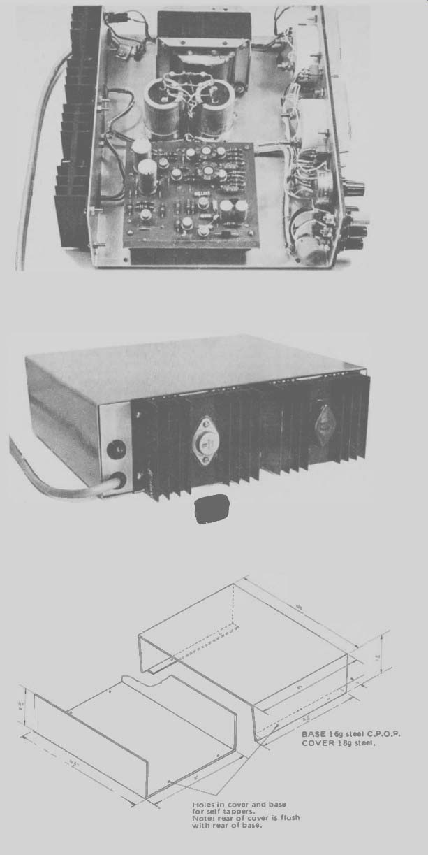
Holes in cover and base for self tappers.
Note: rear of cover is flush with rear of base.
BASE 169 steel C.P.O.P. COVER 18g steel.
-----
--------