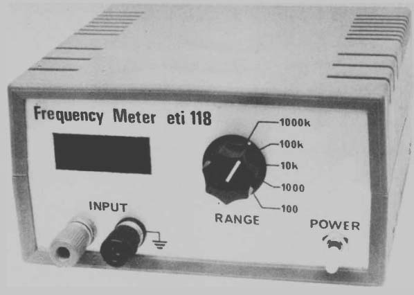
Inexpensive unit works to 1 MHz.
WE CONTINUE our series of simple units, based on the ETI 533 Display Module, by describing a simple frequency meter. The unit is easy to construct and quite inexpensive.
DESIGN FEATURES
We originally considered that this project would only take a short time to develop -- but were we ever wrong! Just about everything that could have gone wrong did so, and we became convinced that Murphy was not only alive and well but was living in Rushcutters Bay.
The first problem was to choose suit able timebase circuitry. As the project had to remain fairly economical to build, the use of a crystal timebase was ruled out. We eliminated a mains referenced timebase because it was considered that the possibility of battery powered operation was a definite advantage. Especially as control tones on the mains can cause problems.
An NE555 timer was tried for the 10 second timebase but it soon became apparent that the device just was not stable enough even when the power supply was regulated. The change in frequency due to supply changes was about 1.5%/volt. And even with a regulator the stability was not good enough to allow more than four digit readings. The error occurs because the N E555 output stage does not go exactly to the supply rails but only 0.6 V away from them. The same applies to the discharge transistor which has a fixed saturation voltage.
We considered many oscillator designs in an effort to find one with a stability of better than one part in 10,000 and ultimately chose the one shown in the circuit diagram. This type of oscillator is well known but is not normally considered to have good accuracy and stability. This is because in a conventional op-amp IC there is normally a base-emitter junction at the output, as in the 555. However in the new CA 3130 device this problem has been eliminated as the output stage is CMOS and appears as a resistance (about 500 ohms) and not as a voltage drop. A further advantage of this IC is the extremely high input impedance which eliminates any inaccuracies due to loading effects. On the prototype the frequency change was less than one part in 10 000 with a supply voltage change of from 8 to 16 volts.
The main source of error is now due to the temperature coefficient of R10.
The expected error, using good quality metal-film resistors would be around 0.01% per degree C. The CA3130 IC is also ideal for the input stage, because of its high input impedance, and also because it allows a 0 V reference to be used thus eliminating the centre-tap point normally required for conventional operational amplifier circuits.
-----------
SPECIFICATION
INPUT IMPEDANCE INPUT SENSITIVITY 10 Hz to 10 kHz RANGES DISPLAY ACCU RACY STABILITY OVERLOAD PROTECTION up to 100 kHz 100 kHz to 1 MHz POWER
470 k // 47 pF
< 50 mV rising to 1 V at 1 MHz 99.9 Hz to 999 kHz 3 digits ( no overload indication) as calibrated.
0.01% can be expected but depends on resistor stability.
50 Vac. dropping from 50 Vac to 10 Vac 50 Vdc. 240 Vac or 12 Vdc at 100 mA.
-------------------
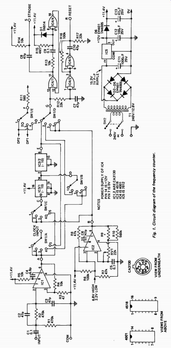
Fig. 1. Circuit diagram of the frequency counter.
-------------
PARTS LIST
R3 Resistor 47 ohm R11 560 R4,5,13,14 " 10 k R17 22 k R12 " 33 k R7,8 re 47 k R6,16 " 100 k R1,2 er 470 k R10 ., 560 k R15 4M7 R9 ( See table 1)
1 / 4 W I/AW "W 1 / 4 W VAN 1 / 4 W 1 4W 1 / 4 W 5% 5% 5% 5% 5% 5% 5% 5% 2% 5% C4 Capacitor 6.8 pF ceramic C2,3,6 " 47 pF ceramic C7,8,10 " 47 pf ceramic C1,5,9 " 0.1 ¡IF 100v poly ester C13 47 I.LF 25 V electro C12 1001./F 25 V electro C11 1000uF 25 V electro DI Diode IN914 or similar D2'-06" EM401, IN4005 or similar IC1,2
Integrated Circuit
CA3130 (AWV) IC3 " •4518 (CMOS) IC4 " 4001 ( CMOS) IC5 " 7812 ( plastic pack). SW1 Rotary switch 6 pole 5 position SW2 toggle switch DPOT ( miniature)
T1 transformer 240 V/12.6 V 150 mA PC Board ETI 118 Case type PCI (A&R Soanar) or similar Display Module - ETI 533 Shield as per Fig. 7.
Front panel as per Fig. 5.
3 plain spacers 6.4 mm long insulated 3 plain spacers 19 mm long 3 1/8 whit. spacers 25 mm long One 8 way tag strip 3 core flex plug, grommet and clamp pc board pins 3 25 mm long 1/8 whit. screws 9 12 mm long 1/8 whit. screws 6 1/8 nuts.
Two input terminals ( red- black)
-----------------------
PARTS AVAILABILITY
The CMOS ICs used in this project are distributed by CEMA and TOTAL.
---------------------
HOW IT WORKS - ETI 118
The frequency counter may be divided into several basic sections.
a. Input amplifier - Schmitt trigger.
b. 10 Hz oscillator.
c. Two divide by 10 networks.
d. Strobe and reset circuitry.
e. Power supply.
f. Display module ( ETI 533). The input amplifier is a CA3130 connected as a Schmitt trigger.
Resistors R3 and R4 provide positive feedback whilst resistor R2 provides protection for the input of the IC. The resistor R5 is used to increase the negative slew rate of the amplifier thus increasing the range of operation to one megahertz.
The 10 Hz oscillator is another CA3130 where positive feedback is applied by R8 and negative feedback by RIO. When the output is high the voltage at pin 6 is about 6.8 volts.
The capacitor C5 charges via R10, and when it reaches 6.8 volts the output goes low. The voltage now set at pin three is 2.2 volts and the output remains low until C5 has discharged to this point at which the output goes high again. Preset RV1 varies the oscillator frequency by about 4% and a parallel resistor, R9, is required to set it within the required adjustment range. A higher value preset could be used but it becomes difficult to adjust with accuracy.
The divide by ten circuitry is simply a 14518 IC which contains two decade counters. It can be switched to divide the input frequency ( 100 k, 1 M ranges) or the timebase ( 100 Hz, 1 kHz ranges) by means of the range switch SW!. The timebase, be it ten seconds, one second or 0.1 seconds, is coupled by SW1/d to IC4/1 pin 13. When this voltage goes high the output of IC4/1 goes low and C1 couples a short negative going pulse into the strobe terminal of the display module. After a short time, due to R12 and C7, the output of IC4/3 goes high and C10 couples a short positive pulse into the reset terminal of the display module.
When the output of IC4/ 1 goes low the output of IC4/4 goes high and the output of IC4/1 remains low irrespective of what now occurs at pin 13. After about 350 milliseconds C9 recharges via R15 releasing IC4/1 to the control of the timebase. This procedure removes three out of every four strobe pulses when using the 10 Hz timebase, making the display easier to read.
The resistor R16 is used to raise the steady-state voltage at the reset terminal to about 1.8 volts, thus ensuring that the reset pulse goes high enough to give reliable triggering. The voltage at the strobe terminal sits at about 10.4 volts due to the 100 k input impedance of the display module.
The power supply is a full-wave rectifier and capacitor filter supply which is regulated down to 12 volts by a 7812 regulator IC. The control circuitry is isolated by a diode D6 and capacitor C13 to prevent any ripple appearing on the 12 volts due to the current drawn by the display module.
The display module contains a three decade counter-store-decoder and display as described on page 22.
To measure frequency all that is needed is to count the number of pulses occurring over a given period of time. If we count the number of input pulses over a one second period we can measure to the nearest one cycle, or one hertz. If a three digit display is used then the maximum reading will be 999 Hz. However if the frequency happens to be, say, 156254 Hz the display will read 254 and ignore the 156. To measure a higher frequency, either a shorter timebase must be used, or, the input frequency must be divided down. For the 10 kHz range we simply use an 0.1 second timebase giving 10 Hz resolution. For the 100 kHz we divide the input by 10 and use an 0.1 second timebase, whilst for the one megahertz range the input is divided by one hundred. For the 100 Hz range a ten second timebase and no division is used.
If we use the one megahertz range to measure our 156254 Hz, we display 156. Switching to 100 kHz we get 563, on 10 kHz we get 625 and finally 254 on the 1000 Hz range, thus the frequency can be read to the nearest hertz but the accuracy depends on the accuracy of the initial setting up and the fact that temperature variations cause an error of one part in 10,000 per degree C.
--------------------------
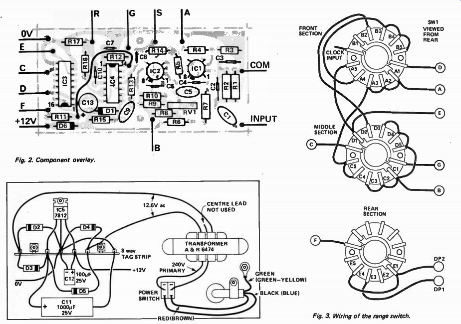
Fig. 2. Component overlay.
Fig. 3. Wiring of the range switch.

Fig. 4. How the power supply is mounted on the back panel and interconnected.
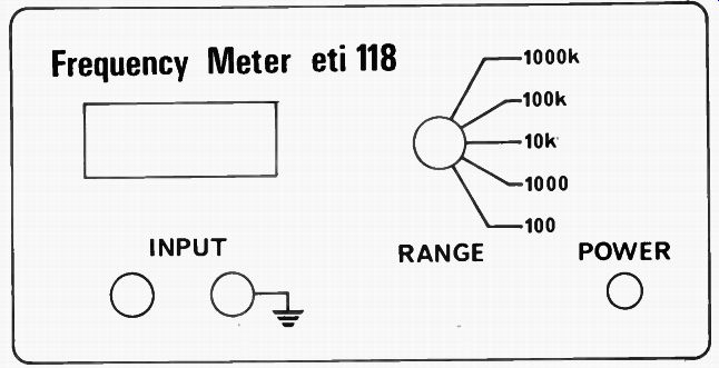
Fig. 5. Front panel of the frequency meter.
Initially the maximum frequency of operation was limited to 200 kHz due to the slow, negative slew-rate of the IC. Looking at the internal circuit of the IC it was decided to increase the bias current in the second stage by adding a resistor between the positive supply and pin 8. This allows the frequency response to be extended to beyond one megahertz. A small compensating capacitor was found to be necessary to eliminate the effects of a small amount of coupling from the 10 Hz oscillator. The resistor to pin 8 also alters the offset voltage but this does not affect the operation of this circuit.
Another problem that occurred was in the strobe and reset pulse network.
Using an 0.1 second timebase the display changes too rapidly for ease of reading. Therefore IC4/4, which is connected as a 350 millisecond monostable, is used to eliminate three out of every four strobe pulses thus making the display more readable.
However it was discovered that, when using this delay, the timebase changed frequency by about four parts in 10000. Since the power supply to the control circuitry was isolated from the display module, the circuitry is mainly CMOS, and the oscillator rejects supply rail change, none of these factors could be suspected as a cause of the trouble. The problem was due to the fact that IC4/4 works in the linear mode and can draw 10 to 20 mA. This modulates the power supply by up to 20 millivolts. The cure is to power IC4 directly from the 12 volts.
This explains the use of the link of the board.
Some coupling between the display board oscillator and the input stage occurred and was cured by adding an aluminum shield between the two boards.
To obtain all five ranges with only two divide- by-ten sections necessitates a more complex switch. This was considered to be justifiable as the alternative was to use a switch with one less wafer but add one more 14518 IC.
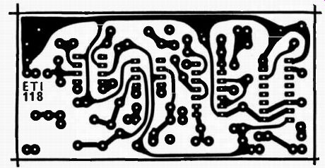
Fig. 6. Printed circuit board for the counter. Full size 90 x 45 mm.
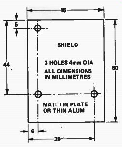
Fig. 7. Drilling details of the shield plate.
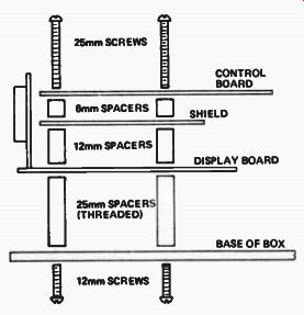
Fig. 8. Assembly of the counter display boards.
----------------
TABLE 1
Frequency with RV1 at minimum
50 Hz input Value of R9 to allow RV1 to calibrate
48.1 - 50 49.8 - 51.8 51.3 - 53.4 52.7 - 55.0 54.7 - 57.1 56.7 - 59.3 58.8 - 61.7 15 Meg 8.2 Meg 5.6 Meg 3.9 Meg 3.0 Meg 2.4 Meg
---------------
CONSTRUCTION
The display module should be constructed as described on pages 20 and 21. The value of resistors R5 to R11 should be 560 ohms for operation of the 12 volt supply.
The control board should be assembled with the aid of the component overlay Fig. 2. Use printed circuit board pins for all outputs and for R9 as an aid to later assembly.
Make sure that the link between + 12 volts and pin 14 of IC4 is installed.
Wire switch SW1, in accordance with Fig. 3, and leave the leads long enough to reach the printed circuit board.
Assemble the power supply onto the tag strip and the back panel of the box as detailed in Fig. 4. There is no need to insulate the tag of the regulator from the rear panel as it is the common terminal which should be earthed. The rear panel itself is earthed via the mains cable.
The front panel has to be cut and drilled as shown in Fig. 5. It can be either silk screened with the required range markings etc, or a Scotchcal panel can be used as in our prototype.
Scotchcal panels for this project can be obtained for $3.00 (plus SAE) directly from Electronics Today.
A piece of polarized or red plastic can be used to protect the displays. If the A&R box, as specified, is used mounting holes will have to be drilled in the base of the box. These can be marked by temporarily installing the front panel, by fitting the three 25 mm spacers to the control module (the left front mounting hole on the module is not used) and sitting the control module in position. It will be found that the right front spacer interferes with a rib in the base of the box. Cut this rib away with a chisel or similar tool such that the spacer can sit flush with the base. Mark the hole positions, remove the module and drill the holes.
Fit the rear panel in to the box and then mount the input terminals to the front panel (the rear of the screws of the terminals may have to be shortened to clear the display module mounting spacers). The rotary and toggle switches should also now be mounted to the front panel. Connect a short length of coaxial cable to the input terminals ( about 150 mm) for later connection to the control board.
Connect leads to the positive volt, zero volt, strobe, reset and input clock inputs on the display module and assemble the display board, shield and control board as shown in Fig. 8.Make sure that the spacers do not touch the copper tracks on any of the boards, (except for the front spacer on the control board). If any of the spacers are too close to the tracks add a piece of insulation material under the spacer. The whole assembly can now be mounted in to the box.
On the display module the power rails are taken direct to the power supply whilst the ' reset' and 'strobe' go to the control board and the 'control' to the rotary switch. On the control board the power rails also go direct to the power supply whilst all other leads, with the exception of the coaxial cable, go to the rotary switch.
Finally connect the power switch and insulate it with plastic tape to prevent accidental personal contact.
CALIBRATION
Apply about 6 volts ac at 50 Hz, from the secondary of a power transformer to the input of the counter. Select the 100 Hz range and set the trimpot, RV1, to its minimum resistance position. Wait for the reading to settle ( there is about ten seconds between readings) and using this reading look up the corresponding value of R9 from Table 1. Install this resistor and again check the reading, it should now be just under 50 Hz. The trimpot RV1 can now be adjusted to give a reading of exactly 50 Hz. If a more accurate frequency source than the mains is available it can be used instead of the 50 Hz for final calibration. Due to the effect of soldering upon the value of resistors final calibration should be left until several hours after R9 is soldered into position so that the resistor ma i ; stabilize.
------------